US7567311B2 - Liquid crystal display device - Google Patents
Liquid crystal display device Download PDFInfo
- Publication number
- US7567311B2 US7567311B2 US12/007,691 US769108A US7567311B2 US 7567311 B2 US7567311 B2 US 7567311B2 US 769108 A US769108 A US 769108A US 7567311 B2 US7567311 B2 US 7567311B2
- Authority
- US
- United States
- Prior art keywords
- insulating layer
- layer
- semiconductor layer
- bus line
- data bus
- Prior art date
- Legal status (The legal status is an assumption and is not a legal conclusion. Google has not performed a legal analysis and makes no representation as to the accuracy of the status listed.)
- Active, expires
Links
Images


Classifications
-
- G—PHYSICS
- G02—OPTICS
- G02F—OPTICAL DEVICES OR ARRANGEMENTS FOR THE CONTROL OF LIGHT BY MODIFICATION OF THE OPTICAL PROPERTIES OF THE MEDIA OF THE ELEMENTS INVOLVED THEREIN; NON-LINEAR OPTICS; FREQUENCY-CHANGING OF LIGHT; OPTICAL LOGIC ELEMENTS; OPTICAL ANALOGUE/DIGITAL CONVERTERS
- G02F1/00—Devices or arrangements for the control of the intensity, colour, phase, polarisation or direction of light arriving from an independent light source, e.g. switching, gating or modulating; Non-linear optics
- G02F1/01—Devices or arrangements for the control of the intensity, colour, phase, polarisation or direction of light arriving from an independent light source, e.g. switching, gating or modulating; Non-linear optics for the control of the intensity, phase, polarisation or colour
- G02F1/13—Devices or arrangements for the control of the intensity, colour, phase, polarisation or direction of light arriving from an independent light source, e.g. switching, gating or modulating; Non-linear optics for the control of the intensity, phase, polarisation or colour based on liquid crystals, e.g. single liquid crystal display cells
- G02F1/133—Constructional arrangements; Operation of liquid crystal cells; Circuit arrangements
- G02F1/136—Liquid crystal cells structurally associated with a semi-conducting layer or substrate, e.g. cells forming part of an integrated circuit
- G02F1/1362—Active matrix addressed cells
- G02F1/136227—Through-hole connection of the pixel electrode to the active element through an insulation layer
Definitions
- the present invention relates to a display device and a method of fabricating a display device, and more particularly to a liquid crystal display (LCD) device and a method of fabricating an LCD device.
- LCD liquid crystal display
- LCD devices are commonly used for their superior color reproduction.
- an LCD device includes two substrates facing each other, wherein electrodes are formed on opposing facing surfaces of the two substrates, and a liquid crystal material is injected into a space defined between the two substrates.
- the LCD device displays images by applying a voltage between the electrodes on both the substrates to induce an electric field to the liquid crystal material, thereby changing alignment orientation of liquid crystal molecules of the liquid crystal material to vary light transmittance through the liquid crystal material.
- the first of the two substrates of the LCD device includes a matrix array of thin film transistors (TFTs), wherein an active layer of each of the TFTs is generally formed of amorphous silicon (a-Si:H). This is because the amorphous silicon can be formed on large-sized glass substrates at relatively low temperatures.
- TFTs thin film transistors
- LCD devices employ TFTs using polycrystalline silicon (polysilicon) as an active layer. Since the polysilicon has an electric field effect mobility, which is 100 to 200 times greater than that of amorphous silicon, the LCD employing polysilicon TFTs has fast response speeds and stability against extreme temperature ranges and light. In addition, since driving circuits can be formed on the substrate, it is possible to reduce fabrication costs of the LCD device.
- polysilicon polycrystalline silicon
- the polysilicon can be formed using various different methods, such as laser annealing, metal induced crystallization (MIC), and solid phase crystallization (SPC).
- laser annealing method a laser beam is irradiated onto an amorphous silicon layer using an excimer laser while heating the substrate to a temperature of 250° C., thereby growing a polysilicon layer.
- MIC method metal induced crystallization
- SPC method solid phase crystallization
- a metal film is deposited onto an amorphous silicon layer and a polysilicon layer is grown using the metal film as a seed for nucleation.
- SPC method an amorphous silicon layer is annealed at high temperature for an extended period of time.
- another method includes depositing a polysilicon layer directly onto a substrate.
- SLS sequential lateral solidification
- FIGS. 1A to 1E are schematic cross sectional views of a method of fabricating a Buried Bus Coplanar (BBC) polysilicon TFT according to the related art.
- BBC Buried Bus Coplanar
- an interlayer insulating layer 135 formed of an inorganic material, such as SiNx or SiOx, or an organic insulator is formed on the data bus line 130 and the substrate 110 . Then, a semiconductor layer 180 of polysilicon is formed having a predetermined pattern on the interlayer insulating layer 135 .
- a gate insulating layer 125 of inorganic material is formed on the semiconductor 180 and the substrate 110 .
- a gate electrode 120 and a gate bus line are formed on the gate insulating layer 125 by depositing a second metal film on the gate insulating layer 125 and patterning the second metal film.
- P + impurity ions are implanted into the semiconductor layer 180 using the gate electrode 120 as a mask.
- the implanted impurity ions are activated by a laser beam, thereby forming a source region and a drain region at predetermined portions of the semiconductor layer 180 .
- a passivation layer 165 of inorganic or organic material is formed on the gate electrode 120 and the gate insulating layer 125 . Then, a first contact hole exposing a part of the data bus line 130 , and second and third contact holes 109 b and 109 c exposing a part of the semiconductor layer 180 are formed in the passivation layer 165 .
- an indium tin oxide (ITO) layer is deposited on the passivation layer 165 including the first, second, and third contact holes 109 a , 109 b , and 109 c , and is then patterned, thereby forming a pixel electrode 140 electrically in contact with the impurity-doped semiconductor layer 180 .
- a source electrode 140 a is formed by electrically connecting the data bus line 130 with the impurity-doped semiconductor layer 180 through the first contact hole 109 a and the second contact hole 109 b .
- a drain electrode is formed together with the pixel electrode 140 by the ITO layer filled within the third contact hole 109 c.
- first, second, and third contact holes 109 a , 109 b , and 109 c are formed, an exposed portion of the data bus line 130 and exposed portions of the semiconductor layer 180 are oxidized.
- contact resistance between the ITO layer filled within the first contact hole 109 a and the exposed data bus line 130 increases.
- contact resistance between the ITO layer filled within the second and third contact holes 109 b and 109 c and the exposed semiconductor layer 180 increases. Accordingly, the increased contact resistances causes signal delays, thereby reducing image quality and reliability of the LCD device.
- the data bus line 130 including the source electrode is positioned below the semiconductor layer 180 .
- the interlayer insulating layer 135 is deposited at a thickness of 3,000 ⁇ , and the semiconductor layer 180 is formed.
- the semiconductor layer 180 formed of amorphous silicon has different thicknesses between a stepped portion and a plane portion. Due to the different thicknesses, the polysilicon layer, which is crystallized by laser annealing of the amorphous silicon, becomes very thin at a predetermined portion so that non-uniform crystalline property of the active region and ablation phenomenon occur.
- the first contact hole 109 a is formed by etching the passivation layer 165 , the gate insulating layer 125 , and the interlayer insulating layer 135 to expose a portion of the data bus line 130 .
- the second and third contact holes 109 b and 109 c are formed by etching the passivation layer 165 and the gate insulating layer 125 to expose portions of the semiconductor layer 180 .
- the impurity-doped semiconductor layer 180 is subject to etching damage, thereby deteriorating operational characteristics of the LCD device due to partial loss of semiconductor layer 180 .
- the present invention is directed to an LCD device and method of fabricating an LCD device that substantially obviates one or more problems due to limitations and disadvantages of the related art.
- It is an object of the present invention is to provide an LCD device that prevents an increase of contact resistance and signal delay.
- Another object of the present invention is to provide a method of fabricating an LCD device that prevents an increase of contact resistance and signal delay.
- Another object of the present invention is to provide an LCD device having a reduced height difference within a stepped portion of a semiconductor layer.
- Another object of the present invention is to provide a method of fabricating an LCD device that can minimize loss of a semiconductor layer.
- a method of fabricating a liquid crystal display device includes forming a data bus line, an interlayer insulating layer, a semiconductor layer, a gate insulating layer, and a gate electrode on a first surface of a substrate, forming a passivation layer on the substrate, forming a photoresist film on the passivation layer, forming a photoresist pattern from the photoresist film to expose portions of the passivation layer, etching the passivation layer to form a plurality of first contact holes exposing portions of the semiconductor layer and etching the passivation layer and the semiconductor layer to form a second contact hole exposing a portion of the data bus line, the photoresist pattern having a plurality of undercut regions corresponding to each of the first and second contact holes, depositing a first portion of a metal film on the photoresist pattern and a plurality of second portions of the metal film within each of the first
- a method of fabricating a liquid crystal display device includes forming a data bus line on a substrate, forming a preliminary interlayer insulating layer having a first thickness on the substrate including the data bus line, forming an interlayer insulating layer by etching the preliminary interlayer insulating layer to a second thickness less than the first thickness, the interlayer insulating layer having a planarized surface, sequentially forming a semiconductor layer, a gate insulating layer, and a gate electrode on the interlayer insulating layer, forming a passivation layer on the substrate, forming a plurality of contact holes exposing portions of the data bus line and the semiconductor layer by etching portions of the passivation layer, and forming a pixel electrode on the passivation layer.
- a liquid crystal display device in another aspect, includes a substrate, a data bus line formed on the substrate, an interlayer insulating layer formed on the data bus line and the substrate, a semiconductor layer formed on the interlayer insulating layer, a gate insulating layer formed on the semiconductor layer, a gate electrode formed on the gate insulating layer above the semiconductor layer, a passivation layer formed on the gate electrode and the gate insulating layer, the passivation layer having a plurality of contact holes exposing portions of the data bus line and the semiconductor layer, a metal film formed on the data bus line and the semiconductor layer within the contact holes, and a pixel electrode formed on the passivation layer and electrically connected to the metal film within one of the contact holes on the semiconductor layer.
- FIGS. 1A to 1E are schematic cross sectional views of a method of fabricating a Buried Bus Coplanar (BBC) polysilicon TFT according to the related art;
- BBC Buried Bus Coplanar
- FIG. 2 is a schematic plan view of an exemplary array substrate of an LCD device according to the present invention.
- FIGS. 3A to 3H are cross sectional views along I-I′ of FIG. 2 of an exemplary method of fabricating an array substrate of an LCD device according to the present invention.
- FIG. 2 is a schematic plan view of an exemplary array substrate of an LCD device according to the present invention.
- an LCD device 200 may include a pixel electrode 240 formed at a crossing region of a gate bus line 221 and a data bus line 230 .
- the pixel electrode 240 may electrically contact a TFT having a gate electrode 220 , a source electrode 240 a , a drain electrode 230 a , and a semiconductor layer 280 .
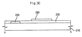
- FIGS. 3A to 3H are cross sectional views along I-I′ of FIG. 2 of an exemplary method of fabricating an array substrate of an LCD device according to the present invention.
- a pattern of the data bus line 230 may be formed of a first metal film on a substrate 210 .
- an interlayer insulating layer 235 may be formed of an inorganic or organic insulating material to cover the data bus line 230 .
- the interlayer insulating layer 235 may be deposited onto the substrate 210 at a thickness greater than a thickness of the data bus line 230 , such as about 4000 ⁇ to about 8000 ⁇ .
- the interlayer insulating layer 235 may be etched using an etching process to reduce the thickness of the interlayer insulating layer 235 , and to planarize the interlayer insulating layer 235 .
- the etching process may be performed using dry or wet etching.
- the interlayer insulating layer 235 may be planarized using a chemical and mechanical polishing (CMP) process. Accordingly, the interlayer insulating layer 235 is planarized until the interlayer insulating layer 235 has a height similar to a height with a peripheral region of the LCD device.
- CMP chemical and mechanical polishing
- the interlayer insulating layer 235 may be formed of a dual layer using Spin-On-Glass (SOG) including SiNx, SiOx, or PE-oxide based materials, and etched.
- SOG Spin-On-Glass
- SiNx or PE-oxide based material may be deposited onto the substrate 210 to a first thickness, and then SOG may be deposited to form the dual layer of SiNx or PE-oxide based material and SOG.
- the dual layer may be annealed to remove carbon (C) components to enhance density, and may be etched for planarization.
- SiNx or PE-oxide based materials may be again deposited or only the SOG may be re-deposited.
- the semiconductor layer 280 may be formed of polysilicon on the planarized interlayer insulating layer 235 to have a patterned shape.
- a gate insulating layer 225 may be formed of an inorganic insulating layer onto the substrate 210 having the semiconductor layer 280 . Then, a second metal film may be deposited onto the gate insulating layer 225 , and patterned to form the gate electrode 220 and the gate bus line (not shown). Next, P + ions may be doped into the semiconductor layer 280 using the patterned second metal film as a mask. Then, a laser beam may be irradiated onto the doped semiconductor layer 280 to form source/drain regions. Accordingly, irradiation of the laser beam may anneal damage to the semiconductor layer 280 caused during the doping of the P + ions, and the P + ions may be activated.
- a passivation layer 265 formed of an inorganic or organic insulating material and a photoresist film 275 may be formed to cover the gate electrode 220 and the gate insulating layer 225 .
- the passivation layer 265 may prevent the TFT from being damaged or degraded due to subsequent rubbing processing of LCD cells of the LCD device.
- the passivation layer 265 may prevent formation of scratches and moisture permeation during subsequent processing of the LCD device.
- the passivation layer 265 may be formed of silicon nitride or BenzoCyclo-Butene (BCB), which is an organic insulating material.
- the photoresist film 275 may be exposed to UV light using a mask having a predetermined pattern.
- UV light may be used to subsequently form contact holes.
- the photoresist film 275 may be exposed and developed using a developer, thereby removing the exposed portions of the photoresist film 275 . After that, the resultant structure may be etched.
- exposed portions of the passivation layer 265 , the gate insulating layer 225 , and the interlayer insulating layer 235 may be wet-etched. Accordingly, a first contact hole 209 a may be formed to expose a portion of the data bus line 230 , and second and third contact holes 209 b and 209 c may be formed to expose portions of the doped semiconductor layer 280 .
- the etched portions of the photoresist film 275 may be undercut due to relational wet-etching characteristics of the passivation layer 265 and the photoresist film 275 . The undercut may prevent a subsequently-formed metal film from being deposited onto the undercut portion of the photoresist film 275 when the metal film to be lifted off is deposited onto the resultant structure of the substrate 210 .
- a metal film 268 a may be deposited onto the photoresist pattern 275 having the first, second, and third contact holes 209 a , 209 b , and 209 c .
- the metal film 268 a may be deposited using a sputtering method.
- the metal film 268 a may be formed of an oxidation-resistant metal, such as chromium (Cr), molybdenum (Mo), tungsten (W), titanium (Ti)-based material, or an aluminum alloy.
- the photoresist film 275 may be removed using a stripper, wherein the photoresist pattern 275 may be removed and portions of the metal film 268 a deposited on the photoresist pattern 275 may be removed using a lift-off process.
- the lift-off process using the photoresist film 275 is advantageous in that the stripper easily permeates into the photoresist film 275 through the undercut portions to melt the photoresist film 275 , thereby providing a clean, clear pattern.
- a thin metal film 268 b may be deposited into the first, second, and third contact holes 209 a , 209 b , and 209 c (in FIG. 3H ). Accordingly, the thin metal film 268 b may partially remain to contact the data bus line 230 and the semiconductor layer 280 .
- the thin metal film 268 b may have oxidation-resistance, thereby preventing surface oxidation on the data bus line 230 and the semiconductor layer 280 . Thus, increased contact resistance between a subsequently-formed pixel electrode and the semiconductor layer 280 may be prevented.
- a transparent conductive material may be formed within the first, second, and third contact holes 209 a , 209 b , and 209 c . Then, the transparent conductive material may be patterned to form a pixel electrode 240 that contacts the doped semiconductor layer 280 .
- ITO indium-tin-oxide
- IZO indium-zinc-oxide
- ITZO indium-tin-zinc-oxide
- a source electrode 240 a may be formed to connect the data bus line 230 with the doped semiconductor layer 280 through the first contact hole 209 a and the second contact hole 209 b .
- the drain electrode may be formed to contact the pixel electrode 240 through the third contact hole 209 c.
- a lift-off process may be used to deposit the oxidation-resistant metal film within contact holes without using a separate mask, thereby preventing surface oxidation. Accordingly, since exposed surfaces of the data bus line and the semiconductor layer may not be oxidized, contact resistance may not increase and signal delay may be prevented, thereby minimizing product failure and improving productivity.
- a step portion that is generated when an insulating layer is formed may be planarized, thereby preventing loss of a semiconductor layer due to formation of contact holes and preventing disconnection during crystallization of the semiconductor layer, thereby improving product reliability.
Abstract
Description
Claims (5)
Priority Applications (1)
| Application Number | Priority Date | Filing Date | Title |
|---|---|---|---|
| US12/007,691 US7567311B2 (en) | 2003-06-27 | 2008-01-14 | Liquid crystal display device |
Applications Claiming Priority (4)
| Application Number | Priority Date | Filing Date | Title |
|---|---|---|---|
| KR1020030042845A KR100558985B1 (en) | 2003-06-27 | 2003-06-27 | A fabrication method of a array substrate for LCD |
| KR10-2003-0042845 | 2003-06-27 | ||
| US10/863,235 US7342631B2 (en) | 2003-06-27 | 2004-06-09 | Liquid crystal display device and method of fabricating the same |
| US12/007,691 US7567311B2 (en) | 2003-06-27 | 2008-01-14 | Liquid crystal display device |
Related Parent Applications (1)
| Application Number | Title | Priority Date | Filing Date |
|---|---|---|---|
| US10/863,235 Division US7342631B2 (en) | 2003-06-27 | 2004-06-09 | Liquid crystal display device and method of fabricating the same |
Publications (2)
| Publication Number | Publication Date |
|---|---|
| US20080136987A1 US20080136987A1 (en) | 2008-06-12 |
| US7567311B2 true US7567311B2 (en) | 2009-07-28 |
Family
ID=33536352
Family Applications (2)
| Application Number | Title | Priority Date | Filing Date |
|---|---|---|---|
| US10/863,235 Active 2024-11-05 US7342631B2 (en) | 2003-06-27 | 2004-06-09 | Liquid crystal display device and method of fabricating the same |
| US12/007,691 Active 2024-10-11 US7567311B2 (en) | 2003-06-27 | 2008-01-14 | Liquid crystal display device |
Family Applications Before (1)
| Application Number | Title | Priority Date | Filing Date |
|---|---|---|---|
| US10/863,235 Active 2024-11-05 US7342631B2 (en) | 2003-06-27 | 2004-06-09 | Liquid crystal display device and method of fabricating the same |
Country Status (2)
| Country | Link |
|---|---|
| US (2) | US7342631B2 (en) |
| KR (1) | KR100558985B1 (en) |
Families Citing this family (13)
| Publication number | Priority date | Publication date | Assignee | Title |
|---|---|---|---|---|
| US7316942B2 (en) * | 2005-02-14 | 2008-01-08 | Honeywell International, Inc. | Flexible active matrix display backplane and method |
| JP4805587B2 (en) * | 2005-02-24 | 2011-11-02 | エーユー オプトロニクス コーポレイション | Liquid crystal display device and manufacturing method thereof |
| US7952099B2 (en) * | 2006-04-21 | 2011-05-31 | Beijing Boe Optoelectronics Technology Co., Ltd. | Thin film transistor liquid crystal display array substrate |
| CN100449392C (en) * | 2006-08-04 | 2009-01-07 | 北京京东方光电科技有限公司 | Thin-film transistor LCD pixel structure and manufacturing method therefor |
| CN100452412C (en) * | 2007-05-31 | 2009-01-14 | 友达光电股份有限公司 | Pixel structure and manufacture method and photoelectronic device with the pixel structure and manufacture method |
| JP2009058717A (en) * | 2007-08-31 | 2009-03-19 | Seiko Epson Corp | Electro-optical device, its manufacturing method, and electronic equipment |
| KR101298612B1 (en) * | 2010-10-12 | 2013-08-26 | 엘지디스플레이 주식회사 | Array substrate for in plane switching mode liquid crystal display device and method for fabricating the same |
| CN104157613B (en) * | 2014-07-31 | 2017-03-08 | 京东方科技集团股份有限公司 | A kind of preparation method of array base palte |
| KR102395900B1 (en) | 2015-06-26 | 2022-05-09 | 삼성디스플레이 주식회사 | Display apparatus and manuacturing method thereof |
| CN105514125B (en) * | 2016-02-02 | 2019-07-12 | 京东方科技集团股份有限公司 | A kind of array substrate, preparation method and display panel |
| WO2019084077A1 (en) * | 2017-10-27 | 2019-05-02 | Corning Incorporated | Through glass via fabrication using a protective material |
| CN113497090B (en) * | 2020-03-20 | 2023-09-22 | 合肥鑫晟光电科技有限公司 | Display substrate, manufacturing method thereof and display panel |
| CN113702446B (en) * | 2021-09-03 | 2023-11-03 | 松山湖材料实验室 | Micro-resistance testing method for ceramic substrate through hole |
Citations (5)
| Publication number | Priority date | Publication date | Assignee | Title |
|---|---|---|---|---|
| US5642212A (en) * | 1993-02-03 | 1997-06-24 | Sharp Kabushiki Kaisha | Display apparatus having a two-terminal device including a zinc sulfide layer and method for producing the same |
| KR20010001346A (en) | 1999-06-03 | 2001-01-05 | 구본준 | LCD device and the same method |
| US20020018152A1 (en) * | 2000-06-02 | 2002-02-14 | Tetsuya Nagata | Liquid crystal display device |
| KR20020057032A (en) | 2000-12-30 | 2002-07-11 | 주식회사 현대 디스플레이 테크놀로지 | Method for manufacturing thin film transistor liquid crystal display device |
| US6894754B2 (en) * | 2002-03-28 | 2005-05-17 | Sharp Kabushiki Kaisha | Substrate with a flattening film, display substrate, and method of manufacturing the substrates |
-
2003
- 2003-06-27 KR KR1020030042845A patent/KR100558985B1/en not_active IP Right Cessation
-
2004
- 2004-06-09 US US10/863,235 patent/US7342631B2/en active Active
-
2008
- 2008-01-14 US US12/007,691 patent/US7567311B2/en active Active
Patent Citations (5)
| Publication number | Priority date | Publication date | Assignee | Title |
|---|---|---|---|---|
| US5642212A (en) * | 1993-02-03 | 1997-06-24 | Sharp Kabushiki Kaisha | Display apparatus having a two-terminal device including a zinc sulfide layer and method for producing the same |
| KR20010001346A (en) | 1999-06-03 | 2001-01-05 | 구본준 | LCD device and the same method |
| US20020018152A1 (en) * | 2000-06-02 | 2002-02-14 | Tetsuya Nagata | Liquid crystal display device |
| KR20020057032A (en) | 2000-12-30 | 2002-07-11 | 주식회사 현대 디스플레이 테크놀로지 | Method for manufacturing thin film transistor liquid crystal display device |
| US6894754B2 (en) * | 2002-03-28 | 2005-05-17 | Sharp Kabushiki Kaisha | Substrate with a flattening film, display substrate, and method of manufacturing the substrates |
Non-Patent Citations (1)
| Title |
|---|
| Communication from Korean Patent Office. |
Also Published As
| Publication number | Publication date |
|---|---|
| KR20050001263A (en) | 2005-01-06 |
| US7342631B2 (en) | 2008-03-11 |
| KR100558985B1 (en) | 2006-03-10 |
| US20040263742A1 (en) | 2004-12-30 |
| US20080136987A1 (en) | 2008-06-12 |
Similar Documents
| Publication | Publication Date | Title |
|---|---|---|
| US7567311B2 (en) | Liquid crystal display device | |
| US7999267B2 (en) | Liquid crystal display device | |
| US8158469B2 (en) | Method of fabricating array substrate | |
| US7666695B2 (en) | Array substrates of liquid crystal display and fabrication method thereof | |
| US8049830B2 (en) | Liquid crystal display device and fabrication method thereof | |
| US7396765B2 (en) | Method of fabricating a liquid crystal display device | |
| US6395586B1 (en) | Method for fabricating high aperture ratio TFT's and devices formed | |
| US6627471B2 (en) | Method of manufacturing an array substrate having drive integrated circuits | |
| US5953085A (en) | Liquid crystal display device having a storage capacitor | |
| US7414691B2 (en) | Liquid crystal display device with prevention of defective disconnection of drain/pixel electrodes by forming two conductive layers on top of entire pixel electrode and then removing a portion of both therefrom | |
| US7479415B2 (en) | Fabrication method of polycrystalline silicon liquid crystal display device | |
| KR20050029512A (en) | Poly silicon thin film transistor and the fabrication method thereof | |
| JP4312179B2 (en) | Liquid crystal display element and manufacturing method thereof | |
| KR101051004B1 (en) | An array substrate for LCD with type TFT and method of fabrication thereof | |
| US8018545B2 (en) | Method of fabricating a liquid crystal display device | |
| KR20050070240A (en) | Poly silicon thin film transistor and the fabrication method thereof | |
| KR101338104B1 (en) | Method of fabricating tft array substrate | |
| KR20020032196A (en) | Polysilicon-thin film transistor device and method of fabricating the same | |
| US7701524B2 (en) | LCD device comprising the drain electrode connected to an upper and a side portion of the pixel electrode and fabrication method thereof | |
| KR100545028B1 (en) | Thin film patterning method and manufacturing method of thin film transistor array substrate | |
| KR100242946B1 (en) | Thin-flim transistor and manufacturing method thereof | |
| JPH11345975A (en) | Thin film transistor and its manufacture | |
| JP2003215634A (en) | Thin film transistor liquid crystal display device | |
| KR20010082829A (en) | Method for Fabricating Thin Film Transistor And Method for Fabricating Liquid Crystal Display Device Using the same | |
| KR20020055990A (en) | Method for Fabricating Thin Film Transistor of Poly Silicon Type |
Legal Events
| Date | Code | Title | Description |
|---|---|---|---|
| AS | Assignment |
Owner name: LG.PHILIPS LCD CO., LTD., KOREA, REPUBLIC OF Free format text: ASSIGNMENT OF ASSIGNORS INTEREST;ASSIGNOR:KIM, SANG HYUN;REEL/FRAME:020404/0937 Effective date: 20040604 |
|
| FEPP | Fee payment procedure |
Free format text: PAYOR NUMBER ASSIGNED (ORIGINAL EVENT CODE: ASPN); ENTITY STATUS OF PATENT OWNER: LARGE ENTITY |
|
| AS | Assignment |
Owner name: LG DISPLAY CO., LTD., KOREA, REPUBLIC OF Free format text: CHANGE OF NAME;ASSIGNOR:LG.PHILIPS LCD CO., LTD.;REEL/FRAME:021952/0300 Effective date: 20080304 Owner name: LG DISPLAY CO., LTD.,KOREA, REPUBLIC OF Free format text: CHANGE OF NAME;ASSIGNOR:LG.PHILIPS LCD CO., LTD.;REEL/FRAME:021952/0300 Effective date: 20080304 |
|
| STCF | Information on status: patent grant |
Free format text: PATENTED CASE |
|
| FEPP | Fee payment procedure |
Free format text: PAYOR NUMBER ASSIGNED (ORIGINAL EVENT CODE: ASPN); ENTITY STATUS OF PATENT OWNER: LARGE ENTITY |
|
| FPAY | Fee payment |
Year of fee payment: 4 |
|
| FPAY | Fee payment |
Year of fee payment: 8 |
|
| MAFP | Maintenance fee payment |
Free format text: PAYMENT OF MAINTENANCE FEE, 12TH YEAR, LARGE ENTITY (ORIGINAL EVENT CODE: M1553); ENTITY STATUS OF PATENT OWNER: LARGE ENTITY Year of fee payment: 12 |