US7550760B2 - Polyacenes and electronic devices generated therefrom - Google Patents
Polyacenes and electronic devices generated therefrom Download PDFInfo
- Publication number
- US7550760B2 US7550760B2 US11/399,216 US39921606A US7550760B2 US 7550760 B2 US7550760 B2 US 7550760B2 US 39921606 A US39921606 A US 39921606A US 7550760 B2 US7550760 B2 US 7550760B2
- Authority
- US
- United States
- Prior art keywords
- silyl
- tri
- accordance
- zero
- hydrocarbon
- Prior art date
- Legal status (The legal status is an assumption and is not a legal conclusion. Google has not performed a legal analysis and makes no representation as to the accuracy of the status listed.)
- Active, expires
Links
- 0 CC(C)c(ccc1c2)cc1cc1c2c(C#C*)c(cc(C(C)C)cc2)c2c1C#C* Chemical compound CC(C)c(ccc1c2)cc1cc1c2c(C#C*)c(cc(C(C)C)cc2)c2c1C#C* 0.000 description 25
Images


Classifications
-
- C—CHEMISTRY; METALLURGY
- C08—ORGANIC MACROMOLECULAR COMPOUNDS; THEIR PREPARATION OR CHEMICAL WORKING-UP; COMPOSITIONS BASED THEREON
- C08G—MACROMOLECULAR COMPOUNDS OBTAINED OTHERWISE THAN BY REACTIONS ONLY INVOLVING UNSATURATED CARBON-TO-CARBON BONDS
- C08G61/00—Macromolecular compounds obtained by reactions forming a carbon-to-carbon link in the main chain of the macromolecule
- C08G61/02—Macromolecular compounds containing only carbon atoms in the main chain of the macromolecule, e.g. polyxylylenes
-
- H—ELECTRICITY
- H10—SEMICONDUCTOR DEVICES; ELECTRIC SOLID-STATE DEVICES NOT OTHERWISE PROVIDED FOR
- H10K—ORGANIC ELECTRIC SOLID-STATE DEVICES
- H10K85/00—Organic materials used in the body or electrodes of devices covered by this subclass
- H10K85/10—Organic polymers or oligomers
- H10K85/111—Organic polymers or oligomers comprising aromatic, heteroaromatic, or aryl chains, e.g. polyaniline, polyphenylene or polyphenylene vinylene
- H10K85/114—Poly-phenylenevinylene; Derivatives thereof
-
- H—ELECTRICITY
- H10—SEMICONDUCTOR DEVICES; ELECTRIC SOLID-STATE DEVICES NOT OTHERWISE PROVIDED FOR
- H10K—ORGANIC ELECTRIC SOLID-STATE DEVICES
- H10K10/00—Organic devices specially adapted for rectifying, amplifying, oscillating or switching; Organic capacitors or resistors having potential barriers
- H10K10/40—Organic transistors
- H10K10/46—Field-effect transistors, e.g. organic thin-film transistors [OTFT]
- H10K10/462—Insulated gate field-effect transistors [IGFETs]
- H10K10/464—Lateral top-gate IGFETs comprising only a single gate
-
- H—ELECTRICITY
- H10—SEMICONDUCTOR DEVICES; ELECTRIC SOLID-STATE DEVICES NOT OTHERWISE PROVIDED FOR
- H10K—ORGANIC ELECTRIC SOLID-STATE DEVICES
- H10K10/00—Organic devices specially adapted for rectifying, amplifying, oscillating or switching; Organic capacitors or resistors having potential barriers
- H10K10/40—Organic transistors
- H10K10/46—Field-effect transistors, e.g. organic thin-film transistors [OTFT]
- H10K10/462—Insulated gate field-effect transistors [IGFETs]
- H10K10/466—Lateral bottom-gate IGFETs comprising only a single gate
Definitions
- the present disclosure is generally directed to polyacenes and uses thereof. More specifically, the present disclosure in embodiments is directed to a class of polyacenes selected as solution processable and substantially stable channel semiconductors in organic electronic devices, such as thin film transistors.
- TFT thin film transistors
- flexible TFTs enable the design of electronic devices with structural flexibility and mechanical durability characteristics.
- the use of plastic substrates together with the polyacene components can transform the traditionally rigid silicon TFT into a mechanically more durable and structurally flexible TFT design.
- large area devices such as large-area image sensors, electronic paper and other display media.
- polyacene TFTs for integrated circuit logic elements for low end microelectronics such as smart cards, radio frequency identification (RFID) tags, and memory/storage devices, may enhance their mechanical durability, and thus their useful life span.
- RFID radio frequency identification
- Acenes such as pentacene and heteroacenes, are known to possess acceptable field effect mobility, however, these materials are rapidly oxidized by, for example, atmospheric oxygen under light, and such compounds are not considered processable at ambient conditions. Furthermore, when selected for TFTs acenes tend to have poor thin film formation characteristics and are substantially insoluble thus they are essentially nonsolution processable; accordingly, such compounds have been primarily processed by vacuum deposition methods that result in high production costs, eliminated or minimized with the TFTs generated with the functionalized heterocenes illustrated herein.
- organic semiconductor materials include organic small molecules, such as pentacene, see for example D. J. Gundlach et al., “Pentacene organic thin film transistors—molecular ordering and mobility”, IEEE Electron Device Lett., Vol. 18, p. 87 (1997); oligomers, such as sexithiophenes or their variants, see for example reference F. Garnier et al., “Molecular engineering of organic semiconductors: Design of self-assembly properties in conjugated thiophene oligomers”, J. Amer. Chem. Soc., Vol. 115, p.
- organic material based TFTs generally provide lower performance characteristics than their conventional silicon counterparts, such as silicon crystal or polysilicon TFTs, they are nonetheless sufficiently useful for applications in areas where high mobility is not required. These include large area devices, such as image sensors, active matrix liquid crystal displays and low end microelectronics, such as smart cards and RFID tags.
- TFTs fabricated from polyacenes may be functionally and structurally more desirable than conventional silicons in that they may offer mechanical durability, structural flexibility, and the potential of being able to be incorporated directly onto the active media of the devices, thus enhancing device compactness for transportability.
- a number of known small molecule or oligomer-based TFT devices rely on difficult vacuum deposition techniques for fabrication. Vacuum deposition is selected primarily because the small molecular materials are either insoluble or their solution processing by spin coating, solution casting, or stamp printing do not generally provide uniform thin films.
- vacuum deposition may also involve the difficulty of achieving consistent thin film quality for large area format.
- Polymer TFTs such as those fabricated from, for example, regioregular poly(3-alkylthiophene-2,5-diyl) by solution processes, while offering some mobility, suffer from their propensity towards oxidative doping in air.
- TFTs generated with poly(3-alkylthiophene-2,5-diyl) are very sensitive to air.
- the TFTs fabricated from these materials in ambient conditions generally exhibit very large off-current, very low current on/off ratios, and their performance characteristics degrade rapidly.
- FIGS. 1 to 4 Illustrated in FIGS. 1 to 4 are various representative embodiments of the present disclosure, and wherein poly(9,10-bis(dodecynyl)anthracene 2,6 dilyl), poly(9,10-bis(ethynyl)anthracene-2,6-diyl), poly(9,10-didecynylanthracene-2,6-diyl), or mixtures thereof are selected as the channel or semiconductor material in thin film transistor (TFT) configurations.
- TFT thin film transistor
- a polyacene which is useful as microelectronic components, and which polyacene possesses solubility of, for example, at least about 0.1 percent by weight and to about 95 percent by weight in common organic solvents, such as methylene chloride, tetrahydrofuran, toluene, xylene, mesitylene, chlorobenzene, dichlorobenzene, and the like, and thus these components can be economically fabricated by solution processes, such as spin coating, screen printing, stamp printing, dip coating, solution casting, jet printing, and the like.
- novel polyacenes, and devices thereof, and which devices exhibit enhanced resistance to the adverse effects of oxygen that is, these devices exhibit relatively high current on/off ratios, and their performance does not substantially degrade as rapidly as similar devices fabricated with regioregular poly(3-alkylthiophene-3,5-diyl) or with acenes.
- polyacene there are disclosed in embodiments, a polyacene and electronic devices thereof. More specifically, the present disclosure relates to polyacenes illustrated by or encompassed by Formula (I)
- each R is a hydrocarbon group with, for example, 1 to about 40 carbon atoms; a heteroatom containing group with, for example, 1 to about 60 carbon atoms; x and y each represent the number of groups, and can be, for example, from zero to about 12, and more specifically, wherein each x and y are from about zero to about 6; a and b each independently represent the number of rings, and more specifically, wherein a is from zero to about 6 and b is from zero to about 6; n represents the number of repeating units, such as for example, n is a number of from about 2 to about 5,000, and more specifically, from about 2 to about 1,000 or from about 5 to about 500; and the sum of x and y can be, for example, from zero to about 12, and the sum of a and b can be, for example, from about 2 to about 6.
- the number average molecular weight (M n ) of the polyacenes can be, for example, from about 500 to about 500,000, and more specifically, from about 1,000 to about 200,000, and the weight average molecular weight (M w ) thereof can be, for example, from about 600 to about 600,000, and more specifically, from about 1,000 to about 240,000, both as measured by gel permeation chromatography (GPC) with polystyrene as the standard.
- GPC gel permeation chromatography
- the repeating unit is considered an important recurring unit of the polymer.
- the connection of the repeating units in the polymer may be identical, as is the situation with a regioregular polymer, or it may be dissimilar, as is the situation with a regiorandom polymer, and with respect primarily to a directional sense or aspect.
- Whether a repeating unit A is considered the same type or a different type as another repeating unit B is independent of directional sense when repeat unit A and repeat unit B are in the polymer.
- regiorandom poly(3-hexylthiophene) is considered to have only one type of repeating unit.
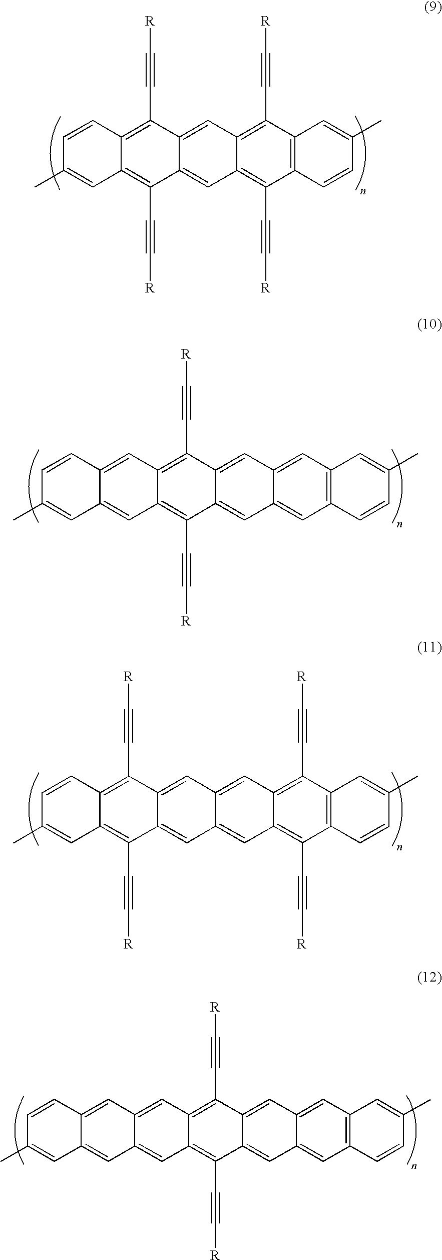
- a class of polyacenes is represented by the following formulas
- each R is as illustrated herein such as methyl, ethyl, propyl, butyl, pentyl, hexyl, heptyl, octyl, nonyl, decyl, undecyl, dodecyl, tridecyl, tetradecyl, pentadecyl, hexadecyl, heptadecyl, octadecyl, phenyl, methylphenyl(tolyl), ethylphenyl, propylphenyl, butylphenyl, pentylphenyl, hexylphenyl, heptylphenyl, octylphenyl, nonylphenyl, decylphenyl, undecylphenyl, dodecylphenyl, tridecylphenyl, tetradecylphenyl, pentadecyl,
- an electronic device comprising a semiconductive material containing a polyacene of Formula (I) wherein R is a suitable hydrocarbon, which may or may not be substituted, such as alkyl, aryl, and the like, and with, for example, from about 1 to about 40 carbon atoms, and more specifically, from about 10 to about 25 carbon atoms, such as methyl, ethyl, propyl, butyl, pentyl, hexyl, heptyl, octyl, nonyl, decyl, undecyl, dodecyl, tridecyl, tetradecyl, pentadecyl, hexadecyl, heptadecyl, octadecyl, nonadecyl, or eicosanyl, phenyl, methylphenyl(tolyl), ethylphenyl, propylphenyl, buty
- an electronic device comprising a semiconductive material containing a polyacene of Formula (I)
- R is a suitable hydrocarbon, a halogen, or a heteroatom containing group; each R′ and R′′ are independently a suitable hydrocarbon, a heteroatom containing group, or a halogen; x and y each represent the number of groups or rings; a and b each independently represent the number of groups; and n represents the number of repeating units; a device wherein the hydrocarbon is methyl, ethyl, propyl, butyl, pentyl, hexyl, heptyl, octyl, nonyl, decyl, undecyl, dodecyl, tridecyl, tetradecyl, pentadecyl, hexadecyl, heptadecyl, octadecyl, phenyl, methylphenyl(tolyl), ethylphenyl, propylphenyl, butylphenyl, pentylpheny
- R is a suitable hydrocarbon, a halogen or a heteroatom containing group
- each R′ and R′′ are independently a suitable hydrocarbon, a heteroatom containing group or a halogen
- x and y each represent the number of groups
- a and b each independently represent the number of rings
- n represents the number of repeating units
- poly(bis (ethynyl)anthracene)s can be accomplished by, for example, the dehalogenative coupling polymerization of 2,6-dibromo-9,10-bis(ethynyl)anthracenes in the presence of zinc, nickel(II) chloride, 2,2′-dipyridil, and triphenylphosphine in dimethylacetamide (DMAc) at elevated temperatures of, for example, 80° C. for a suitable timer period like 24 hours as illustrated in Scheme 2
- DMAc dimethylacetamide
- each R is as illustrated herein, and n is a number of from about 20 to about 100.
- the polyacenes in embodiments are soluble or substantially soluble wherein soluble refers, for example, to when the polymer can be dissolved in a solvent to form a solution with a concentration of at least 0.1 percent by weight to about 95 weight percent of the polymer; above this value, the polymer solution is sufficient to generate thin film transistors and other electronic devices in common coating solvents, for example, in embodiments they possess a solubility of at least about 0.1 percent by weight, and more specifically, from about 0.3 percent to about 5 percent by weight in such solvents as methylene chloride, 1,2-dichloroethane, tetrahydrofuran, toluene, xylene, mesitylene, chlorobenzene, dichlorobenzene, and the like.
- solvents as methylene chloride, 1,2-dichloroethane, tetrahydrofuran, toluene, xylene, mesitylene, chlorobenzene, dichlorobenzene, and the like.
- the polyacenes of the present disclosure when fabricated as semiconductor channel layers in TFT devices, provide a conductivity of, for example, from about 10 ⁇ 9 S/cm to about 10 ⁇ 4 S/cm, and more specifically, from about 10 ⁇ 8 S/cm to about 10 ⁇ 5 S/cm as determined by conventional four-probe conductivity measurements.
- the polyacenes when fabricated from solutions as thin films of, for example, from about 10 nanometers to about 500 nanometers, or from about 50 to about 300 nanometers in thickness materials, are more stable in ambient conditions than similar devices fabricated from acenes like pentacene.
- the aforementioned polyacene materials and devices are generally stable for a number of weeks rather than days or hours as is the situation with poly(3-alkylthiophene-2,5-diyl) after exposure to ambient oxygen, thus the devices fabricated from the polyacenes in embodiments of the present disclosure can provide higher current on/off ratios, and their performance characteristics do not substantially change as rapidly as poly(3-alkylthiophene-2,5-diyl) when no rigorous procedural precautions have been taken to exclude ambient oxygen during material preparation, device fabrication, and evaluation.
- polyacenes stability of the present disclosure in embodiments against oxidative doping, particularly for low cost device manufacturing, do not usually have to be handled in an inert atmosphere and the processes thereof are, therefore, simpler and more cost effective, and the fabrication thereof can be applied to large scale production processes.
- FIG. 1 there is schematically illustrated a TFT configuration 10 comprised of a substrate 16 , in contact therewith a metal contact 18 (gate electrode), and a layer of an insulating dielectric layer 14 , with the gate electrode having a portion thereof or the entire gate in contact with the dielectric layer 14 on top of which layer 14 two metal contacts, 20 and 22 (source and drain electrodes), are deposited.
- a metal contact 18 gate electrode
- a layer of an insulating dielectric layer 14 Over and between the metal contacts 20 and 22 is the polyacene layer of poly(9,10-didecynylanthracene-2,6-diyl) (1a), 12.
- the gate electrode can be included in the substrate, in the dielectric layer, and the like throughout.
- FIG. 2 schematically illustrates another TFT configuration 30 comprised of a substrate 36 , a gate electrode 38 , a source electrode 40 , and a drain electrode 42 , an insulating dielectric layer 34 , and the polyacene semiconductor layer 32 of FIG. 1 .
- FIG. 3 schematically illustrates a further TFT configuration 50 comprised of a heavily n-doped silicon wafer 56 , which can act as a gate electrode, a thermally grown silicon oxide dielectric layer 54 , the polyacene of FIG. 1 , 52 , on top of which are deposited a source electrode 60 and a drain electrode 62 ; and a gate electrode contact 64 .
- FIG. 4 schematically illustrates a TFT configuration 70 comprised of substrate 76 , a gate electrode 78 , a source electrode 80 , a drain electrode 82 , the polyacene semiconductor layer 72 of FIG. 1 , and an insulating dielectric layer 74 .
- TFT devices are envisioned, reference for example known TFT devices.
- an optional protecting layer may be incorporated on top of each of the transistor configurations of FIGS. 1 , 2 , 3 and 4 .
- the insulating dielectric layer 74 may also function as a protecting layer.
- the substrate layer may generally be a silicon material inclusive of various appropriate forms of silicon, a glass plate, a plastic film or a sheet, and the like depending on the intended applications.
- a plastic substrate such as for example polyester, polycarbonate, polyimide sheets, and the like, may be selected.
- the thickness of the substrate may be, for example, from about 10 micrometers to over 10 millimeters with a specific thickness being from about 50 to about 100 micrometers, especially for a flexible plastic substrate, and from about 1 to about 10 millimeters for a rigid substrate, such as glass or silicon.
- the insulating dielectric layer which can separate the gate electrode from the source and drain electrodes, and in contact with the semiconductor layer, can generally be an inorganic material film, an organic polymer film, or an organic-inorganic composite film.
- the thickness of the dielectric layer is, for example, from about 10 nanometers to about 1 micrometer with a more specific thickness being about 100 nanometers to about 500 nanometers.
- Illustrative examples of inorganic materials suitable as the dielectric layer include silicon oxide, silicon nitride, aluminum oxide, barium titanate, barium zirconate titanate, and the like; illustrative examples of organic polymers for the dielectric layer include polyesters, polycarbonates, poly(vinyl phenol), polyimides, polystyrene, poly(methacrylate)s, poly(acrylate)s, epoxy resin, and the like; and illustrative examples of inorganic-organic composite materials include nanometer-sized metal oxide particles dispersed in polymers, such as polyester, polyimide, epoxy resin and the like.
- the insulating dielectric layer is generally of a thickness of from about 50 nanometers to about 500 nanometers depending on the dielectric constant of the dielectric material used. More specifically, the dielectric material has a dielectric constant of, for example, at least about 3, thus a suitable dielectric thickness of about 300 nanometers can provide a desirable capacitance, for example, of about 10 ⁇ 9 to about 10 ⁇ 7 F/cm 2 .
- the active semiconductor layer comprised of the polyacenes illustrated herein, and wherein the thickness of this layer is generally, for example, about 10 nanometers to about 1 micrometer, or about 40 to about 100 nanometers.
- This layer can generally be fabricated by solution process polyacenes of the present disclosure.
- the gate electrode can be a thin metal film, a conducting polymer film, a conducting film generated from a conducting ink or paste, or the substrate itself (for example heavily doped silicon).
- gate electrode materials include, but are not limited to aluminum, gold, chromium, indium tin oxide, conducting polymers, such as polystyrene sulfonate-doped poly(3,4-ethylenedioxythiophene) (PSS/PEDOT), a conducting ink/paste comprised of carbon black/graphite or colloidal silver dispersion contained in a polymer binder, such as Electrodag available from Acheson Colloids Company, and silver filled electrically conductive thermoplastic ink available from Noelle Industries, and the like.
- the gate layer can be prepared by vacuum evaporation, sputtering of metals or conductive metal oxides, coating from conducting polymer solutions or conducting inks or dispersions by spin coating, casting or printing.
- the thickness of the gate electrode layer is, for example, from about 10 nanometers to about 10 micrometers, and a specific thickness is, for example, from about 10 to about 200 nanometers for metal films and about 1 to about 10 micrometers for polymer conductors.
- the source and drain electrode layer can be fabricated from materials which provide a low resistance ohmic contact to the semiconductor layer.
- Typical materials suitable for use as source and drain electrodes include those of the gate electrode materials, such as gold, silver, nickel, aluminum, platinum, conducting polymers, and conducting inks.
- Typical thickness of this layer is about, for example, from about 40 nanometers to about 1 micrometer with the more specific thickness being about 100 to about 400 nanometers.
- the TFT devices contain a semiconductor channel with a width W and length L.
- the semiconductor channel width may be, for example, from about 10 micrometers to about 5 millimeters, with a specific channel width being about 100 micrometers to about 1 millimeter.
- the semiconductor channel length may be, for example, from about 1 micrometer to about 1 millimeter with a more specific channel length being from about 5 micrometers to about 100 micrometers.
- the source electrode is grounded and a bias voltage of generally, for example, about 0 volt to about ⁇ 80 volts is applied to the drain electrode to collect the charge carriers transported across the semiconductor channel when a voltage of generally about +10 volts to about ⁇ 80 volts is applied to the gate electrode.
- the ethynyl groups function primarily to minimize or avoid instability because of exposure to oxygen, and thus increase the oxidative stability of the polyacenes in solution under ambient conditions, and the R and R′′ substituents, such as alkyl, permit the solubility of these polymers in common solvents, such as ethylene chloride, tetrahydrofuran, toluene, chlorobenzene, dichlorobenzene, and the like.
Landscapes
- Chemical & Material Sciences (AREA)
- Health & Medical Sciences (AREA)
- Chemical Kinetics & Catalysis (AREA)
- Medicinal Chemistry (AREA)
- Polymers & Plastics (AREA)
- Organic Chemistry (AREA)
- Engineering & Computer Science (AREA)
- Materials Engineering (AREA)
- Thin Film Transistor (AREA)
Abstract

wherein R is a suitable hydrocarbon, a halogen, or a heteroatom containing group; each R′ and R″ are independently a suitable hydrocarbon, a heteroatom containing group, or a halogen; a represents a number of benzene rings on a left side of the central benzene ring; b represents a number of benzene rings on a right side of the central benzene ring; x represents a total number of R′ groups on the left side of the central benzene ring; y represents a total number of R″ groups on the right side of the central benzene ring; and n represents the number of repeating units and is from 2 to about 5,000.
Description

wherein, for example, each R is a hydrocarbon group with, for example, 1 to about 40 carbon atoms; a heteroatom containing group with, for example, 1 to about 60 carbon atoms; x and y each represent the number of groups, and can be, for example, from zero to about 12, and more specifically, wherein each x and y are from about zero to about 6; a and b each independently represent the number of rings, and more specifically, wherein a is from zero to about 6 and b is from zero to about 6; n represents the number of repeating units, such as for example, n is a number of from about 2 to about 5,000, and more specifically, from about 2 to about 1,000 or from about 5 to about 500; and the sum of x and y can be, for example, from zero to about 12, and the sum of a and b can be, for example, from about 2 to about 6.


wherein each R is as illustrated herein such as methyl, ethyl, propyl, butyl, pentyl, hexyl, heptyl, octyl, nonyl, decyl, undecyl, dodecyl, tridecyl, tetradecyl, pentadecyl, hexadecyl, heptadecyl, octadecyl, phenyl, methylphenyl(tolyl), ethylphenyl, propylphenyl, butylphenyl, pentylphenyl, hexylphenyl, heptylphenyl, octylphenyl, nonylphenyl, decylphenyl, undecylphenyl, dodecylphenyl, tridecylphenyl, tetradecylphenyl, pentadecylphenyl, hexadecylphenyl, heptadecylphenyl, or octadecylphenyl; a heteroatom containing group with about 1 to about 60 carbon atoms, such as CN, thiazolyl, thienyl, furyl, pyridyl, trimethylsilyl, triethylsilyl, tripropylsilyl, tributylsilyl, tripentylsilyl, trihexylsilyl, triphenylsilyl, tritolylsilyl, tri(ethylphenyl)silyl, tri(propylphenyl)silyl, tri(butylphenyl)silyl, tri(pentylphenyl)silyl, tri(hexylphenyl)silyl, tri(heptylphenyl)silyl, tri(octylphenyl)silyl, tri(nonylphenyl)silyl, tri(decylphenyl)silyl, or tri(dodecylphenyl)silyl; and wherein n is the number of repeating units in the polymer, such as, for example, 2 to about 5,000, and more specifically, from about 2 to about 1,000 or from about 20 to about 100.

wherein R is a suitable hydrocarbon, a halogen, or a heteroatom containing group; each R′ and R″ are independently a suitable hydrocarbon, a heteroatom containing group, or a halogen; x and y each represent the number of groups or rings; a and b each independently represent the number of groups; and n represents the number of repeating units; a device wherein the hydrocarbon is methyl, ethyl, propyl, butyl, pentyl, hexyl, heptyl, octyl, nonyl, decyl, undecyl, dodecyl, tridecyl, tetradecyl, pentadecyl, hexadecyl, heptadecyl, octadecyl, phenyl, methylphenyl(tolyl), ethylphenyl, propylphenyl, butylphenyl, pentylphenyl, hexylphenyl, heptylphenyl, octylphenyl, nonylphenyl, decylphenyl, undecylphenyl, dodecylphenyl, tridecylphenyl, tetradecylphenyl, pentadecylphenyl, hexadecylphenyl, heptadecylphenyl, or octadecylphenyl; a device wherein x and y is independently a number of from zero to about 12; each a and b is a number of from zero to about 3; and n represents a number of from about 2 to about 1,000; a device wherein each x and y is independently a number of from about zero to about 6; each a and b is a number of from about zero to about 3, and n represents a number of from about 10 to about 200; a device wherein each x and y is independently a number of from zero to about 4; each a and b is a number of from zero to about 4; and n represents a number of from about 20 to about 100; a device wherein at least one of R, R′, or R″ is methyl, ethyl, propyl, butyl, pentyl, hexyl, heptyl, octyl, nonyl, decyl, undecyl, dodecyl, tridecyl, tetradecyl, pentadecyl, hexadecyl, heptadecyl, octadecyl, nonadecyl, eicosanyl, phenyl, methylphenyl(tolyl), ethylphenyl, propylphenyl, butylphenyl, pentylphenyl, hexylphenyl, heptylphenyl, octylphenyl, nonylphenyl, decylphenyl, undecylphenyl, dodecylphenyl, tridecylphenyl, tetradecylphenyl, pentadecylphenyl, hexadecylphenyl, heptadecylphenyl, octadecylphenyl; or thiazolyl, thienyl, furyl, pyridyl, trimethylsilyl, triethylsilyl, tripropylsilyl, tributylsilyl, tripentylsilyl, trihexylsilyl, triphenylsilyl, tritolylsilyl, tri(ethylphenyl)silyl, tri(propylphenyl)silyl, tri(butylphenyl)silyl, tri(pentylphenyl)silyl, tri(hexylphenyl)silyl, tri(heptylphenyl)silyl, tri(octylphenyl)silyl, tri(nonylphenyl)silyl, tri(decylphenyl)silyl, tri(dodecylphenyl)silyl, or mixtures thereof; a thin film transistor comprised of a substrate, a gate electrode, a gate dielectric layer, a source electrode and a drain electrode, and in contact with the source/drain electrodes and the gate dielectric layer a semiconductor layer comprised of a polyacene of the formula/structure

wherein R is a suitable hydrocarbon, a halogen or a heteroatom containing group; each R′ and R″ are independently a suitable hydrocarbon, a heteroatom containing group or a halogen; x and y each represent the number of groups; a and b each independently represent the number of rings; and n represents the number of repeating units; and in embodiments, there are disclosed processes for the preparation of polyacenes in accordance, for example, with the following reaction scheme (Scheme 1)

and more specifically, prepared by utilizing a dehalogenative coupling reaction of dihalogenated bis(ethynyl)acenes. More specifically, the preparation of poly(bis (ethynyl)anthracene)s can be accomplished by, for example, the dehalogenative coupling polymerization of 2,6-dibromo-9,10-bis(ethynyl)anthracenes in the presence of zinc, nickel(II) chloride, 2,2′-dipyridil, and triphenylphosphine in dimethylacetamide (DMAc) at elevated temperatures of, for example, 80° C. for a suitable timer period like 24 hours as illustrated in Scheme 2

whereas the monomer 2,6-dibromo-9,10-ethynylanthracene can be readily prepared by reacting 2,6-dibromoanthracene with ethynylmagnesium chloride, followed by reduction with tin(II) chloride (Scheme 2).

wherein each R is as illustrated herein, and n is a number of from about 20 to about 100.
Claims (32)


Priority Applications (1)
| Application Number | Priority Date | Filing Date | Title |
|---|---|---|---|
| US11/399,216 US7550760B2 (en) | 2006-04-06 | 2006-04-06 | Polyacenes and electronic devices generated therefrom |
Applications Claiming Priority (1)
| Application Number | Priority Date | Filing Date | Title |
|---|---|---|---|
| US11/399,216 US7550760B2 (en) | 2006-04-06 | 2006-04-06 | Polyacenes and electronic devices generated therefrom |
Publications (2)
| Publication Number | Publication Date |
|---|---|
| US20070252138A1 US20070252138A1 (en) | 2007-11-01 |
| US7550760B2 true US7550760B2 (en) | 2009-06-23 |
Family
ID=38647500
Family Applications (1)
| Application Number | Title | Priority Date | Filing Date |
|---|---|---|---|
| US11/399,216 Active 2026-10-29 US7550760B2 (en) | 2006-04-06 | 2006-04-06 | Polyacenes and electronic devices generated therefrom |
Country Status (1)
| Country | Link |
|---|---|
| US (1) | US7550760B2 (en) |
Families Citing this family (3)
| Publication number | Priority date | Publication date | Assignee | Title |
|---|---|---|---|---|
| US7558186B2 (en) | 2007-01-02 | 2009-07-07 | International Business Machines Corporation | High density data storage medium, method and device |
| US20080159114A1 (en) * | 2007-01-02 | 2008-07-03 | Dipietro Richard Anthony | High density data storage medium, method and device |
| DE102009030847A1 (en) * | 2009-06-26 | 2010-12-30 | Merck Patent Gmbh | Polymers containing substituted Anthracenyleinheiten, blends containing these polymers and devices containing these polymers or blends |
Citations (8)
| Publication number | Priority date | Publication date | Assignee | Title |
|---|---|---|---|---|
| US5619357A (en) | 1995-06-06 | 1997-04-08 | International Business Machines Corporation | Flat panel display containing black matrix polymer |
| US5777070A (en) | 1997-10-23 | 1998-07-07 | The Dow Chemical Company | Process for preparing conjugated polymers |
| US5969376A (en) | 1996-08-23 | 1999-10-19 | Lucent Technologies Inc. | Organic thin film transistor having a phthalocyanine semiconductor layer |
| US6107117A (en) | 1996-12-20 | 2000-08-22 | Lucent Technologies Inc. | Method of making an organic thin film transistor |
| US6770904B2 (en) | 2002-01-11 | 2004-08-03 | Xerox Corporation | Polythiophenes and electronic devices generated therefrom |
| US20050017311A1 (en) | 2002-01-11 | 2005-01-27 | Xerox Corporation | Polythiophenes and electronic devices generated therefrom |
| US20050215732A1 (en) * | 2004-03-23 | 2005-09-29 | Fuji Photo Film Co., Ltd. | Composition for film formation, coating solution containing the same and electronic device having insulating film obtained by using the coating solution |
| US20060131570A1 (en) * | 2004-11-02 | 2006-06-22 | Hong Meng | Substituted anthracenes and electronic devices containing the substituted anthracenes |
-
2006
- 2006-04-06 US US11/399,216 patent/US7550760B2/en active Active
Patent Citations (9)
| Publication number | Priority date | Publication date | Assignee | Title |
|---|---|---|---|---|
| US5619357A (en) | 1995-06-06 | 1997-04-08 | International Business Machines Corporation | Flat panel display containing black matrix polymer |
| US5969376A (en) | 1996-08-23 | 1999-10-19 | Lucent Technologies Inc. | Organic thin film transistor having a phthalocyanine semiconductor layer |
| US6150191A (en) | 1996-08-23 | 2000-11-21 | Lucent Technologies Inc. | Method of making an organic thin film transistor and article made by the method |
| US6107117A (en) | 1996-12-20 | 2000-08-22 | Lucent Technologies Inc. | Method of making an organic thin film transistor |
| US5777070A (en) | 1997-10-23 | 1998-07-07 | The Dow Chemical Company | Process for preparing conjugated polymers |
| US6770904B2 (en) | 2002-01-11 | 2004-08-03 | Xerox Corporation | Polythiophenes and electronic devices generated therefrom |
| US20050017311A1 (en) | 2002-01-11 | 2005-01-27 | Xerox Corporation | Polythiophenes and electronic devices generated therefrom |
| US20050215732A1 (en) * | 2004-03-23 | 2005-09-29 | Fuji Photo Film Co., Ltd. | Composition for film formation, coating solution containing the same and electronic device having insulating film obtained by using the coating solution |
| US20060131570A1 (en) * | 2004-11-02 | 2006-06-22 | Hong Meng | Substituted anthracenes and electronic devices containing the substituted anthracenes |
Non-Patent Citations (5)
| Title |
|---|
| Huang, D.H., et al., "Conjugated Polymers Based on Phenothiazine and Fluorene in Light-Emitting Diodes and Field Effect Transistors", Chem. Mater. 2004, 16, 1298-1303. |
| Ong, Beng, et al., U.S. Appl. No. 11/011,678, filed Dec. 14, 2004 on Compound with Indolocarbazole Moieties and Devices Containing Such Compound. |
| Ong, Beng, et al., U.S. Appl. No. 11/167,512, filed Jun. 27, 2005 on Compound with Indolocarbazole Moieties and Devices Containing Such Compound. |
| See the "Cross Reference to Related Applications" on pp. 1 and 2 of the Specification Being Filed Concurrently. |
| Zhu, Y., et al, "Phenoxazine-Based Conjugated Polymers: A New Class of Organic Semiconductors for Field-Effect Transistors", Macromolecules 2005, 38, 7983-7991. |
Also Published As
| Publication number | Publication date |
|---|---|
| US20070252138A1 (en) | 2007-11-01 |
Similar Documents
| Publication | Publication Date | Title |
|---|---|---|
| US7767999B2 (en) | Polythiophenes and devices thereof | |
| EP1843410B1 (en) | Functionalized heteroacenes and electronic devices generated therefrom | |
| US20060041103A1 (en) | Polythiophenes and devices thereof | |
| US7994497B2 (en) | Poly[bis(ethynyl)heteroacene]s and electronic devices generated therefrom | |
| US7557370B2 (en) | Heteroacene polymers and electronic devices generated therefrom | |
| EP1849812B1 (en) | Linked arylamine polymers and electronic devices generated therefrom | |
| CA2583047C (en) | Semiconductors and electronic devices generated therefrom | |
| US8049205B2 (en) | Poly(alkynylthiophene)s and electronic devices generated therefrom | |
| US7550760B2 (en) | Polyacenes and electronic devices generated therefrom | |
| US7795373B2 (en) | Ethynylene acene polymers | |
| US7615607B2 (en) | Semiconductor polymers | |
| US8334391B2 (en) | Functionalized heteroacenes | |
| US7847052B2 (en) | Linked arylamine polymers | |
| US7517476B2 (en) | Polydiazaacenes | |
| US7586120B2 (en) | Ethynylene acene polymers and electronic devices generated therefrom | |
| US7517477B2 (en) | Polydiazaacenes and electronic devices generated therefrom | |
| US7705111B2 (en) | Poly(alkynylthiophene)s |
Legal Events
| Date | Code | Title | Description |
|---|---|---|---|
| AS | Assignment |
Owner name: XEROX CORPORATION, CONNECTICUT Free format text: ASSIGNMENT OF ASSIGNORS INTEREST;ASSIGNORS:LI, YUNING;LIU, PING;WU, YILIANG;AND OTHERS;REEL/FRAME:017771/0456 Effective date: 20060403 |
|
| FEPP | Fee payment procedure |
Free format text: PAYOR NUMBER ASSIGNED (ORIGINAL EVENT CODE: ASPN); ENTITY STATUS OF PATENT OWNER: LARGE ENTITY |
|
| STCF | Information on status: patent grant |
Free format text: PATENTED CASE |
|
| FPAY | Fee payment |
Year of fee payment: 4 |
|
| CC | Certificate of correction | ||
| FPAY | Fee payment |
Year of fee payment: 8 |
|
| MAFP | Maintenance fee payment |
Free format text: PAYMENT OF MAINTENANCE FEE, 12TH YEAR, LARGE ENTITY (ORIGINAL EVENT CODE: M1553); ENTITY STATUS OF PATENT OWNER: LARGE ENTITY Year of fee payment: 12 |
|
| AS | Assignment |
Owner name: CITIBANK, N.A., AS AGENT, DELAWARE Free format text: SECURITY INTEREST;ASSIGNOR:XEROX CORPORATION;REEL/FRAME:062740/0214 Effective date: 20221107 |
|
| AS | Assignment |
Owner name: XEROX CORPORATION, CONNECTICUT Free format text: RELEASE OF SECURITY INTEREST IN PATENTS AT R/F 062740/0214;ASSIGNOR:CITIBANK, N.A., AS AGENT;REEL/FRAME:063694/0122 Effective date: 20230517 |
|
| AS | Assignment |
Owner name: CITIBANK, N.A., AS COLLATERAL AGENT, NEW YORK Free format text: SECURITY INTEREST;ASSIGNOR:XEROX CORPORATION;REEL/FRAME:064760/0389 Effective date: 20230621 |
|
| AS | Assignment |
Owner name: JEFFERIES FINANCE LLC, AS COLLATERAL AGENT, NEW YORK Free format text: SECURITY INTEREST;ASSIGNOR:XEROX CORPORATION;REEL/FRAME:065628/0019 Effective date: 20231117 |
|
| AS | Assignment |
Owner name: XEROX CORPORATION, CONNECTICUT Free format text: TERMINATION AND RELEASE OF SECURITY INTEREST IN PATENTS RECORDED AT RF 064760/0389;ASSIGNOR:CITIBANK, N.A., AS COLLATERAL AGENT;REEL/FRAME:068261/0001 Effective date: 20240206 |
|
| AS | Assignment |
Owner name: U.S. BANK TRUST COMPANY, NATIONAL ASSOCIATION, AS COLLATERAL AGENT, CONNECTICUT Free format text: FIRST LIEN NOTES PATENT SECURITY AGREEMENT;ASSIGNOR:XEROX CORPORATION;REEL/FRAME:070824/0001 Effective date: 20250411 |
|
| AS | Assignment |
Owner name: U.S. BANK TRUST COMPANY, NATIONAL ASSOCIATION, AS COLLATERAL AGENT, CONNECTICUT Free format text: SECOND LIEN NOTES PATENT SECURITY AGREEMENT;ASSIGNOR:XEROX CORPORATION;REEL/FRAME:071785/0550 Effective date: 20250701 |