US7544556B1 - Process for forming CMOS devices using removable spacers - Google Patents
Process for forming CMOS devices using removable spacers Download PDFInfo
- Publication number
- US7544556B1 US7544556B1 US10/986,636 US98663604A US7544556B1 US 7544556 B1 US7544556 B1 US 7544556B1 US 98663604 A US98663604 A US 98663604A US 7544556 B1 US7544556 B1 US 7544556B1
- Authority
- US
- United States
- Prior art keywords
- layer
- spacers
- implant regions
- oxide
- source
- Prior art date
- Legal status (The legal status is an assumption and is not a legal conclusion. Google has not performed a legal analysis and makes no representation as to the accuracy of the status listed.)
- Expired - Fee Related, expires
Links
Images


Classifications
-
- H—ELECTRICITY
- H10—SEMICONDUCTOR DEVICES; ELECTRIC SOLID-STATE DEVICES NOT OTHERWISE PROVIDED FOR
- H10D—INORGANIC ELECTRIC SEMICONDUCTOR DEVICES
- H10D64/00—Electrodes of devices having potential barriers
- H10D64/01—Manufacture or treatment
- H10D64/011—Manufacture or treatment of electrodes ohmically coupled to a semiconductor
- H10D64/0111—Manufacture or treatment of electrodes ohmically coupled to a semiconductor to Group IV semiconductors
-
- H—ELECTRICITY
- H10—SEMICONDUCTOR DEVICES; ELECTRIC SOLID-STATE DEVICES NOT OTHERWISE PROVIDED FOR
- H10D—INORGANIC ELECTRIC SEMICONDUCTOR DEVICES
- H10D84/00—Integrated devices formed in or on semiconductor substrates that comprise only semiconducting layers, e.g. on Si wafers or on GaAs-on-Si wafers
- H10D84/01—Manufacture or treatment
- H10D84/0123—Integrating together multiple components covered by H10D12/00 or H10D30/00, e.g. integrating multiple IGBTs
- H10D84/0126—Integrating together multiple components covered by H10D12/00 or H10D30/00, e.g. integrating multiple IGBTs the components including insulated gates, e.g. IGFETs
- H10D84/0147—Manufacturing their gate sidewall spacers
-
- H—ELECTRICITY
- H10—SEMICONDUCTOR DEVICES; ELECTRIC SOLID-STATE DEVICES NOT OTHERWISE PROVIDED FOR
- H10D—INORGANIC ELECTRIC SEMICONDUCTOR DEVICES
- H10D84/00—Integrated devices formed in or on semiconductor substrates that comprise only semiconducting layers, e.g. on Si wafers or on GaAs-on-Si wafers
- H10D84/01—Manufacture or treatment
- H10D84/0123—Integrating together multiple components covered by H10D12/00 or H10D30/00, e.g. integrating multiple IGBTs
- H10D84/0126—Integrating together multiple components covered by H10D12/00 or H10D30/00, e.g. integrating multiple IGBTs the components including insulated gates, e.g. IGFETs
- H10D84/0149—Manufacturing their interconnections or electrodes, e.g. source or drain electrodes
-
- H—ELECTRICITY
- H10—SEMICONDUCTOR DEVICES; ELECTRIC SOLID-STATE DEVICES NOT OTHERWISE PROVIDED FOR
- H10D—INORGANIC ELECTRIC SEMICONDUCTOR DEVICES
- H10D84/00—Integrated devices formed in or on semiconductor substrates that comprise only semiconducting layers, e.g. on Si wafers or on GaAs-on-Si wafers
- H10D84/01—Manufacture or treatment
- H10D84/02—Manufacture or treatment characterised by using material-based technologies
- H10D84/03—Manufacture or treatment characterised by using material-based technologies using Group IV technology, e.g. silicon technology or silicon-carbide [SiC] technology
- H10D84/038—Manufacture or treatment characterised by using material-based technologies using Group IV technology, e.g. silicon technology or silicon-carbide [SiC] technology using silicon technology, e.g. SiGe
-
- H—ELECTRICITY
- H10—SEMICONDUCTOR DEVICES; ELECTRIC SOLID-STATE DEVICES NOT OTHERWISE PROVIDED FOR
- H10W—GENERIC PACKAGES, INTERCONNECTIONS, CONNECTORS OR OTHER CONSTRUCTIONAL DETAILS OF DEVICES COVERED BY CLASS H10
- H10W20/00—Interconnections in chips, wafers or substrates
- H10W20/01—Manufacture or treatment
- H10W20/031—Manufacture or treatment of conductive parts of the interconnections
- H10W20/069—Manufacture or treatment of conductive parts of the interconnections by forming self-aligned vias or self-aligned contact plugs
-
- H—ELECTRICITY
- H10—SEMICONDUCTOR DEVICES; ELECTRIC SOLID-STATE DEVICES NOT OTHERWISE PROVIDED FOR
- H10D—INORGANIC ELECTRIC SEMICONDUCTOR DEVICES
- H10D84/00—Integrated devices formed in or on semiconductor substrates that comprise only semiconducting layers, e.g. on Si wafers or on GaAs-on-Si wafers
- H10D84/01—Manufacture or treatment
- H10D84/0123—Integrating together multiple components covered by H10D12/00 or H10D30/00, e.g. integrating multiple IGBTs
- H10D84/0126—Integrating together multiple components covered by H10D12/00 or H10D30/00, e.g. integrating multiple IGBTs the components including insulated gates, e.g. IGFETs
- H10D84/013—Manufacturing their source or drain regions, e.g. silicided source or drain regions
- H10D84/0133—Manufacturing common source or drain regions between multiple IGFETs
Definitions
- the present invention relates to the field of semiconductor devices. More particularly, the present invention relates to Complimentary Metal-Oxide Semiconductor (CMOS) manufacturing processes.
- CMOS Complimentary Metal-Oxide Semiconductor
- CMOS complementary Metal-Oxide Semiconductor
- disposable dielectric spacers are sometimes used to define the heavily doped contact region of a source/drain structure.
- a first implant is performed prior to forming the first spacer. This first implant forms lightly-doped drain (L DD ) regions.
- L DD lightly-doped drain
- the L-shaped permanent spacer and the disposable spacer are then formed, with the disposable spacer overlying the L-shaped spacer.
- a second implant process is then performed so as to form the heavily doped contact region.
- the disposable spacer is then removed, leaving the L-shaped spacer. This process works well when there is sufficient space between adjacent gate structures.
- the vertical or nearly-vertical slope of the L-shaped spacer causes voids to form during deposition of the pre-metal dielectric layer. These voids in the pre-metal dielectric layer can lead to bridging defects in the subsequently formed contacts.
- the width of conventional L-shaped spacers takes up valuable space on the semiconductor surface, limiting size reduction of closely-spaced CMOS structures.
- CMOS devices that give good gap-fill characteristics between adjacent gate structures. Also, there is a need for CMOS devices that do not have bridging defects.
- the present invention meets the above needs.
- CMOS Complimentary Metal Oxide Semiconductor
- a process for forming Complimentary Metal Oxide Semiconductor (CMOS) devices is disclosed in which disposable spacers are used to obtain a structure having improved gap-fill characteristics.
- gate film stacks are formed on the substrate.
- a shallow implant process is then performed so as to form shallow source/drain implant regions.
- a layer of oxide and a layer of silicon nitride are deposited and etched to form a first set of spacers that extend on opposite sides of the gate film stacks.
- a second implant is then performed so as to form intermediate source/drain implant regions.
- a set of disposable spacers are then formed that extend on opposite sides of each of the gate film stacks.
- a third implant process is then performed so as to form deep source/drain implant regions adjoining each of the disposable spacers. The disposable spacers are then removed.
- the resulting structure has sidewalls that are disposed at an angle greater than ninety degrees relative to the substrate.
- This sloped profile gives better gap-fill characteristics than prior art processes in which L-shaped spacers are used that have vertical sidewalls. Thereby, fewer voids are formed in the dielectric film, reducing the occurrence of bridging defects.
- the first set of spacers have a slope that is approximately triangular, and a width that is less than the width of L-shaped spacers that are used in prior art CMOS processes that utilize disposable spacers. Accordingly, once the disposable spacers are removed, there is more available space between adjacent gate film stacks, allowing for locating gate film stacks closer together than is possible in conventional prior art processes in which wider L-shaped spacers are used.
- FIG. 1 illustrates a process for forming a CMOS device using removable spacers in accordance with an embodiment of the present invention.
- FIG. 2 shows a semiconductor substrate over which a dielectric layer and two gate film stacks have been formed, after a first implant has been performed so as to form shallow source/drain regions in accordance with an embodiment of the present invention.
- FIG. 3 shows the structure of FIG. 2 after a layer of oxide and a layer of silicon nitride have been deposited over the semiconductor substrate in accordance with an embodiment of the present invention.
- FIG. 4 shows the structure of FIG. 3 after an etch process has been performed so as to remove portions of the oxide layer and the silicon nitride layer to form a first set of spacers, and after an implant process has been performed so as to form intermediate source/drain regions in accordance with an embodiment of the present invention.
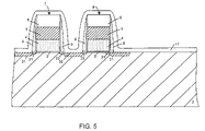
- FIG. 5 shows the structure of FIG. 4 after a dielectric layer has been deposited thereover in accordance with an embodiment of the present invention.
- FIG. 6 shows the structure of FIG. 5 after an etch process has been performed to selectively remove a portion of the dielectric layer, forming dielectric spacers that extend on each side of each gate film stack and after an implant process has been performed so as to form primary source/drain regions in accordance with an embodiment of the present invention.
- FIG. 7 shows the structure of FIG. 6 after removal of the disposable spacers in accordance with an embodiment of the present invention.
- FIG. 8 shows the structure of FIG. 7 after a barrier layer has been deposited and after a pre-metal dielectric film has been formed in accordance with an embodiment of the present invention.
- FIG. 9 shows the structure of FIG. 8 after a self-aligned contact has been formed that extends through the pre-metal dielectric film, the barrier layer, and the gate dielectric layer in accordance with an embodiment of the present invention.
- FIG. 1 illustrates a process for forming a CMOS structure using disposable spacers.
- a gate dielectric layer is formed over a semiconductor substrate.
- the gate dielectric layer can be formed by depositing or growing a thin layer (e.g., 10 to 80 Angstroms) of silicon dioxide (SiO 2 ), or other type of dielectric, on the semiconductor substrate.
- gate film stacks are formed over the gate dielectric layer.
- adjacent gate film stacks are formed that include a hard mask and one or more underlying layers.
- gate film stacks are formed that have a width of 1,400 Angstroms or less and have side surfaces that are approximately vertical.
- gate film stacks are identical and are closely spaced together, with adjacent gate film stacks separated by a distance of 2,000 Angstroms or less.
- exemplary gate film stacks 7 - 8 are shown to be formed that immediately overlie gate dielectric layer 3 . Patterning of gate film stacks 7 - 8 also removes portions of gate dielectric layer 3 so as to expose portions of semiconductor substrate 2 .
- Semiconductor substrate 2 can include isolation regions (e.g., using shallow trench isolation processing steps) or other device isolation structures, depending on the device requirements.
- Gate film stacks 7 - 8 include a conductive layer 4 , a silicide layer 5 , and a hard mask 6 .
- Conductive layer 4 includes one or more layers of conductive material that immediately overlie gate dielectric layer 3 . In one embodiment conductive layer 4 has a thickness of 500 to 2,000 Angstroms.
- Conductive layer 4 can be formed by depositing one or more layers of polysilicon using a chemical vapor deposition process. Alternatively, conductive layer 4 can be formed by depositing amorphous silicon in a furnace. In the present embodiment conductive layer 4 is a single layer of polysilicon that is deposited using a chemical vapor deposition process, and that has a thickness of approximately 650 Angstroms.
- silicide layer 5 can be formed of one or more layers of refractory metal silicide, with individual layers formed of cobalt silicide, tungsten silicide, titanium silicide, tantalum silicide, molybdeum silicide, niobium silicide, rhenium silicide, vanadium silicide, chromium silicide, zirconium silicide or hafnium silicide.
- Silicide layer can also be formed using non-refractory-metal silicides, or nonmetal silicides that have sufficient conductivity.
- silicide layer 5 is deposited using a Chemical Vapor Deposition (CVD) process and has a thickness of 600 to 1,000 Angstroms.
- silicide layer 5 is a single layer of tungsten silicide (WSi X ), that directly overlies conductive layer 4 , and that has a thickness of approximately 650 Angstroms.
- Hard mask 6 extends immediately over silicide layer 5 and can be formed of one or more layers of dielectric material.
- hard mask 6 is formed of a single layer of oxide (SiO 2 ), silicon nitride (SiN) or oxynitride (SiO x N y ) that has a thickness of 500 to 2,500 Angstroms.
- hard mask 6 can include multiple layers of material, with individual layers formed of oxide, silicon nitride or oxynitride.
- hard mask 6 can be formed using other dielectric materials that can be preferentially etched relative to silicide layer 5 .
- hard mask 6 is a single layer of silicon nitride having a thickness of approximately 2,125 Angstroms.
- an implant process is performed so as to form shallow source/drain implant regions.
- a masking structure is formed using photoresist that exposes portions of the substrate that are to be doped and an implant is performed so as to introduce impurities into the substrate.
- implant step 103 forms source and drain implant regions 21 - 22 .
- implant process 103 is performed using a low doping concentration and at a low energy level such that source/drain implant regions 21 - 22 are shallow and are lightly doped.
- region 22 is a common source/drain implant region that extends between gate film stacks 7 - 8 .
- implant region 22 can include two separate and distinct source and/or drain implant regions.
- a first set of spacers are formed as shown by steps 104 - 106 of FIG. 1 .
- an oxide layer is deposited.
- an oxide layer 15 is deposited over semiconductor substrate 2 using a Plasma Enhanced Chemical Vapor Deposition (PECVD) process such that oxide layer 15 immediately overlies gate film stacks 7 - 8 .
- PECVD Plasma Enhanced Chemical Vapor Deposition
- oxide layer 15 is a single layer of tetraethylorthosilicate (TEOS).
- TEOS tetraethylorthosilicate
- oxide layer 15 can also Undoped Silica Glass (USG).
- silicon nitride layer 16 is deposited using a Low Pressure Chemical Vapor Deposition (LPCVD) process such that silicon nitride layer 16 immediately overlies oxide layer 15 .
- oxide layer 15 has a thickness of 50 to 200 Angstroms and silicon nitride layer 16 has a thickness of 50 to 300 Angstroms.
- oxide layer 15 has a thickness of approximately 200 Angstroms and silicon nitride layer 16 has a thickness of approximately 300 Angstroms.
- the thickness of the oxide layer and the overlying silicon nitride layer will vary depending on the requirements of the particular fabrication process and the geometries and spacing of gate film stacks 7 - 8 .
- step 106 an etch process is performed so as to form a first set of spacers.
- the etch process of step 106 is a reactive ion etch that removes portions of layers 15 - 16 , forming spacers 9 that extend on opposite sides of each of gate film stacks 7 - 8 and immediately adjoin gate film stacks 7 - 8 .
- Spacers 9 have a shape that is approximately triangular, and extend laterally a width W 1 that is less than the width of conventional L-shaped spacers that are used in conventional prior art fabrication processes. In the present embodiment, the width W 1 of spacers 9 extends less than 400 angstroms.
- the reduced width W 1 of spacers 9 and the roughly triangular shape of spacers 9 can be obtained by tuning the power and timing of the reactive ion etch process. In one embodiment the reduced width W 1 and the roughly triangular shape of spacers 9 is obtained by using a high power setting and performing etch 106 for a short period of time.
- a second implant process is performed so as to form intermediate source/drain implant regions.
- a masking structure is formed using photoresist that exposes portions of the substrate that are to be doped and an implant is performed so as to introduce impurities into the substrate.
- implant step 107 forms source and drain implant regions 31 - 32 .
- implant process 107 is performed using a doping concentration that is higher than the doping concentration of step 103 and is performed at a higher energy level than the energy level used in step 103 , producing source/drain implant regions 31 - 32 having a depth that is greater than the depth of source/drain implant regions 21 - 22 , and a doping concentration that is greater than the doping concentration of source/drain implant regions 21 - 22 .
- region 32 is a common source/drain implant region that extends between gate film stacks 7 - 8 .
- source/drain implant region 32 could include two separate and distinct source and/or drain implant regions.
- source/drain implant regions 31 - 32 nearest gate film stacks 7 - 8 are defined by spacers 9 . More particularly, since spacers 9 extend a distance W 1 from the sides of gate film stacks 7 - 8 , the boundaries of source/drain implant regions 31 - 32 nearest gate film stacks 7 - 8 will also extend approximately a width W 1 from the sides of gate film stacks 7 - 8 .
- a dielectric layer is deposited.
- a dielectric layer 17 is deposited over semiconductor substrate 2 such that it immediately overlies portions of gate film stacks 7 - 8 and spacers 9 .
- dielectric layer 17 is a single layer of oxide that is deposited using a Plasma Enhanced Chemical Vapor Deposition (PECVD) process.
- PECVD Plasma Enhanced Chemical Vapor Deposition
- dielectric layer 17 is a single layer of phosphosilicate glass (PSG).
- PSG phosphosilicate glass
- dielectric layer 17 can also be doped oxide, borophosphosilica glass (BPSG), undoped silica glass (USG), borosilica glass (BSG) or other dielectric material that can be etched at a high etch rate.
- dielectric layer 17 can include multiple layers of material, with individual layers formed of doped oxide, BPSG, USG, BSG, PSG or oxynitride.
- dielectric layer 17 has a thickness of from 50 to 400 Angstroms.
- step 109 an etch process is performed so as to form a second set of spacers.
- the etch process of step 109 is a reactive ion etch that removes portions of dielectric layer 17 , forming disposable spacers 10 that immediately adjoin spacers 9 and that extend on opposite sides of gate film stacks 7 - 8 .
- disposable spacers 10 have a width at their base that is shown as width W 2 .
- dielectric layer 17 has a thickness prior to etch (step 109 ) of 400 Angstroms, forming spacers 9 having a thickness W 2 of approximately 300 Angstroms.
- the width W 2 will vary depending on the thickness of dielectric layer 17 prior to etch, and the deposition process that is used.
- an implant process is performed so as to form primary source/drain regions.
- a masking structure is formed using photoresist that exposes portions of the substrate that are to be doped and an implant is performed so as to introduce impurities into the substrate.
- implant step 110 forms primary source and drain implant regions 41 - 42 .
- implant process 110 is performed using a high doping concentration and at a high energy level such that source/drain implant regions 41 - 42 are deep and are heavily doped. Accordingly, the doping concentration and depth of source/drain implants 41 - 42 will be greater than the doping concentration and depth of both source/drain implant regions 21 - 22 and 31 - 32 .
- source/drain implant regions 41 - 42 nearest gate film stacks 7 - 8 are defined by disposable spacers 10 . More particularly, since spacers 10 extend a distance W 2 from the sides of gate film stacks 7 - 8 , the boundaries of source/drain implant regions 41 - 42 nearest gate film stacks 7 - 8 will also extend approximately a width W 2 from the sides of gate film stacks 7 - 8 .
- source/drain implant region 42 is a common source/drain implant region that extends between gate film stacks 7 - 8 . However, alternatively, source/drain implant region 42 could include two separate and distinct source and/or drain regions.
- FIG. 6 shows the completed source/drain regions formed by steps 101 - 110 of the present invention that includes shallow source/drain implant regions 21 - 22 , intermediate source/drain implant regions 31 - 32 and primary source/drain implant regions 41 - 42 .
- Shallow source/drain implant regions 21 - 22 extend from each side of gate film stacks 7 - 8 , and have a shallow depth relative to the depth of intermediate source/drain implant regions 31 - 32 and primary source/drain implant regions 41 - 42 .
- Primary source/drain implant regions 41 - 42 adjoin intermediate source/drain implant regions 31 - 32 and have a deep depth, with the depth of primary source/drain implant regions 41 - 42 being greater than the depth of shallow source/drain implant regions 21 - 22 and intermediate source/drain implant regions 31 - 32 .
- Intermediate source/drain implant regions 31 - 32 extend between shallow source/drain implant regions 21 - 22 and primary source/drain implant regions 41 - 42 , and have an intermediate-depth relative to the depth of shallow source/drain regions 21 - 22 and primary source/drain regions 41 - 42 .
- intermediate source/drain implant regions 31 - 32 will be greater than the depth of shallow source/drain implant regions 21 - 22 and will be less than the depth of primary source/drain implant regions 41 - 42 .
- the use of intermediate source drain implant regions 31 - 32 reduces the likelihood of charge tunneling, while not compromising drive current by having an unnecessarily high resistive region adjacent to the transistor channel.
- NMOS devices are formed that include N ⁇ source/drain implant regions 21 - 22 that have a depth of from 0.1 to 0.2 microns, N ⁇ source/drain implant regions 31 - 32 that have a depth of from 0.15 to 0.25 microns, and N+ source/drain implants 41 - 42 that have a depth of from 0.25 to 0.5 micron.
- PMOS devices can be formed having similar source/drain implant regions.
- step 111 The disposable spacers are removed as shown by step 111 .
- a wet etch is used to remove the disposable spacers.
- a hydrofluoric acid is used to remove disposable spacers 10 , giving the structure shown in FIG. 7 . It can be seen that step 111 removes all of disposable spacers 10 so as to expose that portion of semiconductor substrate 2 in which intermediate source/drain implant regions 31 - 32 are formed.
- an anneal process is performed so as to extend source/drain implant regions 21 - 22 , 31 - 32 and 41 - 42 .
- the anneal process can be performed by heating semiconductor substrate 2 in a furnace and can be performed either before or after step 111 .
- an anneal process can be performed later in the CMOS fabrication process.
- FIGS. 1-8 forms a CMOS structure that has good gap-fill characteristics. More particularly, the sides of spacers 9 that extend between gate film stacks 7 - 8 extend at an angle that is greater than ninety degrees relative to the top surface of semiconductor substrate 2 . This sloped profile gives better gap-fill characteristics than prior art processes in which L-shaped spacers are used that have vertical sidewalls. Thereby, fewer voids are formed in the subsequently-formed dielectric film, reducing the occurrence of bridging defects.
- spacers 9 (W 1 ) is less the width of conventional L-shaped spacers that are used in prior art CMOS processes that utilize disposable spacers, gate film stacks can be formed closer together than is allowed by conventional prior art processes in which L-shaped spacers are used.
- a self-aligned contact structure is formed that connects source drain implant region 42 to overlying circuitry.
- a barrier layer 13 is deposited over semiconductor substrate 2 .
- Barrier layer 13 can be one or more layers of dielectric material, with each layer formed of silicon nitride, silicon oxide, silicon oxynitride, or other dielectric material that can act as an etch stop relative to the material in pre-metal dielectric film 14 .
- barrier layer 13 is formed by depositing a single layer of silicon nitride, having a thickness of approximately 200 Angstroms.
- Pre-metal dielectric film 14 is then formed.
- dielectric film 14 extends over the entire semiconductor substrate and has a thickness such that it extends from 1,000 to 15,000 Angstroms over the top of gate film stacks 7 - 8 .
- Pre-metal dielectric film 14 can be one or more layers of dielectric material, with each layer formed of doped oxide, borophosphosilica glass (BPSG), undoped silica glass (USG), spin on glass (SOG), borosilica glass (BSG), phosphosilicate glass (PSG) or tetraethylorthosilicate (TEOS), oxynitride or other dielectric material that can be selectively etched relative to the material in barrier layer 13 .
- BPSG borophosphosilica glass
- USG undoped silica glass
- SOG spin on glass
- BSG borosilica glass
- PSG phosphosilicate glass
- TEOS tetraethylorthosilicate
- a selective etch process is then performed to form self-aligned contact openings that are then filled with conductive material to form self-aligned contacts.
- a two-step etch process is used to form self-aligned contact openings.
- the first etch process is a selective etch that etches through pre-metal dielectric film 14 and stops on barrier layer 13 .
- this first etch uses fluorine based chemistry (e.g., C 4 F 8 , C 5 F 8 , C 2 HF 5 ) that is tuned to obtain a high etch rate of oxide (pre-metal dielectric layer 14 ) and a low etch rate of silicon nitride (barrier layer 13 , hard mask 6 and spacer 9 ).
- a second selective etch process is then used to extend the opening through barrier layer 13 and gate dielectric layer 3 .
- the second etch can be a highly selective dry etch that preferentially etches barrier layer 13 while minimally etching pre-metal dielectric film 14 .
- a dry etch is used (for example, a dry etch that uses CHF 3 and O 2 , CH 3 F) that is tuned to obtain a high etch rate of silicon nitride and a low etch rate of oxide so as to remove the exposed portion of barrier layer 13 , while only minimally removing material from pre-metal dielectric film 14 .
- the etch process for forming self-aligned contact openings preferentially etches the material in pre-metal dielectric film 14 over the material in spacer 9 and barrier layer 13 , aligning the self-aligned contact opening with the region of semiconductor substrate 2 that extends between gate film stack 7 and gate film stack 8 such that contact 19 is a self-aligned contact.
- the self-aligned contact openings are then filled with conductive material (e.g., metal or metal alloy) that is then planarized using a chemical mechanical polishing process so as to form self-aligned contact 19 shown in FIG. 9 .
- conductive material e.g., metal or metal alloy
- Self-aligned contact 19 connects to primary source/drain implant region 42 .
- the heavy doping of primary source/drain implant region 42 ensures good ohmic contact with self-aligned contact 19 .
Landscapes
- Insulated Gate Type Field-Effect Transistor (AREA)
Abstract
Description
Claims (8)
Priority Applications (1)
| Application Number | Priority Date | Filing Date | Title |
|---|---|---|---|
| US10/986,636 US7544556B1 (en) | 2004-11-12 | 2004-11-12 | Process for forming CMOS devices using removable spacers |
Applications Claiming Priority (1)
| Application Number | Priority Date | Filing Date | Title |
|---|---|---|---|
| US10/986,636 US7544556B1 (en) | 2004-11-12 | 2004-11-12 | Process for forming CMOS devices using removable spacers |
Publications (1)
| Publication Number | Publication Date |
|---|---|
| US7544556B1 true US7544556B1 (en) | 2009-06-09 |
Family
ID=40688679
Family Applications (1)
| Application Number | Title | Priority Date | Filing Date |
|---|---|---|---|
| US10/986,636 Expired - Fee Related US7544556B1 (en) | 2004-11-12 | 2004-11-12 | Process for forming CMOS devices using removable spacers |
Country Status (1)
| Country | Link |
|---|---|
| US (1) | US7544556B1 (en) |
Cited By (6)
| Publication number | Priority date | Publication date | Assignee | Title |
|---|---|---|---|---|
| US20080268602A1 (en) * | 2007-04-25 | 2008-10-30 | Taiwan Semiconductor Manufacturing Co., Ltd. | Method of fabricating semiconductor device |
| US20140167119A1 (en) * | 2012-12-13 | 2014-06-19 | Globalfoundries Inc. | Methods of forming a sidewall spacer having a generally triangular shape and a semiconductor device having such a spacer |
| US9059043B1 (en) | 2014-02-11 | 2015-06-16 | International Business Machines Corporation | Fin field effect transistor with self-aligned source/drain regions |
| US9337041B2 (en) | 2013-10-22 | 2016-05-10 | Globalfoundries Inc. | Anisotropic dielectric material gate spacer for a field effect transistor |
| CN112992793A (en) * | 2015-12-31 | 2021-06-18 | 台湾积体电路制造股份有限公司 | Spacer structure and method of manufacturing the same |
| US20220077152A1 (en) * | 2020-09-07 | 2022-03-10 | Samsung Electronics Co., Ltd. | Semiconductor devices |
Citations (6)
| Publication number | Priority date | Publication date | Assignee | Title |
|---|---|---|---|---|
| US5714413A (en) | 1995-12-11 | 1998-02-03 | Intel Corporation | Method of making a transistor having a deposited dual-layer spacer structure |
| US5770508A (en) | 1997-03-17 | 1998-06-23 | United Microelectronics Corp. | Method of forming lightly doped drains in metalic oxide semiconductor components |
| US6107130A (en) * | 1996-12-06 | 2000-08-22 | Advanced Micro Devices, Inc. | CMOS integrated circuit having a sacrificial metal spacer for producing graded NMOS source/drain junctions dissimilar from PMOS source/drain junctions |
| US6156598A (en) | 1999-12-13 | 2000-12-05 | Chartered Semiconductor Manufacturing Ltd. | Method for forming a lightly doped source and drain structure using an L-shaped spacer |
| US6294480B1 (en) | 1999-11-19 | 2001-09-25 | Chartered Semiconductor Manufacturing Ltd. | Method for forming an L-shaped spacer with a disposable organic top coating |
| US20060019456A1 (en) * | 2004-07-26 | 2006-01-26 | Haowen Bu | Transistor fabrication methods using dual sidewall spacers |
-
2004
- 2004-11-12 US US10/986,636 patent/US7544556B1/en not_active Expired - Fee Related
Patent Citations (6)
| Publication number | Priority date | Publication date | Assignee | Title |
|---|---|---|---|---|
| US5714413A (en) | 1995-12-11 | 1998-02-03 | Intel Corporation | Method of making a transistor having a deposited dual-layer spacer structure |
| US6107130A (en) * | 1996-12-06 | 2000-08-22 | Advanced Micro Devices, Inc. | CMOS integrated circuit having a sacrificial metal spacer for producing graded NMOS source/drain junctions dissimilar from PMOS source/drain junctions |
| US5770508A (en) | 1997-03-17 | 1998-06-23 | United Microelectronics Corp. | Method of forming lightly doped drains in metalic oxide semiconductor components |
| US6294480B1 (en) | 1999-11-19 | 2001-09-25 | Chartered Semiconductor Manufacturing Ltd. | Method for forming an L-shaped spacer with a disposable organic top coating |
| US6156598A (en) | 1999-12-13 | 2000-12-05 | Chartered Semiconductor Manufacturing Ltd. | Method for forming a lightly doped source and drain structure using an L-shaped spacer |
| US20060019456A1 (en) * | 2004-07-26 | 2006-01-26 | Haowen Bu | Transistor fabrication methods using dual sidewall spacers |
Cited By (12)
| Publication number | Priority date | Publication date | Assignee | Title |
|---|---|---|---|---|
| US20080268602A1 (en) * | 2007-04-25 | 2008-10-30 | Taiwan Semiconductor Manufacturing Co., Ltd. | Method of fabricating semiconductor device |
| US7897501B2 (en) * | 2007-04-25 | 2011-03-01 | Taiwan Semiconductor Manufacturing Co., Ltd. | Method of fabricating a field-effect transistor having robust sidewall spacers |
| US20140167119A1 (en) * | 2012-12-13 | 2014-06-19 | Globalfoundries Inc. | Methods of forming a sidewall spacer having a generally triangular shape and a semiconductor device having such a spacer |
| US9093526B2 (en) * | 2012-12-13 | 2015-07-28 | Globalfoundries Inc. | Methods of forming a sidewall spacer having a generally triangular shape and a semiconductor device having such a spacer |
| US9337041B2 (en) | 2013-10-22 | 2016-05-10 | Globalfoundries Inc. | Anisotropic dielectric material gate spacer for a field effect transistor |
| US9390928B2 (en) | 2013-10-22 | 2016-07-12 | Globalfoundries Inc. | Anisotropic dielectric material gate spacer for a field effect transistor |
| US9059043B1 (en) | 2014-02-11 | 2015-06-16 | International Business Machines Corporation | Fin field effect transistor with self-aligned source/drain regions |
| CN112992793A (en) * | 2015-12-31 | 2021-06-18 | 台湾积体电路制造股份有限公司 | Spacer structure and method of manufacturing the same |
| US20220077152A1 (en) * | 2020-09-07 | 2022-03-10 | Samsung Electronics Co., Ltd. | Semiconductor devices |
| KR20220032271A (en) * | 2020-09-07 | 2022-03-15 | 삼성전자주식회사 | Semiconductor devices |
| US11690213B2 (en) * | 2020-09-07 | 2023-06-27 | Samsung Electronics Co., Ltd. | Semiconductor devices having a decreasing height gate structure |
| TWI830993B (en) * | 2020-09-07 | 2024-02-01 | 南韓商三星電子股份有限公司 | Semiconductor devices |
Similar Documents
| Publication | Publication Date | Title |
|---|---|---|
| US6908801B2 (en) | Method of manufacturing semiconductor device | |
| US6303447B1 (en) | Method for forming an extended metal gate using a damascene process | |
| US6362057B1 (en) | Method for forming a semiconductor device | |
| US6524901B1 (en) | Method for forming a notched damascene planar poly/metal gate | |
| US7582567B1 (en) | Method for forming CMOS device with self-aligned contacts and region formed using salicide process | |
| US7163853B2 (en) | Method of manufacturing a capacitor and a metal gate on a semiconductor device | |
| US6228731B1 (en) | Re-etched spacer process for a self-aligned structure | |
| US20070210357A1 (en) | Mosfet having recessed channel and method of fabricating the same | |
| US6403485B1 (en) | Method to form a low parasitic capacitance pseudo-SOI CMOS device | |
| US8362569B2 (en) | Semiconductor device and semiconductor device fabrication method | |
| US7037774B1 (en) | Self-aligned contact structure and process for forming self-aligned contact structure | |
| US6291307B1 (en) | Method and structure to make planar analog capacitor on the top of a STI structure | |
| US6417056B1 (en) | Method to form low-overlap-capacitance transistors by forming microtrench at the gate edge | |
| US7332394B2 (en) | Method to reduce a capacitor depletion phenomena | |
| US7741682B2 (en) | Semiconductor integrated circuit device including a silicon layer formed on a diffusion layer | |
| US6861317B1 (en) | Method of making direct contact on gate by using dielectric stop layer | |
| US7544556B1 (en) | Process for forming CMOS devices using removable spacers | |
| US20040155277A1 (en) | Method for manufacturing a semiconductor device including a PIP capacitor and a MOS transistor | |
| US7169676B1 (en) | Semiconductor devices and methods for forming the same including contacting gate to source | |
| US20090261429A1 (en) | Transistor and method for manufacturing thereof | |
| US12563812B2 (en) | Composite gate dielectric for high-voltage device | |
| US6566215B1 (en) | Method of fabricating short channel MOS transistors with source/drain extensions | |
| US7323377B1 (en) | Increasing self-aligned contact areas in integrated circuits using a disposable spacer | |
| TWI240375B (en) | Integrated circuit structure and method of fabrication | |
| US7163881B1 (en) | Method for forming CMOS structure with void-free dielectric film |
Legal Events
| Date | Code | Title | Description |
|---|---|---|---|
| AS | Assignment |
Owner name: INTEGRATED DEVICE TECHNOLOGY, INC., CALIFORNIA Free format text: ASSIGNMENT OF ASSIGNORS INTEREST;ASSIGNORS:MUI, KEN;MARMORSTEIN, AARON;LEE, ERIC;REEL/FRAME:015999/0301;SIGNING DATES FROM 20041019 TO 20041103 |
|
| FEPP | Fee payment procedure |
Free format text: PAYER NUMBER DE-ASSIGNED (ORIGINAL EVENT CODE: RMPN); ENTITY STATUS OF PATENT OWNER: LARGE ENTITY Free format text: PAYOR NUMBER ASSIGNED (ORIGINAL EVENT CODE: ASPN); ENTITY STATUS OF PATENT OWNER: LARGE ENTITY |
|
| STCF | Information on status: patent grant |
Free format text: PATENTED CASE |
|
| FPAY | Fee payment |
Year of fee payment: 4 |
|
| FPAY | Fee payment |
Year of fee payment: 8 |
|
| AS | Assignment |
Owner name: JPMORGAN CHASE BANK, N.A., AS COLLATERAL AGENT, NE Free format text: SECURITY AGREEMENT;ASSIGNORS:INTEGRATED DEVICE TECHNOLOGY, INC.;GIGPEAK, INC.;MAGNUM SEMICONDUCTOR, INC.;AND OTHERS;REEL/FRAME:042166/0431 Effective date: 20170404 Owner name: JPMORGAN CHASE BANK, N.A., AS COLLATERAL AGENT, NEW YORK Free format text: SECURITY AGREEMENT;ASSIGNORS:INTEGRATED DEVICE TECHNOLOGY, INC.;GIGPEAK, INC.;MAGNUM SEMICONDUCTOR, INC.;AND OTHERS;REEL/FRAME:042166/0431 Effective date: 20170404 |
|
| AS | Assignment |
Owner name: ENDWAVE CORPORATION, CALIFORNIA Free format text: RELEASE BY SECURED PARTY;ASSIGNOR:JPMORGAN CHASE BANK, N.A.;REEL/FRAME:048746/0001 Effective date: 20190329 Owner name: GIGPEAK, INC., CALIFORNIA Free format text: RELEASE BY SECURED PARTY;ASSIGNOR:JPMORGAN CHASE BANK, N.A.;REEL/FRAME:048746/0001 Effective date: 20190329 Owner name: CHIPX, INCORPORATED, CALIFORNIA Free format text: RELEASE BY SECURED PARTY;ASSIGNOR:JPMORGAN CHASE BANK, N.A.;REEL/FRAME:048746/0001 Effective date: 20190329 Owner name: MAGNUM SEMICONDUCTOR, INC., CALIFORNIA Free format text: RELEASE BY SECURED PARTY;ASSIGNOR:JPMORGAN CHASE BANK, N.A.;REEL/FRAME:048746/0001 Effective date: 20190329 Owner name: INTEGRATED DEVICE TECHNOLOGY, INC., CALIFORNIA Free format text: RELEASE BY SECURED PARTY;ASSIGNOR:JPMORGAN CHASE BANK, N.A.;REEL/FRAME:048746/0001 Effective date: 20190329 |
|
| LAPS | Lapse for failure to pay maintenance fees |
Free format text: PATENT EXPIRED FOR FAILURE TO PAY MAINTENANCE FEES (ORIGINAL EVENT CODE: EXP.); ENTITY STATUS OF PATENT OWNER: LARGE ENTITY |
|
| FEPP | Fee payment procedure |
Free format text: MAINTENANCE FEE REMINDER MAILED (ORIGINAL EVENT CODE: REM.); ENTITY STATUS OF PATENT OWNER: LARGE ENTITY |
|
| STCH | Information on status: patent discontinuation |
Free format text: PATENT EXPIRED DUE TO NONPAYMENT OF MAINTENANCE FEES UNDER 37 CFR 1.362 |
|
| FP | Lapsed due to failure to pay maintenance fee |
Effective date: 20210609 |