US7502275B2 - Semiconductor memory device - Google Patents
Semiconductor memory device Download PDFInfo
- Publication number
- US7502275B2 US7502275B2 US11/438,668 US43866806A US7502275B2 US 7502275 B2 US7502275 B2 US 7502275B2 US 43866806 A US43866806 A US 43866806A US 7502275 B2 US7502275 B2 US 7502275B2
- Authority
- US
- United States
- Prior art keywords
- power supply
- voltage
- column
- lines
- line
- Prior art date
- Legal status (The legal status is an assumption and is not a legal conclusion. Google has not performed a legal analysis and makes no representation as to the accuracy of the status listed.)
- Active
Links
Images


Classifications
-
- G—PHYSICS
- G11—INFORMATION STORAGE
- G11C—STATIC STORES
- G11C11/00—Digital stores characterised by the use of particular electric or magnetic storage elements; Storage elements therefor
- G11C11/21—Digital stores characterised by the use of particular electric or magnetic storage elements; Storage elements therefor using electric elements
- G11C11/34—Digital stores characterised by the use of particular electric or magnetic storage elements; Storage elements therefor using electric elements using semiconductor devices
- G11C11/40—Digital stores characterised by the use of particular electric or magnetic storage elements; Storage elements therefor using electric elements using semiconductor devices using transistors
- G11C11/41—Digital stores characterised by the use of particular electric or magnetic storage elements; Storage elements therefor using electric elements using semiconductor devices using transistors forming static cells with positive feedback, i.e. cells not needing refreshing or charge regeneration, e.g. bistable multivibrator or Schmitt trigger
- G11C11/413—Auxiliary circuits, e.g. for addressing, decoding, driving, writing, sensing, timing or power reduction
- G11C11/417—Auxiliary circuits, e.g. for addressing, decoding, driving, writing, sensing, timing or power reduction for memory cells of the field-effect type
- G11C11/419—Read-write [R-W] circuits
-
- G—PHYSICS
- G11—INFORMATION STORAGE
- G11C—STATIC STORES
- G11C11/00—Digital stores characterised by the use of particular electric or magnetic storage elements; Storage elements therefor
- G11C11/21—Digital stores characterised by the use of particular electric or magnetic storage elements; Storage elements therefor using electric elements
- G11C11/34—Digital stores characterised by the use of particular electric or magnetic storage elements; Storage elements therefor using electric elements using semiconductor devices
- G11C11/40—Digital stores characterised by the use of particular electric or magnetic storage elements; Storage elements therefor using electric elements using semiconductor devices using transistors
- G11C11/41—Digital stores characterised by the use of particular electric or magnetic storage elements; Storage elements therefor using electric elements using semiconductor devices using transistors forming static cells with positive feedback, i.e. cells not needing refreshing or charge regeneration, e.g. bistable multivibrator or Schmitt trigger
- G11C11/412—Digital stores characterised by the use of particular electric or magnetic storage elements; Storage elements therefor using electric elements using semiconductor devices using transistors forming static cells with positive feedback, i.e. cells not needing refreshing or charge regeneration, e.g. bistable multivibrator or Schmitt trigger using field-effect transistors only
-
- G—PHYSICS
- G11—INFORMATION STORAGE
- G11C—STATIC STORES
- G11C5/00—Details of stores covered by group G11C11/00
- G11C5/06—Arrangements for interconnecting storage elements electrically, e.g. by wiring
- G11C5/063—Voltage and signal distribution in integrated semi-conductor memory access lines, e.g. word-line, bit-line, cross-over resistance, propagation delay
Definitions
- the present invention relates to a semiconductor memory device, and particularly to a static semiconductor memory device (Static Random Access Memory; SRAM) of which memory cells include inverter latches. More particularly, the invention relates to a configuration for stably writing and reading data even under a low power supply voltage condition in a static semiconductor memory device.
- SRAM Static Random Access Memory
- a prior art reference 1 Japanese Patent Laying-Open No. 2002-042476
- a voltage at the same level as an external power supply voltage is supplied to SRAM cells as an operation power supply voltage in a data read operation
- a voltage (VCC ⁇ VTH) lower than the external power supply voltage is supplied to the memory cells as the operation power supply voltage in a data write operation.
- a Static Noise Margin (SNM) of the memory cell selected by a word line decreases so that data held in the memory cell can be easily inverted, and a write margin is improved.
- SNM Static Noise Margin
- a prior art reference Japanese Patent Laying-Open No. 2004-303340 has disclosed a configuration in which substrate (back gate) potentials are controlled in units of SRAM cell columns so that the back gate potentials of the memory cells in a selected column are made different between the data writing and the data reading, to speed up the data writing.
- the source to the back gate is deeply reverse-biased, to reduce the static noise margin of the memory cell for performing fast data writing.
- the source to the back gate of the memory cell transistor is shallowly reverse-biased, to increase the static noise margin for holding the data stably.
- a prior art reference 3 Japanese Patent Laying-Open No. 2004-362695 has disclosed a configuration in which voltage levels of VDD and VSS source lines supplying high and low-power supply voltages to the memory cells are controlled in units of SRAM cell columns.
- levels of power supply voltages VDD/VSS are set to a level at which an absolute value of a gate-source voltage of a memory cell transistor is reduced so that a gate leakage current is suppressed, and a current consumption in the write operation and standby state is reduced.
- the VDD/VSS source line potential in the selected column are set to a level at which the absolute value of the gate to source voltage of the memory cell transistor is increased to increase a current drive power of the memory cell transistor for achieving fast data reading.
- a common voltage is supplied from a voltage supply circuit to the memory cells in the memory cell array as an internal power supply voltage of the memory cells. Therefore, the write margin can be improved by lowering the internal voltage (operation power supply voltage) of the memory cells in the write cycle. All the memory cells connected to the word line that is selected and activated by a row decoder have the internal voltage lowered. Therefore, the static noise margin decreases in the memory cell on the column that is selected by a column decoder as a write target, allowing easy writing. At the same time, however, the static noise margins similarly lower in the memory cells of non-write-target on an unselected column and the selected row, and writing of data (inversion of held data) is liable to occur in these memory cells. Therefore, read margins (static noise margins) decrease in these memory cells on the selected row and the unselected column, and a bit line current (column current) may invert the data to cause destruction of stored data.
- the configuration disclosed in the prior art reference 2 changes the substrate potentials on a column-by-column basis for improving the write margin.
- a column address signal is used for controlling the setting of substrate potentials of a selected column and unselected columns.
- the substrate region is formed of a well region common to the memory cells in one column, and has relatively large resistance and capacitance.
- the memory cell capacity is increased, an increased number of memory cells are arranged in one column.
- a column address signal interconnection for the column selection must be made for the switching elements provided for selecting the substrate potential.
- This increases the number of interconnection lines to increase an interconnection layout area, resulting in an increased area of a memory cell array.
- a drive circuit and others are additionally required for fast transmission of a column address signal (column select signal) to the switching elements provided for the substrate potential selection, and this configuration increases a circuit scale as well as current consumption.
- the above configuration increases lengths of interconnection lines that transmit signals for controlling the switching elements provided for the substrate potential selection, which increases the charge/discharge currents on the interconnection lines transmitting the switching element control signals, and thus increases power consumption.
- the potentials of the VDD/VSS source lines are controlled in units of memory cell columns.
- high-side power supply potential (VDD source potential) of the memory cells or the low-side power supply voltage (VSS source potential) of the memory cells is controlled, this prior art reference 3 aims at reducing the power consumption by reducing the gate leakage current of the memory cell on the unselected column or in the standby state and reducing the charging/discharging currents of the bit lines on the selected column.
- the prior art reference 3 fails to disclose a configuration for improving the write margin in the data writing. Since the column select signal is used for controlling the potentials of the VDD and VSS source lines, problems similar to those in the prior art reference 2 may occur depending on arrangements of the potential control switches.
- An object of the invention is to provide a semiconductor memory device that can stably perform writing and reading without increasing current consumption even with a low power supply voltage.
- Another object of the invention is to provide a static semiconductor memory device that allows easy adjustment of a high-side power supply voltage and/or a potential of a low-side power supply line in a selected column in units of columns with a simple circuit construction.
- a semiconductor memory device includes a plurality of memory cells arranged in rows and columns; a plurality of bit lines arranged corresponding to memory cell columns and each connected to the memory cells on a corresponding column; a plurality of cell power supply lines, arranged corresponding to the memory cell columns, respectively, each for supplying a first power supply voltage to the memory cells on a corresponding column; and a plurality of write assist circuits, arranged corresponding to the memory cell columns, respectively, each for selectively shutting off the supply of the first power supply voltage to the corresponding cell power supply line according at least to a voltage on the bit line in the corresponding column.
- a dummy source line is provided for transmitting a voltage at a voltage level different from that of the voltage on the cell power supply line.
- Each write assist circuits shuts off the supply of the first power supply voltage to the corresponding cell power supply line in response to the potential of the corresponding bit line, also shuts off the supply of a second power supply voltage to the dummy source line and electrically couples the corresponding cell power supply line to the dummy source line.
- This dummy source line is preferably arranged corresponding to each of the memory cell columns.
- a semiconductor memory device includes a plurality of memory blocks each having a plurality of memory cells arranged in rows and columns; a plurality of local bit lines, arranged corresponding to respective memory cell columns in each of the memory blocks, each connected to the memory cells in the corresponding column; a plurality of cell power supply lines, arranged corresponding to the respective memory cell columns in each of the memory blocks, each for supplying a first power supply voltage to the corresponding memory cells; a plurality of global bit lines provided commonly to the plurality of memory blocks, and arranged corresponding to the respective memory cell columns; and a plurality of write assist circuits, arranged corresponding to the cell power supply lines, each for shutting off the supply of first power supply voltage to the corresponding cell power supply line according to the voltage on the global bit line in the corresponding column.
- a semiconductor memory device includes a plurality of memory cells arranged in rows and columns; well regions arranged corresponding to memory cell columns, respectively, extending in the column direction and each supporting transistors of the memory cells in the corresponding columns, and write assist circuits, arranged corresponding to the columns, each for controlling voltage supply to the well region in a corresponding column according to a voltage on a bit line in the corresponding column.
- a semiconductor memory device includes a plurality of memory cells arranged in rows and columns; a plurality of bit lines, arranged corresponding to memory cell columns, each connected to the memory cells in the corresponding column; a plurality of first cell power supply lines, arranged corresponding to the memory cell columns, respectively, each for transmitting a first power supply voltage to the memory cells in the corresponding column; a plurality of second cell power supply lines, arranged corresponding to the memory cell columns, respectively, each for transmitting a second power supply voltage to the memory cells in the corresponding column; and a plurality of write assist circuits, arranged corresponding to the memory cell columns, respectively, each for setting voltage levels of the first and second power supply lines so as to reduce a voltage difference between the first and second power supply lines in the corresponding column according to the potential of the bit line in the corresponding column.
- a semiconductor memory device includes a plurality of memory cells arranged in rows and columns; a plurality of bit lines, arranged corresponding to memory cell columns, respectively, each connected to the memory cells in the corresponding column; a plurality of first cell power supply lines, arranged corresponding to the memory cell columns, respectively, each for transmitting a first power supply voltage to the memory cells in the corresponding column; a plurality of second cell power supply lines, arranged corresponding to the memory cell columns, respectively, each for transmitting a second power supply voltage to the memory cells in the corresponding column; and a plurality of write assist circuits, arranged corresponding to the memory cell columns, respectively, each for setting voltage levels of the first and second power supply lines so as to reduce a voltage difference between the first and second power supply lines in the corresponding column according to a write mode instruction signal and a column select signal.
- a voltage supply to a cell power supply line in a memory cell column or to a well region is controlled according to the bit line potential. Therefore, the voltage control for the cell power supply line or the well region can be performed in units of memory cell columns without utilizing a column address signal and performing complicated timing control. Further, by shutting off the supply of the first power supply voltage to the cell power supply line, the cell power supply line attains the floating state or another voltage level, and the power supply potentials of the memory cells in the selected column change to reduce a static noise margin so that fast writing can be achieved. In a standby state or read operation, the bit line potential does not change or changes only slightly, and data can be held and read stably by continuing the power supply to the cell power supply line. By adjusting the voltage to the well region, a back gate bias effect of the memory cell transistor can increase a current driving power of the memory cell transistor so that the data can be written fast.
- the column select signal is not used, a circuit configuration for controlling the voltage on the power supply lines can be simple, and timing design can be made without considering the timing of the select signal, which facilitates the design. Further, it is not particularly necessary to use the column select signal, and the power consumption can be reduced.
- the potential difference between these cell power supply lines can be changed rapidly, and the write assistance can function at a faster timing so that the writing can be performed fast.
- the cell power supply voltage in the selected column can be changed before the change of the bit line potential so that the write operation can be performed faster.
- the power supply voltage can be changed for the memory cells in the column subject to the writing, and the first and second power supply voltages are supplied in the data read operation and to the cell power supply lines in the unselected column so that the write and read operations can be performed stably without impairing data storage characteristics of the unselected memory cells and without reducing the operation margin in the data read operation.
- the column select signal is utilized, the potential adjustment is effected on only the cell power supply line much smaller in parasitic capacitance and parasitic resistance than the substrate region, and therefore can be sufficiently made merely by arranging switching elements for writing assistance at the opposite ends of the cell power supply line, respectively.
- this write assist circuit near the column select circuit, complication of the interconnections can be prevented. Further, it is possible to suppress increase in interconnection length, and therefore to suppress increase in current consumption of a column select signal producing section for controlling the potential of the cell power supply line.
- the write and read of data can be stably performed even with a low power supply voltage, and the whole power consumption of the semiconductor memory device can be reduced by lowering the power supply voltage.
- the write and read can be performed stably, and margins in write and read can be improved even when transistor characteristics such as a threshold voltage are varied increasingly due to miniaturization of the components. Therefore, yield can be improved, and cost can be reduced.
- FIG. 1 schematically shows a whole construction of a semiconductor memory device according to the invention.
- FIG. 2 shows a construction of a memory cell shown in FIG. 1 .
- FIG. 3 depicts transmission characteristics of the memory cell shown in FIG. 1 .
- FIG. 4 schematically shows a construction of a main portion of a semiconductor memory device according to a first embodiment of the invention.
- FIG. 5 shows internal connections of a memory cell shown in FIG. 4 .
- FIG. 6 is a signal waveform diagram schematically representing an operation of a memory cell circuit shown in FIG. 4 .
- FIG. 7 is a signal waveform diagram representing more specifically the operation of the memory cell circuit shown in FIG. 4 .
- FIG. 8 schematically shows a construction of a main portion of a semiconductor memory device according to a second embodiment of the invention.
- FIG. 9 is a signal waveform diagram representing an operation of a memory cell circuit shown in FIG. 8 .
- FIG. 10 schematically shows a construction of a main portion of a semiconductor memory device according to a third embodiment of the invention.
- FIG. 11 shows a construction of a write assist circuit of a semiconductor memory device according to a fourth embodiment of the invention.
- FIG. 12 is a signal waveform diagram representing an operation of the write assist circuit shown in FIG. 11 .
- FIG. 13 shows a configuration of a write assist circuit according to a fifth embodiment of the invention.
- FIG. 14 is a signal waveform diagram representing an operation of the write assist circuit shown in FIG. 13 .
- FIG. 15 schematically shows a cross sectional construction of a power supply control transistor shown in FIG. 13 .
- FIG. 16 shows a configuration of a write assist circuit according to a sixth embodiment of the invention.
- FIG. 17 is a signal waveform diagram representing an operation of the write assist circuit shown in FIG. 16 .
- FIG. 18 shows a configuration of a write assist circuit according to a seventh embodiment of the invention.
- FIG. 19 schematically shows a construction of a main portion of a semiconductor memory device according to a seventh embodiment of the invention.
- FIG. 20 shows, by way of example, a construction of a portion generating a redundant signal shown in FIG. 18 .
- FIG. 21 shows a construction of a write assist circuit according to an eighth embodiment of the invention.
- FIG. 22 is a signal waveform diagram representing an operation of the write assist circuit shown in FIG. 21 .
- FIG. 23 shows, by way of example, a construction of a portion generating a power supply voltage shown in FIG. 21 .
- FIG. 24 shows a construction of a main portion of a semiconductor memory device according to a ninth embodiment of the invention.
- FIG. 25 is a signal waveform diagram representing an operation of circuits shown in FIG. 24 .
- FIG. 26 shows a construction of a main portion of a semiconductor memory device according to a tenth embodiment of the invention.
- FIG. 27 shows internal connections of a memory cell shown in FIG. 26 .
- FIG. 28 is a signal waveform diagram representing an operation of a circuit shown in FIG. 26 .
- FIG. 29 shows a construction of a main portion of a semiconductor memory device according to an eleventh embodiment of the invention.
- FIG. 30 schematically shows a construction of a main portion of a semiconductor memory device according to a twelfth embodiment of the invention.
- FIG. 31 schematically shows internal connections of a memory cell shown in FIG. 30 .
- FIG. 32 shows, by way of example, a construction of a write assist circuit shown in FIG. 30 .
- FIG. 33 is a signal waveform diagram representing an operation of circuits shown in FIGS. 30-32 .
- FIG. 34 shows a construction of a main portion of a semiconductor memory device according to a thirteenth embodiment of the invention.
- FIG. 35 shows a construction of a modification of the semiconductor memory device according to the thirteenth embodiment of the invention.
- FIG. 36 shows a planar layout of memory cells of a write assist circuit shown in FIG. 35 .
- FIG. 37 shows an electrically equivalent circuit of an interconnection layout shown in FIG. 36 .
- FIG. 38 shows a layout of upper interconnections of the planar layout shown in FIG. 36 .
- FIG. 39 shows an electrically equivalent circuit of the interconnection layout shown in FIG. 38 .
- FIG. 40 shows an interconnection layout in a layer upper than the interconnection layout shown in FIG. 38 .
- FIG. 41 shows an interconnection layout in a layer upper than the interconnection layout shown in FIG. 40 .
- FIG. 42 shows an electrically equivalent circuit of interconnections shown in FIG. 41 .
- FIG. 43 schematically shows a planar layout of a write assist circuit of a second modification of the thirteenth embodiment of the invention.
- FIG. 44 schematically shows a construction of a main portion of a semiconductor memory device according to a fourteenth embodiment of the invention.
- FIG. 45 shows internal interconnection connections of a memory cell shown in FIG. 44 .
- FIG. 46 is a signal waveform diagram representing an operation of the memory cell circuit shown in FIG. 44 .
- FIG. 47 schematically shows a construction of a main portion of a semiconductor memory device according to a fifteenth embodiment of the invention.
- FIG. 48 schematically shows a construction of a portion related to one global bit line in the semiconductor memory device according to the fifteenth embodiment of the invention.
- FIG. 49 schematically shows a construction of a main portion of a semiconductor memory device according to a sixteenth embodiment of the invention.
- FIG. 50 schematically shows a construction of a main portion of a semiconductor memory device according to a seventeenth embodiment of the invention.
- FIG. 51 shows, by way of example, a configuration of a memory cell shown in FIG. 50 .
- FIG. 52 is a signal waveform diagram representing an operation of the semiconductor memory device shown in FIG. 50 .
- FIG. 53 shows a first construction of a write assist circuit according to the seventeenth embodiment of the invention.
- FIG. 54 is a signal waveform diagram representing an operation of the write assist circuit shown in FIG. 53 .
- FIG. 55 shows a second construction of the write assist circuit according to the seventeenth embodiment of the invention.
- FIG. 56 shows a third construction of the write assist circuit according to the seventeenth embodiment of the invention.
- FIG. 57 is a signal waveform diagram representing an operation of the write assist circuit shown in FIG. 56 .
- FIG. 58 shows a fourth construction of the write assist circuit according to the seventeenth embodiment of the invention.
- FIG. 59 schematically shows a construction of a main portion of a semiconductor memory device according to an eighteenth embodiment of the invention.
- FIG. 60 shows, by way of example, constructions of a write assist circuit and a potential holding circuit shown in FIG. 59 .
- FIG. 61 is a signal waveform diagram representing an operation of the circuits shown in FIG. 60 .
- FIG. 62 shows another construction of the write assist circuit according to the eighteenth embodiment of the invention.
- FIG. 1 schematically shows a whole construction of a semiconductor memory device according to the invention.
- the semiconductor memory device includes a memory cell array 1 having memory cells MC arranged in rows and columns, and a cell power supply control unit 2 that controls memory cell power supply voltages of respective memory cells in units of columns.
- Bit line pairs BL 0 and /BL 0 , . . . , and BLn and /BLn are arranged corresponding to the columns of the memory cells, respectively.
- word lines WL 0 -WLm are arranged corresponding to rows of memory cells MC, respectively.
- memory cell array 1 there are further arranged cell power supply lines PVL 0 -PVLn of which voltage levels are set in units of memory cell columns.
- Cell power supply control unit 2 includes write assist circuits PCK 0 -PCKn arranged corresponding to bit line pairs BL 0 and /BL 0 , . . . , and BLn and /BLn, respectively. These write assist circuits PCK 0 -PCKn shut off the supply of the cell power supply voltages to the corresponding cell power supply lines PVL, or sets them to a floating state or to another voltage level according to the voltage levels of corresponding bit line pairs BL 0 and /BL 0 , . . . , and BLn and /BLn, respectively.
- the cell power supply line transmits one of a high-side power supply voltage VDD, a low-side power supply voltage VSS and a back gate voltage.
- the memory cell is formed of MOS transistors (insulated gate field effect transistors), and the back gate voltage is a voltage applied to a substrate region thereof.
- the semiconductor memory device further includes a row select drive circuit 3 that drives the word line corresponding to an addressed row according to an internal row address signal RA, a column select circuit 4 that selects the bit line pair corresponding to the selected column according to an internal column address signal CA, a write circuit 5 that transmits write data (data to be written) to the bit line pair corresponding to the column selected by column select circuit 4 in a data write operation, a read circuit 6 that produces read data by sensing and amplifying data received from the bit lines corresponding the column selected by column select circuit 4 , and a main control circuit 7 that produces internal row address signal RA, internal column address signal CA and control signals required for various operations according to an externally applied address signal AD, a write instruction signal WE and a chip enable signal CE.
- a row select drive circuit 3 that drives the word line corresponding to an addressed row according to an internal row address signal RA
- a column select circuit 4 that selects the bit line pair corresponding to the selected column according to an internal column address signal CA
- a write circuit 5 that transmit
- Row select drive circuit 3 includes a row decoder for decoding the row address signal as well as a word line drive circuit for driving the selected word line to the selected state according to the result of row decoding, and drives the word line corresponding to the selected row to the selected state according to a word line activation timing signal provided from main control circuit 7 .
- column select circuit 4 decodes column address signal CA according to the column select timing signal received from main control circuit 7 , and selects the bit line corresponding to the selected column based on the column select signal produced from a result of decoding.
- Write circuit 5 includes an input buffer and a write drive circuit, and produces internal write data according to externally supplied write data DI in the data writing.
- Read circuit 6 includes a sense amplifier circuit and an output buffer, and produces external read data DO by buffering the data that are sensed and amplified by a sense amplifier by an output buffer in a data read mode.
- Write circuit 5 and read circuit 6 may write or read data of multiple bits, or memory cell array 1 shown in FIG. 1 may be arranged corresponding to one bit of input/output data.
- bit line load circuits that precharge bit line BL 0 and /BL 0 , . . . , and BLn and /BLn to a predetermined voltage, and supply a read current (column current) thereto in data reading, FIG. 1 does not show the bit line load circuits.
- FIG. 2 shows an example of a construction of memory cell MC shown in FIG. 1 .
- FIG. 2 shows a construction in which memory cell MC is formed of a full CMOS single-port SRAM cell.
- memory cell MC includes a P-channel MOS transistor (insulated gate field effect transistor) PQ 1 connected between a high-side power supply node VH and a storage node ND 1 and having a gate connected to a storage node ND 2 , an N-channel MOS transistor NQ 1 connected between storage node ND 1 and a low-side power supply node VL and having a gate connected to storage node ND 2 , a P-channel MOS transistor PQ 2 connected between high-side power supply node VH and storage node ND 2 and having a gate connected to storage node ND 1 , an N-channel MOS transistor NQ 2 connected between storage node ND 2 and low-side power supply node VL and having a gate connected to storage node ND 1 , and N-channel MO
- MOS transistor PQ 1 and NQ 1 form a CMOS inverter
- MOS transistors PQ 2 and NQ 2 form another CMOS inverter
- these inverters have inputs and outputs cross-coupled to form an inverter latch. Therefore, storage nodes ND 1 and ND 2 hold data complementary to each other.
- FIG. 3 shows transmission characteristics of the inverter latch formed of transistors PQ 1 , PQ 2 , NQ 1 and NQ 2 of memory cell MC shown in FIG. 2 .
- the abscissa axis measures a voltage level of storage node ND 1
- the ordinate axis measures the voltage level of storage node ND 2 .
- a curve k 1 represents inverter characteristics of MOS transistors PQ 1 , NQ 1 and NQ 3
- a curve k 2 represents inverter characteristics of MOS transistors PQ 2 , NQ 2 and NQ 4 .
- curves k 1 and k 2 form regions that are so-called “eye of cell”.
- An inscribed square in the “eye of cell” is represented by broken line in the figure, and a length of one side of this square is referred to as a static noise margin SNM during the data holding and reading, and exhibits stability of the held data.
- This static noise margin SNM may be defined by a diameter of an inscribed circle of the curves.
- Intersection points S 1 and S 2 at the opposite sides of curves k 1 and k 2 represent stable points. Point S 1 represents data “0”, and point S 2 represents data “1”.
- internal storage nodes ND 1 and ND 2 are coupled to bit lines BL and /BL through access transistors NQ 3 and NQ 4 , respectively.
- point S 2 or S 1 shown in FIG. 3 it is required that point S 2 or S 1 shown in FIG. 3 is not present, curves k 1 and k 2 are open at this point-absent position to have a single stable point.
- the data writing when a latching ability of the memory cell is large, the held data is not inverted, and data cannot be written. For stably writing the data, therefore, it is necessary to reduce the latching capability of the memory cell to increase the write margin.
- the embodiments of the invention utilizes the above, and specifically utilizes the fact that the bit line potentials are driven to an H level (logically high level) and an L level (logically low level) in the data writing, for changing the voltage levels of cell power supply voltage VDD or VSS on the selected column, to lower the stability of the data retention of the cell to increase the write margin.
- Cell power supply lines PVL 0 -PVLn shown in FIG. 1 may carry any one of high-side power supply voltage VDD, low-side power supply voltage VSS and the back gate voltage.
- VDD high-side power supply voltage
- VSS low-side power supply voltage
- VSS back gate voltage
- the write assist circuit is arranged at one end of bit line pair BL and /BL.
- the write assist circuits may be arranged at the opposite ends of the bit line pair, respectively, or the write assist circuit may be arranged one only in a central position of the bit line pair.
- the number of the write assist circuit(s) required per bit line pair is at least one, and is appropriately determined in view of the load of the VDD source line, the current driving capability of the memory cell, the current driving power of the write driver and others.
- FIG. 4 shows a construction of the write assist circuit according to the first embodiment of the invention.
- FIG. 4 shows a construction of the write assist circuit provided for one bit line pair BL and /BL.
- memory cells MC in one column are connected to a common bit line pair BL and /BL.
- a high-side power supply line (which will be referred to as a “VDD source line” hereinafter)
- VDM transmitting high-side power supply voltage VDD is arranged as the cell power supply line for bit line pair BL and /BL.
- VDD source line VDM is connected to high-side power supply nodes VH of memory cells MC on the corresponding column.
- the write assist circuits include write assist circuits PCKa and PCKb arranged at opposite ends of VDD source line VDM, respectively.
- Write assist circuits PCKa and PCKb have the same circuit construction, and corresponding portions are allotted with the same reference numerals.
- Write assist circuit PCKa includes an inverter IV 1 receiving a voltage on bit line BL, an inverter IV 2 receiving a voltage on complementary bit line /BL, and P-channel MOS transistors PT 1 and PT 2 which are connected in series between the high-side power supply node and VDD source line VDM, and receive output signals of inverters IV 1 and IV 2 on their respective gates.
- Bit lines BL and /BL are coupled to a write driver circuit 5 a and a sense amplifier circuit 6 a via a column select gate CSG included in column select circuit 4 shown in FIG. 1 .
- Write driver 5 a is included in write circuit 5 shown in FIG. 1
- sense amplifier circuit 6 a is included in read circuit 6 shown in FIG. 1 .
- FIG. 5 shows connections of transistors in memory cell MC shown in FIG. 4 .
- the high-side power supply nodes (source nodes) of P-channel MOS transistors PQ 1 and PQ 2 of memory cell MC are coupled to the common VDD source line VDM.
- Storage nodes ND 1 and ND 2 hold complementary data at H and L levels or L and H levels corresponding to the storage data, respectively.
- a bit line load circuit 9 supplying a column current in the data reading is provided for bit lines BL and /BL.
- Bit line load circuit 9 precharges bit lines BL and /BL to the level of high-side power supply voltage VDD. Normally, bit line load circuit 9 is kept inactive in the data writing so that the voltages on the bit lines are fully swung, or driven to the levels of VDD and VSS rapidly and reliably according to the write data.
- FIG. 6 is a signal waveform diagram briefly representing operations of the circuits shown in FIG. 4 in a mode of reading and writing data. Referring to FIG. 6 , the operation principle of the memory circuit shown in FIG. 4 will now be described briefly.
- row select drive circuit 3 shown in FIG. 1 drives word line WL corresponding to a selected row to the H level (level of voltage VDD) according to the row address signal (row address signal RA in FIG. 1 ).
- word line WL is driven to the selected state, access transistors NQ 3 and NQ 4 shown in FIG. 5 are turned on to connect bit lines BL and /BL to storage nodes ND 1 and ND 2 , respectively.
- Bit line load circuit 9 supplies a column current to bit lines BL and /BL and the potentials of bit lines BL and /BL are changed.
- storage nodes ND 1 and ND 2 store H and L data, respectively.
- the column current is discharged from bit line BL to the low-side power supply node through storage node ND 2 and MOS transistor NQ 2 so that the potential of complementary bit line /BL lowers.
- the voltage level of storage node ND 2 rises to a voltage level which is determined by the current driving abilities of access transistor NQ 4 and driver transistors NQ 2 as well as the bit line load resistance.
- Storage node ND 1 is at the H level that is substantially the same as the potential of bit line BL, and MOS transistor NQ 1 is in an off state so that the voltage level of node ND 1 substantially does not change.
- Complementary bit line /BL is discharged through the selected memory cell, and the voltage level thereof lowers.
- Bit lines BL and /BL are coupled to internal data lines via column select gate CSG, and are further coupled to the sense amplifier for reading the data. In the data reading , the voltage amplitude of the bit line is small, and the potential of complementary bit line /BL is at the voltage level higher than an input logical threshold VT of inverter IV 2 .
- the output signal of inverter IV 2 maintains the L level, and MOS transistors PT 1 and PT 2 in each of write assist circuits PCKa and PCKb are conductive, so that VDD source line VDM is connected to the high-side power supply node, and VDD source line VDM maintains the level of high-side power supply voltage VDD.
- the voltage level of storage node ND 2 rises according to a ⁇ -ratio (conductance ratio) between MOS transistors NQ 2 and NQ 4 , but the static noise margin is sufficiently large so that the data can be stably read without causing destruction of the data.
- the memory cells on the selected column and the unselected rows are stably supplied with the cell power supply voltage, and the access transistors thereof are in an off state, so that the unselected memory cells have no current flowing path, and stably hold the data.
- bit line load circuit 9 restores bit lines BL and /BL to the original precharge voltage (VDD level).
- word line WL is likewise driven to the selected state.
- write driver 5 a transmits the write data to the bit line in the selected column via column select gate CSG, and bit lines BL and /BL are driven to the H and L levels according to the write data, respectively.
- storage node ND 1 is kept at the H level, and bit lines BL and /BL are driven to the L and H levels, respectively.
- the bit line at the L level i.e., bit line BL
- bit line BL out of bit lines BL and /BL is at the level of low-side power supply voltage VSS.
- the output signal of inverter IV 1 attains the H level, and MOS transistor PT 1 is turned off to isolate the high-side power supply node (VDD supply node) from VDD source line VDM so that VDD source line VDM enters the floating state.
- storage nodes ND 1 and ND 2 are coupled to bit lines BL and /BL via access transistors NQ 3 and NQ 4 to change the voltage levels thereof according to the write data, respectively.
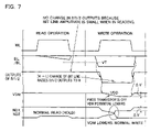
- FIG. 7 represents specific operation waveforms of the memory cell circuit shown in FIG. 4 .
- MOS transistors NQ 3 and NQ 4 shown in FIG. 5 are turned on to couple bit lines BL and /BL to storage nodes ND 1 and ND 2 , respectively.
- the potentials of bit lines BL and /BL change according to the storage data as described above, but the changed levels are higher than the voltage level of input logical thresholds VT of inverters IV 1 and IV 2 .
- the output signals of inverters IV 1 and IV 2 maintain the H level, and both P-channel MOS transistors PT 1 and PT 2 are conductive, so that VDD source line VDM maintains the level of power supply voltage VDD even when it is discharged via the selected memory cell.
- the write data is first transmitted from write driver circuit 5 a shown in FIG. 4 onto bit lines BL and /BL corresponding to the selected column via column select gate CSG (see FIG. 4 ), and these bit lines BL and /BL are set to the H and L levels, respectively.
- bit lines BL and /BL According to the potential changes of bit lines BL and /BL, one of the output signals of inverters IV 1 and IV 2 attains the H level in each of write assist circuits PCKa and PCKb, and corresponding P-channel MOS transistor PT 1 or PT 2 is turned off so that VDD source line VDM enters the floating state.
- word line WL is driven to the selected state, and storage nodes ND 1 and ND 2 are coupled to bit lines BL and /BL, respectively.
- the write data at the logical level opposite to that of the data held in memory cell MC is transmitted so that the through currents flow via MOS transistors PQ 1 , PQ 2 , NQ 1 and NQ 2 .
- the current flows to the bit line at the L level from cell high-side power supply node VH, and the potential of VDD source line VDM in the floating state lowers.
- FIG. 7 represents signal waveforms in such a case that storage nodes ND 1 and ND 2 previously storing the H and L levels data turn to store the L and H level data, respectively.
- the voltage levels of storage nodes ND 1 and ND 2 slowly change depending on the bit line voltages.
- the latching state of the cell is inverted, and the voltage levels of storage nodes ND 1 and ND 2 will rapidly change to the H and L levels depending on the bit line voltages, respectively.
- the potential levels of storage nodes ND 1 and ND 2 change from a stable point to an unstable point without difficulty, and the potentials of these storage nodes ND 1 and ND 2 change to hold the potential levels depending on the write data.
- nodes ND 1 and ND 2 are driven to the levels of voltages (VDD ⁇ V) and VSS according to the write data, the path of the through current is cut off in memory cell MC so that the potential drop of VDD source line VDM stops (i.e., it attains the same voltage level as the high-side storage node when channel resistances of load transistors PQ 1 and PQ 2 are neglected).
- the voltage on the high-side storage node is at the level of the voltage on VDD source line VDM, and MOS transistors PT 1 and PT 2 in each of write assist circuits PCKa and PCKb are in an off state.
- the threshold voltages of the access transistors affect merely to drive the storage node to the voltage level of up to the voltage of (VDD ⁇ Vth) by the write driver if the word line is at the voltage VDD. Therefore, the voltage level of the storage node is lower than voltage VDD.
- bit line WL is driven to the unselected state, and the memory cell stably maintains the data. Then, column select gate CSG isolates bit lines BL and /BL from write driver circuit 5 a , and bit line load circuit 9 (see FIG. 4 ) restores bit lines BL and /BL to the original voltage level.
- both the output signals of inverters IV 1 and IV 2 attain the H level to turn on MOS transistors PT 1 and PT 2 , and the voltage level of VDD source line VDM returns to the level of high-side power supply voltage VDD.
- the voltage on the high side storage node rises to the level of voltage VDD.
- VDD source line VDM of the memory cells on the unselected column and selected row are kept at the level of high-side power supply voltage VDD, and the data holding characteristics of the selected row and unselected columns do not deteriorate so that the possibility of read destruction of the data is extremely low, and the data can be stably held.
- the voltage level of cell high-side power supply node VH lowers, but the access transistors are kept off, so that a path of current flow is not present within each cell, and the storage data is stably held.
- the VDD source line supplying the high-side power supply voltage is selectively maintained in the floating state or the power supplying state according to the bit line potential. In only the data writing operation, therefore, the power supply voltage level of the memory cells in the selected column can be changed, and the write margin can be increased to achieve fast data reading.
- the potential amplitude of the bit line in the selected column is small, the VDD source line is kept at the level of high-side power supply voltage VDD and the memory cell stably holds the data.
- write assist circuits PCKa and PCKb are arranged on the opposite sides of VDD source line VDM, respectively, it is possible to prevent potential lowering that may be caused by the interconnection resistance of VDD source line VDM (the interconnection length of VDD source line can be equivalently reduced to half times), and thereby it is possible to prevent reduction of the static noise margin of the memory cell in the read operation.
- VDD source line is controlled merely based on the bit line potential, and it is not necessary to utilize the column address signal, so that interconnections for using the column address signals for the voltage control are not required.
- the bit line voltage is utilized for setting the state of the VDD source line, the state of the memory cell power supply line is set when a word line is selected, and it is not particularly required to employ a circuit for adjusting timing between setting of the state of the power supply line and the selection of the word line so that the construction for the power supply control can be made simple.
- the write characteristics can be improved, and the memory operation can be stable even when high-side power supply voltage VDD is low. Although there is a lower limit of the voltage level ensuring the data retention characteristics, the power consumption can be reduced by lowering the cell power supply voltage.
- MOS transistors employed in each of write assist circuits PCKa and PCKb for controlling the connection between the VDD source line and the high-side power supply node can be arranged in an optimum position inside the memory cell array, and these may be arranged in a central position of the VDD source line, not only at the opposite sides. Flexibility in layout is improved, and the voltage drop due to the interconnection resistance of the VDD source line can be suppressed so that the operation margin with a low power supply voltage can be maintained.
- FIG. 8 schematically shows a construction of a portion (memory cell circuit) related to memory cells MC in one row of a semiconductor memory device according to a second embodiment of the invention.
- write assist circuits PCKa and PCKb are arranged on the opposite sides of VDD source line VDM.
- VDD source line VDM is individually arranged for each column, and is commonly coupled to high-side power supply nodes VH of memory cells MC arranged in alignment in the corresponding column.
- memory cells MC arranged in four rows are shown as a representative example.
- Word lines WL 0 -WL 3 are arranged corresponding to the respective memory cell rows.
- Bit lines BL and /BL are arranged corresponding to the memory cell column, and bit lines BL and /BL are coupled to an internal data bus IO via column select gate CSG.
- Column select gate CSG is selectively made conductive to couple corresponding bit lines BL and /BL to internal data bus IO according to a column select signal CSL received from a column decoder 4 a .
- Column decoder 4 a is included in the column select circuit shown in FIG. 1 , and decodes column address signal CA received from main control circuit 7 to produce column select signal CSL.
- bit line load circuit is arranged for bit lines BL and /BL, but is not shown in FIG. 8 for the sake of simplicity.
- bit lines BL and /BL are precharged to the H level of power supply voltage VDD.
- This bit line load circuit is kept inactive in the data write operation.
- Write assist circuits PCKa and PCKb have the same construction, and corresponding portions are allotted with the same reference numerals.
- Each of write assist circuits PCKa and PCKb includes a 2-input NAND gate NG 1 receiving the voltages on bit lines BL and /BL, and a P-channel MOS transistor PT 3 for coupling the VDD power supply node to VDD source line VDM according to an output signal of NAND gate NG 1 .
- write assist circuits PCKa and PCKb shown in FIG. 8 differ from those of the first embodiment already described in that 2-input NAND gate NG 1 is employed in place of the inverters arranged for respective bit lines BL and /BL.
- FIG. 9 is a signal waveform diagram representing an operation of the memory cell circuit shown in FIG. 8 .
- the potential of word line WL corresponding to an addressed row rises to the H level (VDD level).
- the access transistors (NQ 3 and NQ 4 ) are turned on to couple storage nodes ND 1 and ND 2 to bit lines BL and /BL in memory cell MC, respectively.
- the potential of the storage node (e.g., ND 2 ) storing L level data rises according to the column current flowing through, e.g., bit line /BL (to attain the voltage level corresponding to the ⁇ -ratio between the transistor (NQ 3 , NQ 4 ) and driver transistor (NQ 1 , NQ 2 ) as well as the resistance value of the bit line load circuit).
- bit lines BL and /BL change according to the storage data of memory cell MC on the selected row.
- Bit lines BL and /BL are coupled to internal data bus IO via column select gate CSG, and the potential level thereof continuously changes.
- the potential amplitudes of bit lines BL and /BL are higher than the voltage level of input logical threshold VTG of NAND gate NG 1 , and NAND gate NG 1 determines that both the voltage levels of bit lines BL and /BL are at the H level, and maintains its output signal at the L level.
- MOS transistor PT 3 maintains the on state, and maintains VDD source line VDM at the level of high-side power supply voltage VDD. Thereby, the data can be read while stably holding the data of memory cell MC, similarly to the first embodiment.
- bit lines BL and /BL are driven to the H and L levels (VDD and VSS levels), respectively, according to the write data supplied from column select gate CSG via write driver circuit 5 a .
- VDD and VSS levels the voltage levels of bit lines BL and /BL are driven to the H and L levels (VDD and VSS levels), respectively, according to the write data supplied from column select gate CSG via write driver circuit 5 a .
- the voltage level of one of bit lines BL and /BL lowers, one of the inputs of NAND gate NG 1 attains the L level, and the output signal thereof attains the H level so that P-channel MOS transistor PT 3 is turned off, and VDD source line VDM enters the floating state.
- storage nodes ND 1 and ND 2 of the memory cell in the selected row are coupled to bit lines BL and /BL, respectively.
- the voltage levels of storage nodes ND 1 and ND 2 in the selected memory cell change.
- word line WL is driven to the unselected state, and bit lines BL and /BL return to the original precharge voltage levels so that NAND gate NG 1 outputs the signal at the L level, and the voltage level of VDD source line VDM returns to the level of high-side power supply voltage VDD.
- NAND gate NG 1 receives the voltages on bit lines BL and /BL to detect the change thereof, and only one P-channel MOS transistor PT 3 is connected between the supply node of high-side power supply voltage VDD and VDD source line VDM. Therefore, the resistance component (channel resistance) between the high-side power supply voltage supplying node and the VDD source line decreases so that the voltage on the VDD source line can rapidly return to high-side power supply voltage VDD. Also, the interconnection resistance of VDD source line VDL is small, and the voltage drop thereof is small so that the cell power supply voltage at the predetermined voltage level (VDD level) can be stably supplied to the high-side power supply node of the memory cell in the corresponding column.
- FIG. 10 schematically shows a construction of a memory cell array of the semiconductor memory device according to a third embodiment of the invention.
- FIG. 10 schematically shows a circuit construction for memory cells MC arranged in four rows and four columns. Bit line pairs BL 0 and /BL 0 , BL 1 and /BL 1 , BL 2 and /BL 2 , and BL 3 and /BL 3 are arranged corresponding to the memory cell columns, respectively.
- Bit lines BL 0 and /BL 0 , and BL 1 and /BL 1 are coupled to a two-to-one selector 4 b 0
- bit lines BL 2 and /BL 2 , and BL 3 and /BL 3 are likewise coupled to a two-to-one selector 4 b 1 .
- These two-to-one selectors 4 b 0 and 4 b 1 perform two-to-one selection according to column address signal CA, and each selects one bit line pair from the corresponding two bit line pairs.
- a write driver 5 a 0 and a sense amplifier circuit 6 a 0 are arranged for two-to-one selector 4 b 0
- a write driver 5 a 1 and a sense amplifier circuit 6 a 1 are arranged for two-to-one selector 4 b 1 .
- These two-to-one selectors 4 b 0 and 4 b 1 are included in column select circuit 4 shown in FIG. 1 , and perform column selecting operations in parallel according to column address signal CA.
- Write driver 5 a 0 and sense amplifier circuit 6 a 0 perform input/output of data DI 0 and DO 0
- write driver 5 a 1 and sense amplifier circuit 6 a 1 perform input/output of data DI 1 and DO 1 . Therefore, the construction shown in FIG. 10 performs write/read of 2-bit data.
- Word lines WL 0 -WL 3 are arranged corresponding to the memory cell row, respectively.
- the memory cells on each bit line pair are divided into a plurality of groups, and a divided VDD source line is arranged for each memory cell group. More specifically, divided VDD source lines VDM 0 A and VDM 0 B are arranged parallel in the column direction for bit lines BL 0 and /BL 0 , and divided VDD source lines VDM 1 A and VDM 1 B are arranged for bit lines BL 1 and /BL 1 .
- Divided VDD source lines VDM 2 A and VDM 2 B are arranged for bit lines BL 2 and /BL 2 , and divided VDD source lines VDM 3 A and VDM 3 B are arranged for bit lines BL 3 and /BL 3 .
- Write assist circuits PCKa 0 -PCKa 3 are arranged corresponding to divided VDD source lines VDM 0 A-VDM 3 A, respectively, and write assist circuits PCKb 0 -PCKb 3 are arranged corresponding to divided VDD source lines VDM 0 B-VDM 3 B, respectively.
- These write assist circuits PCKa 0 -PCKa 3 and PCKb 0 -PCKb 3 have substantially the same constructions as write assist circuits PCKa and PCKb shown in FIG. 8 , and corresponding portions are allotted with the same reference numerals.
- Each of write assist circuits PCKa 0 -PCKa 3 and PCKb 0 -PCKb 3 has an NAND gate NG 1 receiving voltages on the corresponding paired bit lines, and a P-channel MOS transistor PT 3 selectively coupling the supply node of high-side power supply voltage VDD (referred to as a “VDD supply node” hereinafter) to the corresponding divided VDD source line according to the output signal of corresponding NAND gate NG 1 .
- VDD supply node high-side power supply voltage
- NAND gate NG 1 determines that the potentials of the corresponding bit lines are at the H level.
- Each of divided VDD source lines VDM 0 A-VDM 3 A and VDM 0 B-VDM 3 B is kept at the level of high-side power supply voltage VDD, and the data reading is performed stably.
- each of two-to-one selectors 4 b 0 and 4 b 1 performs two-to-one selection to select one bit line pair from the two bit line pairs, and 2-bit data DO 0 and DO 1 are read out.
- two-to-one selectors 4 b 0 and 4 b 1 perform two-to-one selection according to column address signal CA, and write driver circuits 5 a 0 and 5 a 1 drive in parallel the bit lines in the selected columns according to write data bits DI 0 and DI 1 , respectively.
- discharging is performed in the memory cells connected to the selected word line (e.g., word line WL 3 ).
- the potential of the divided VDD source lines corresponding to the selected columns lowers (in the data write operation, all MOS transistors PT 3 in the write assist circuits of the selected columns are already in an off state). It is determined that the bit line potentials of the divided VDD source lines on the unselected columns are at the H level, and associated MOS transistors PT 3 are conductive to hold the corresponding VDD source line at the level of high-side power supply voltage VDD, so that the storage data is stably held.
- All the memory cells corresponding to divided VDD source lines VDM 0 A-VDM 3 A provided for the unselected word lines are unselected, and divided VDD source lines VDM 0 A-VDM 3 A are in the floating state. However, a path of current flow from the high-side power supply node to the low-side power supply node is not present in these memory cells, and divided VDD source lines VDM 0 A-VDM 3 A maintain the level of power supply voltage VDD.
- bit lines BL 1 and /BL 1 are unselected, and the bit line load circuit (not shown) causes current to flow through the corresponding memory cell MC to lower the voltage level of one of bit lines BL 1 and /BL 1 from the precharged voltage level.
- the amount of this potential drop is similar to that in the data read operation.
- write assist circuit PCKb 1 the output signal of NAND gate NG 1 is at the L level, and MOS transistor PT 3 is conductive, so that high-side power supply voltage VDD is stably supplied to the memory cells to hold stably the data.
- the VDD source line provided corresponding to each memory cell column is divided, and the voltage level of each divided VDD source line is controlled according to the potential of the corresponding bit line so that the interconnection capacitance of the VDD source line is reduced, and the potential of the divided VDD source line lowers rapidly in the data write operation. Therefore, fast writing can be performed. After the end of the writing, the potential of the divided VDD source line in the selected column can be rapidly restored to the level of power supply voltage VDD, and the write time can be reduced.
- the influence of the interconnection resistance of the divided VDD source line is similar to that in the case where one continuous VDD source line is arranged for each column, and write assist circuits are arranged on the opposite ends thereof, as in the first embodiment.
- the memory cell array has the VDD source lines each divided into two, and write assist circuits PCKa 0 -PCKa 3 are arranged in boundary regions of the divided VDD source lines.
- write assist circuits PCKa 0 -PCKa 3 are arranged on the other ends (near the two-to-one selector) of divided VDD source lines VDM 0 A-VDM 3 A, and write assist circuits PCKa 0 -PCKa 3 and PCKb 0 -PCKb 3 are arranged opposingly on the opposite ends of the memory cell array.
- VDD source line in each column is divided into two, it may be divided into more than two lines.
- the interconnection length thereof can be short, and accordingly, the interconnection capacitance can be reduced so that the voltage change can be performed fast, and the write operation can be performed fast.
- the memory cells in two columns are arranged for each data bit, the number of memory cell columns arranged per data bit is not restricted to two, and can be appropriately determined.
- the data to be input/output concurrently may have a larger bit width than the above, and may have a width, e.g., of 8 or 16 bits.
- FIG. 11 shows a construction of a write assist circuit according to a fourth embodiment of the invention.
- FIG. 11 representatively shows a construction of a write assist circuit PCK provided for one bit line pair BL and /BL.
- Arrangements in the memory cell array can be any of the constructions in the first to third embodiments already described.
- Write assist circuit PCK includes a power supply control section VCT for controlling the impedance of VDD source line VDM according to the voltage levels of bit lines BL and /BL, a one-shot pulse producing circuit 10 for producing a pulse signal of one shot according to a bit line voltage detection signal applied from power supply control section VCT, and an N-channel MOS transistor NT 1 for driving VDD source line VDM to the low-side power supply voltage (VSS: second power supply voltage) level according to the output signal of one-shot pulse producing circuit 10 .
- VCT power supply control section
- VCT for controlling the impedance of VDD source line VDM according to the voltage levels of bit lines BL and /BL
- a one-shot pulse producing circuit 10 for producing a pulse signal of one shot according to a bit line voltage detection signal applied from power supply control section VCT
- an N-channel MOS transistor NT 1 for driving VDD source line VDM to the low-side power supply voltage (VSS: second power supply voltage) level according to the output signal of one-shot pulse
- Power supply control section VCT includes NAND gate NG 1 receiving voltages on bit lines BL and /BL, and P-channel MOS transistor PT 3 coupling the VDD supply node to VDD source line VDM according to the output signal of NAND gate NG 1 . Therefore, power supply control section VCT corresponds to the construction of the write assist circuits of the foregoing second and third embodiments, and has a similar construction.
- One-shot pulse producing circuit 10 includes an inversion delay circuit 11 that inverts and delays by a predetermined time the output signal of NAND gate NG 1 , and an AND gate AG 1 receiving the output signal of inversion delay circuit 11 and the output signal of NAND gate NG 1 .
- One-shot pulse producing circuit 10 produces a one-shot pulse signal having a predetermined time width in response to rising of the output signal of NAND gate NG 1 .
- the H level time period of the one-shot pulse signal is determined by the delay time of inversion delay circuit 11 .
- FIG. 12 is a signal waveform diagram representing an operation for data writing of write assist circuit PCK shown in FIG. 11 . Referring to FIG. 12 , description will now be given of an operation of write assist circuit PCK shown in FIG. 11 .
- one-shot pulse producing circuit 10 produces a pulse signal of one shot that is kept at H level for a predetermined period of time.
- MOS transistor PT 3 is turned off to isolate VDD source line VDM from the VDD supply node.
- MOS transistor NT 1 is turned on.
- VDD source line VDM isolated from the VDD supply node is coupled to the low-side power supply node to lower the voltage level thereof.
- the data holding characteristics of the storage nodes (ND 1 and ND 2 : not shown) rapidly lower according to the potential drop of VDD source line VDM, and potential levels thereof rapidly change according to the potential levels of bit lines BL and /BL.
- the time required for the data writing (the time required for setting storage nodes ND 1 and ND 2 to the potential levels corresponding to the write data) can be reduced, and fast writing is achieved.
- word line WL is driven to the unselected state, and the column select circuit isolates bit lines BL and /BL from the internal data lines.
- the bit line load circuit (not shown) restores the voltage levels of bit lines BL and /BL to the original level of the precharge voltage.
- the one-shot pulse signal produced from one-shot pulse producing circuit 10 is already at the L level, and MOS transistor NT 1 is in an off state.
- the output signal of NAND gate NG 1 in power supply control section VCT attains the L level so that MOS transistor PT 3 returns VDD source line VDM to the original voltage level (VDD level).
- the voltage level of the VDD source line is driven toward the level of low-side power supply voltage VSS in response to the change in bit line potential for a predetermined period time, and the voltage level thereof is forcedly lowered. This can increase the write margin of the memory cell, and can achieve the fast writing.
- the unselected memory cells can stably hold the data even in the data write mode, similarly to the first to third embodiments.
- FIG. 13 shows a construction of write assist circuit PCK according to a fifth embodiment of the invention.
- Voltage control circuit PCK shown in FIG. 13 includes a P-channel MOS transistor PT 4 for driving VDD source line VDM to the second power supply voltage (low-side power supply voltage VSS) level when the potentials of bit lines BL and /BL change.
- One-shot pulse producing circuit 10 controls the on/off state of MOS transistor PT 4 .
- One-shot pulse producing circuit 10 produces a pulse signal of one shot that is kept at L level for a predetermined time period in response to the rising of the output signal of NAND gate NG 1 included in power supply control section VCT, and provides the pulse signal to the gate of P-channel MOS transistor PT 4 .
- Power supply control section VCT has the same construction as power supply control section VCT shown in FIG. 11 . Corresponding portions are allotted with the same reference numerals, and description thereof is not repeated.
- One-shot pulse producing circuit 10 includes inversion delay circuit 11 , and an NAND gate NG 2 receiving the output signal of inversion delay circuit 11 and the output signal of NAND gate NG 1 of power supply control section VCT.
- the L level time period of the one-shot pulse signal produced by one-shot pulse producing circuit 10 is determined by the delay time of inversion delay circuit 11 .
- FIG. 14 is a signal waveform diagram representing an operation for data writing of write assist circuit PCK shown in FIG. 13 . Referring to FIG. 14 , description will now be given of the operation of write assist circuit PCK shown in FIG. 13 .
- the voltage levels of bit lines BL and /BL corresponding to the selected column are driven to the H and L levels according to the write data, respectively.
- the signal applied from power supply control section VCT to node NDA rises to the H level, and responsively, the one-shot pulse signal applied from one-shot pulse producing circuit 10 to a node NDC is kept at the L level for a predetermined time period.
- MOS transistor PT 4 is turned on to drive VDD source line VDM toward the low-side power supply voltage.
- MOS transistor PT 3 is kept off by the output signal of NAND gate NG 1 , and VDD source line VDM isolated from the VDD supply node has the voltage level rapidly lowered. Therefore, the write margin increases similarly to the construction of the write assist circuit of the fourth embodiment shown in FIG. 11 , and the potential levels of the storage nodes (ND 1 and ND 2 ) of the selected memory cell can be rapidly changed according to the write data.
- bit lines BL and /BL are in the unselected column, or are in the data read mode, the potentials of bit lines BL and /BL are at the H level, the output signal of NAND gate NG 1 is at the L level and MOS transistor PT 3 is in an on state. Since the output signal of NAND gate NG 1 is fixed at the L level, output node NDC of one-shot pulse producing circuit 10 maintains the H level, and MOS transistor PT 4 maintains the off state. Therefore, the bit lines on the unselected columns and the bit lines in the data read operation are in such a state that VDD source line VDM is reliably supplied with high-side power supply voltage VDD, the static noise margin is ensured and the data is stably held.
- FIG. 15 schematically shows sectional structures of MOS transistors PT 3 and PT 4 shown in FIG. 13 .
- MOS transistors PT 3 and PT 4 are formed in an N-well 20 .
- P-channel MOS transistor PT 3 includes P-type impurity regions 21 c and 21 d formed at the surface of N-well 20 with a space between them, and a gate electrode 22 b formed on a well region surface between impurity regions 21 c and 21 d with a gate insulating film (not shown) interposed in between.
- P-channel MOS transistor PT 4 includes P-type impurity regions 21 a and 21 b formed separately and distantly at the surface of N-well 20 , and a gate electrode 22 a formed on a well region surface between impurity regions 21 a and 21 b with a gate insulating film interposed in between.
- Impurity region 21 a is coupled to receive low-side power supply voltage VSS, and impurity region 21 d is coupled to receive high-side power supply voltage VDD.
- Gate electrodes 22 a and 22 b are coupled to nodes NDC and NDA shown in FIG. 13 , respectively.
- Impurity regions 21 b and 21 c are coupled to VDD source line VDM.
- N-well 20 is biased to the level of high-side power supply voltage VDD.
- Impurity regions 21 b and 21 c may be formed continuously to each other, or an element isolating region may be formed in between.
- MOS transistor PT 3 When node NDA is at the H level of voltage VDD, MOS transistor PT 3 is in an off state and isolates the VDD supply node from VDD source line VDM. When node NDC is at the L level, a channel is formed between impurity regions 21 a and 21 c , and VDD source line VDM is coupled to low-side power supply voltage VSS.
- VDD source line VDM excessively lowers to deteriorate the data retention characteristics of the unselected memory cells, and to destroy the data held in the memory cells on the selected column and unselected row.
- the P-channel MOS transistor is used for the VDD source line to lower forcedly the potential level of the VDD source line in the floating state when the bit line potential changes. Accordingly, the voltage level of the VDD source line in the selected column lowers fast, the excessive lowering of the voltage level can be prevented, and it is possible to prevent destruction of the data held in the memory cells on the selected column and unselected rows. Also, excessive lowering of the VDD source line voltage can be prevented so that the VDD source line can rapidly return to the original voltage level after the completion of the write operation.
- FIG. 16 shows a construction of write assist circuit PCK according to a sixth embodiment of the invention.
- a diode-connected P-channel MOS transistor PT 5 is connected to VDD source line VDM.
- Diode-connected P-channel MOS transistor PT 5 has a gate and a drain connected to VDD source line VDM, and has a source coupled to a VDD supply node.
- Power supply control section VCT has the same construction as the write assist circuits of the first to fifth embodiments, and includes NAND gate NG 1 receiving the voltages on bit lines BL and /BL as well as P-channel MOS transistor PT 3 selectively isolating VDD source line VDM from the VDD supply node according to the output signal of NAND gate NG 1 .
- FIG. 17 is a signal waveform diagram representing an operation for data writing of write assist circuit PCK shown in FIG. 16 . Referring to FIG. 17 , description will now be given of operations of write assist circuit PCK shown in FIG. 16 .
- the voltage levels of bit lines BL and /BL in the selected column change to H and L levels according to the write data.
- the output signal of NAND gate NG 1 attains the H level to turn off MOS transistor PT 3 .
- MOS transistor PT 5 is turned off when VDD source line VDM is at the level of voltage equal to or higher than (VDD ⁇ Vtp), where Vtp is an absolute value of the threshold voltage of MOS transistor PT 5 .
- VDD source line VDM When VDD source line VDM is at the level of voltage lower than (VDD ⁇ Vtp), MOS transistor PT 5 is turned on to couple VDD source line VDM to the VDD supply node, and prevents the potential lowering of VDD source line VDM. Therefore, the voltage level of VDD source line VDM is clamped at the level of (VDD ⁇ Vtp).
- clamp transistor PT 5 can prevent excessive drop of the voltage level of VDD source line VDM in the selected column, and can suppress deterioration of the data holding characteristics of the memory cells on the selected column and unselected rows, so that the destruction of the held data can be prevented.
- the voltage level clamping element for VDD source line VDM may be formed of another element such as a PN-diode.
- voltage clamp means is employed for suppressing the lowering of the voltage level of the VDD source line, and it is possible to prevent destruction of the data held in the memory cells on the selected column and unselected row (because excessive lowering of the high-side power supply voltage can be prevented and accordingly, the lowering of the data holding characteristics can be suppressed).
- FIG. 18 shows a construction of write assist circuit PCK according to a seventh embodiment of the invention.
- Write assist circuit PCK shown in FIG. 18 differs in the following constructions from the write assist circuit shown in FIG. 16 .
- Power supply control section VCT includes an NAND gate NG 3 receiving a redundant signal CRD and the voltages on bit lines BL and /BL in place of NAND gate NG 1 receiving the voltages on bit lines BL and /BL.
- MOS transistor PT 3 selectively couples the VDD supply node to VDD source line VDM according to the output signal of this NAND gate NG 3 .
- Redundant signal CRD designates a defective column in the memory cell array.
- the bit lines in the faulty or defective column are normally kept in the unselected state, and the address of the defective column is replaced by a spare bit line pair.
- By replacing the bit lines on the faulty column with the spare bit line pair it becomes possible to use the address of the faulty column to repair the faulty column.
- a P-channel MOS transistor PT 6 that is selectively turned on in accordance with the output signal of inverter IV 3 is connected between diode-connected P-channel MOS transistor PT 5 and the VDD supply node. Inverter IV 3 receives redundant signal CRD.
- VDD source lines VDM are arranged corresponding to the memory cell columns for controlling the voltage levels of the columns, respectively, and further the power supplying is controlled for the faulty column in the faulty column repairing.
- redundant signal CRD for the faulty column is set to the L level
- the output signal of NAND gate NG 3 is fixed at the H level so that MOS transistor PT 3 is normally set in the off state.
- the output signal of inverter IV 3 is at the H level, and the MOS transistor PT 6 is normally in an off state so that the current path between the VDD supply node and MOS transistor PT 5 is cut off.
- VDD source line VDM is completely isolated from the VDD supply node, and a path of a leakage current due to the faulty memory cell on the faulty column is cut off so that the power consumption is made small.
- redundant signal CRD is set to the H level.
- the logical level of output signal of NAND gate NG 3 depends on the potentials of bit lines BL and /BL, the output signal of inverter IV 3 is fixed at the L level, and MOS transistor PT 6 is turned on. In this case, therefore, operations similar to those of write assist circuit PCK shown in FIG. 16 is implemented.
- FIG. 19 schematically shows a construction of a main portion of a semiconductor memory device according to a seventh embodiment of the invention.
- a memory cell array includes a normal memory cell array 1 n having normal memory cells MC arranged in rows and columns, and a spare memory cell array 1 s having spare memory cells SMC for repairing a faulty column.
- the faulty column may be repaired in a so-called shift redundancy manner, in which the correspondence between the bit lines and the column decoder outputs is shifted except the faulty column.
- FIG. 19 shows a construction of repairing the faulty column by merely replacing the faulty column in normal memory cell array with the spare bit line pair.
- bit line pairs BLP For normal memory cell array in, there is provided bit line pairs BLP, VDD source lines VDM corresponding to respective bit line pairs BLP and write assist circuits PCK corresponding to respective VDD source lines VDM.
- a spare bit line pair SBLP is arranged corresponding to spare memory cell column SMC, and a spare VDD source line SVDM is arranged corresponding to spare bit line pair SBLP.
- the number of spare bit line pairs SBLP in spare memory cell array 1 s is determined depending on the number of faulty columns to be repaired.
- the column select circuit includes a regular column select circuit 4 n arranged for regular memory cell array 1 n , and a redundant column select circuit 4 s arranged corresponding to memory cell array 1 s.
- a redundant column replacement control circuit 20 is arranged for controlling the operations of normal and redundant column select circuits 4 n and 4 s .
- Redundant column replacement control circuit 20 includes a program circuit storing a faulty column address specifying a faulty column, and produces a normal column select enable signal NE and a spare column select enable signal NEZ according to coincidence/non-coincidence between column address signal CA and the programmed faulty column address.
- redundant column replacement control circuit 20 When the selected column in the designated address is non-defective, redundant column replacement control circuit 20 activates normal selection enable signal NE, and normal column select circuit 4 n selects bit line pair BLP corresponding to the column in the designated address. Redundant column select circuit 4 s is inactive, and the spare column is kept in the unselected state.
- column address signal CA designates the faulty column
- redundant column replacement control circuit 20 activates faulty spare column replacement enable signal NEZ, and redundant column select circuit 4 s selects corresponding spare bit line pair SBLP employed for the redundancy replacement. In this case, normal column select circuit 4 n stops the column select operation (signal NE is inactive).
- a cell power supply control unit 22 for controlling enabling/disabling of each of write assist circuits PCK on a column-by-column basis.
- Cell power supply control unit 22 operates according to faulty column information to produce redundant signal CRD for corresponding write assist circuit PCK.
- FIG. 20 shows an example of a construction of a circuit producing the redundant signal for the VDD source line in one column included in power supply control unit 22 shown in FIG. 19 .
- the redundant signal producing unit includes a link element FL which is connected between the high-side power supply node and an internal node ND 10 , and can be blown, a highly resistive resistance element Z having an end connected to internal node ND 10 , an inverter IV 10 inverting a voltage signal on internal node ND 10 , an inverter IV 11 inverting the output signal of inverter IV 10 to produce redundant signal CRD, an N-channel MOS transistor NT 10 which is connected between highly resistive resistance element Z and the low-side power supply node, and has a gate receiving the output signal of inverter IV 10 , and an N-channel MOS transistor NT 11 which is connected between highly resistive resistance element Z and the low-side power supply node, and has a gate receiving a reset signal RST.
- reset signal RST Upon system resetting or system power up, reset signal RST attains H level and is kept at H level for a predetermined time period. Link element FL for the faulty column is blown off.
- node ND When link element FL is blown, node ND is isolated from the high-side power supply node (VDD).
- MOS transistor NT 11 When MOS transistor NT 11 is turned on according to reset signal RST, internal node ND 10 is driven to the voltage level of the low-side power supply node through highly resistive resistance element Z. Thereby, the output signal of inverter IV 10 attains the H level to turn on MOS transistor NT 10 . Even when reset signal RST attains the L level to turn off MOS transistor NT 11 , node ND 10 is maintained at the level of the voltage on the low-side power supply node by highly resistive resistance element Z and MOS transistor NT 10 . In this state, inverter IV 11 fixes redundant signal CRD at the L level to stop the control of power supplying of the VDD source line to the faulty column, and the corresponding VDD source line is normally kept in the floating state.
- the power supply control unit 22 As the construction of cell power supply unit 22 , the power supply control unit is shown as replacing a faulty column with the spare column. However, the faulty column may be repaired according to the shift redundancy scheme. For repairing the faulty column in the shift redundancy scheme, a propagation path to the column select gate of the column select signal applied from the column decoder is switched. Cell power supply control unit 22 may produce redundant signal CRD by using a signal for instructing such path switching. Specifically, where there are two propagation paths for a column select gate of each column select signal, and one of the signal propagation paths is to be used, the paths are switched such that the column select signal is not propagated to the column select gate for the faulty column.
- the propagation path of the column select signal is switched in the faulty column, the signal setting the column select signal propagation path for the adjacent column differs in logical level from the signal setting the propagation path of the column select signal for the faulty column. Therefore, the redundant signal can be produced for each column by utilizing, in each column, a gate circuit for determining whether the signals of setting the propagation paths of the column select signals in a pair of adjacent columns are the same in logic level.
- the power supply control is stopped on the VDD source line for the faulty column, and the corresponding VDD source line is forced into the floating state.
- the leakage current due to a memory cell in the faulty column can be prevented from flowing, and therefore the current consumption can be reduced.
- FIG. 21 shows a construction of write assist circuit PCK according to an eighth embodiment of the invention.
- Write assist circuit PCK shown in FIG. 21 includes an inverter IV 13 receiving the output signal of NAND gate NG 1 of power supply control section VCT, and a P-channel MOS transistor PT 13 coupling VDD source line VDM to an intermediate voltage supply node according to an output signal of inverter IV 13 .
- Power supply control section VCT includes NAND gate NG 1 and P-channel MOS transistor PT 3 , similarly to the first to seventh embodiments already described.
- MOS transistor PT 3 is coupled to the node (VDD supply node) receiving an ordinary power supply voltage VDD 1 .
- MOS transistor PT 13 is coupled to an intermediate voltage node receiving a voltage VDD 2 lower than this ordinary power supply voltage VDD 1 .
- FIG. 22 is a signal waveform diagram representing an operation for writing of write assist circuit PCK shown in FIG. 21 . Referring to FIG. 22 , description will now be given of the operations for data writing of write assist circuit PCK shown in FIG. 21 .
- bit lines BL and /BL are supplied with the voltages corresponding to the write data, and the voltages on these bit lines are driven to the H and L levels.
- the output signal of NAND gate NG 1 attains the H level
- MOS transistor PT 3 is turned off to isolate VDD source line VDM from the node supplying voltage VDD 1 .
- the output signal of inverter IV 13 attains the L level to turn on MOS transistor PT 13
- VDD source line VDM receives intermediate voltage VDD 2 .
- This voltage VDD 2 is lower than the voltage VDD 1 at the ordinary power supply voltage level.
- the voltage level of VDD source line VDM is reliably lowered, the write margin of the memory cell can be reliably increased and the data can be written fast.
- the voltage VDD 2 is generated from the circuit for producing intermediate voltage VDD 2 , and VDD source line VDM can be set to a desired voltage level without receiving an influence of variations in threshold voltage caused due to transistor parameters, as in the construction of using a diode-connected MOS transistor.
- VDD source line VDM can be set to a desired voltage level without receiving an influence of variations in threshold voltage caused due to transistor parameters, as in the construction of using a diode-connected MOS transistor.
- FIG. 23 schematically shows a construction of a power supply voltage generating section for generating two voltages VDD 1 and VDD 2 shown in FIG. 21 .
- the power supply voltage generating section includes a power supply circuit 25 that receives externally supplied power supply voltage VDD, and effects stabilization processing such as noise removal on it to produce cell power supply voltage VDD 1 , and a voltage down converter 26 for down-converting an output voltage VDD 1 of power supply circuit 25 to produce intermediate voltage VDD 2 .
- Power supply circuit 25 simply performs the filtering processing such as noise removal, to produce cell power supply voltage VDD 1 at the same voltage level as the externally supplied power supply voltage VDD.
- intermediate voltage VDD 2 may be produced with a circuit construction for converting an output current of a reference current generating circuit to a voltage.
- VDC feedback controlled internal voltage down converter
- DRAM Dynamic Random Access Memory
- cell power supply voltage VDD 1 and intermediate voltage VDD 2 stably at desired voltage levels can be produced from externally supplied power supply voltage VDD.
- the VDD source line voltage is switched, according to the bit line voltage, between ordinary power supply voltage VDD 1 and the lower intermediate voltage VDD 2 , and the VDD source line voltage for a selected column can be reliably set at a desired voltage level in the data writing, so that the data can be written stably and fast.
- the VDD source line voltage in the selected column can be set to a desired voltage level, and it is possible to prevent deterioration of the data holding characteristics of unselected memory cells and to prevent destruction of the data held in the unselected memory cells.
- FIG. 24 shows a construction of a main portion of a semiconductor memory device according to a ninth embodiment of the invention.
- FIG. 24 shows a construction of a write assist circuit for memory cells MC aligned in one column.
- Memory cells MC are arranged in four rows and one column, and word lines WL 0 -WL 3 are arranged corresponding to the respective rows.
- Bit lines BL and /BL are arranged corresponding to the memory cell column.
- VDD source line VDM is arranged, similarly to the first to eighth embodiments.
- a dummy VSS source line DVSM is arranged extending in parallel to VDD source line VDM and corresponding to each memory cell column.
- a VSS source line supplying low-side power supply voltage VSS to the memory cells are also arranged separately from the dummy source lines, although not shown in the figure.
- Write assist circuits PCKa and PCKb are arranged opposingly at the opposite ends of VDD source line VDM and dummy VSS source line DVSM, precharge dummy VSS source line DVSM and adjust the voltage level of VDD source line by coupling selectively VDD source line VDM and dummy VSS source line DVSM to utilize accumulated charges on the dummy VSS source line.
- Each of write assist circuits PCKa and PCKb has the same construction, and corresponding portions are allotted with the same reference numerals.
- Each of write assist circuits PCKa and PCKb includes power supply control section VCT for isolating VDD source line VDM from the VDD supply node according to the change in voltage levels of bit lines BL and /BL, an inverter IV 15 for inverting the output signal of NAND gate NG 1 included in power supply control section VCT, a transmission gate TX for selectively connecting VDD source line VDM to dummy VSS source line DVSM according to the output signals of NAND gate NG 1 and inverter IV 15 , and an N-channel MOS transistor NT 15 for coupling dummy VSS source line DVSM to the low-side power supply node (VSS supply node) according to an output signal of inverter IV 15 .
- Transmission gate TX is configured of a CMOS transmission gate formed of a parallel connection of P- and N-channel MOS transistors, and transmits a voltage signal without causing a loss of threshold voltage.
- FIG. 25 is a signal waveform diagram representing an operation in data writing of the write assist circuit shown in FIG. 24 . Referring to FIG. 25 , description will now be given of operations of write assist circuits PCKa and PCKb shown in FIG. 24 .
- VDD source line VDM is maintained at the level of high-side power supply voltage VDD
- dummy VSS source line DVSM is maintained at the level of the low-side power supply voltage (VSS).
- bit lines BL and /BL When the data writing starts and the write data is transmitted to bit lines BL and /BL on the selected column, the voltage levels on bit lines BL and /BL change according to the write data. According to the potential changes of bit lines BL and /BL, the output signal of NAND gate NG 1 (voltage on node NDA) attains the H level in power supply control section VCT. Responsively, MOS transistors PT 3 and NT 15 are turned off. In contrast, transmission gate TX is turned on to electrically couple VDD source line VDM to dummy VSS source line DVSM. These VDD source line VDM and dummy VSS source line DVSM are in the floating state, and accumulated charges move between dummy VSS source line DVSM and VDD source line VDM.
- VDD source line VDM has a capacitance of Cd
- dummy VSS source line DVSM has a capacitance of Cs
- the capacitance ratio (Cd:Cs) is 10:1
- the potential of VDD source line is at the level increased by 10/11 times through equalizing by transmission gate TX, and thus lowers by about 10%.
- the voltage level of high-side power supply node lowers to increase the write margin for a selected memory cell MC, so that the storage data of the memory cell can be readily inverted, the write time can be reduced and the writing can be reliably performed.
- the voltage level of the storage node changes to the extent, at most, similar to that in the read operation, and the storage data can be stably held.
- the voltage level of VDD source line VDM lowers more rapidly than the case where the voltage level of the VDD source line lowers through discharging by writing into the memory cell, and the faster write can be achieved.
- bit line load circuit (not shown) returns bit lines BL and /BL to the original H level of voltage VDD after the completion of writing, the output signal of NAND gate NG 1 attains the L level, and responsively, transmission gate TX turns non-conductive, so that MOS transistors PT 3 and NT 15 are turned on. Accordingly, VDD source line VDM and dummy VSS source line DVSM return to the levels of high-side power supply voltage VDD and low-side power supply voltage VSS, respectively.
- This dummy VSS source line DVSM is laid at the same or different interconnection layer that is the same as or different from VDD source line VDM, using an interconnection line extending over memory cells MC.
- VDD source line VDM and dummy VSS source line DVSM can be arranged in each column.
- VDD source line VDM ad dummy VSS source line DVSM can have the same interconnection length even when the rows of memory cells increase in number. Thereby, the capacitance ratio of Cusecs can be kept constant.
- the rows and/or columns in the memory cell array change in number, it is merely required to extend VDD source line VDM and dummy VSS source line DVSM linearly in the column direction, and it is not necessary to redesign the interconnection layout.
- the write assist circuits of the same layout can be utilized, and it is possible to suppress increase in area of the cell power supply control unit when the memory cell array configuration changes (only the number of the write assist circuits is changed according to the number of columns, and it is not necessary to change the configuration of the write assist circuit even when the number of the memory cells in the column direction changes).
- high-side power supply node VH of memory cell MC is connected to VDD source line VDM, and a parasitic capacitance thereof is present.
- the capacitance ratio between VDD source line VDM and dummy VSS source line DVSM is determined taking the parasitic capacitance of high-side power supply node VH into account.
- the dummy VSS source line and VSS source line are set to the floating state according to the bit line voltage and are electrically short-circuited in the data write operation, so that it is possible to lower rapidly the voltage level of VDD source line and to increase the write margin of the selected memory cell, and accordingly, the data can be written fast.
- FIG. 26 shows a construction of a memory cell circuit according to a tenth embodiment of the invention.
- FIG. 26 shows a construction of the write assist circuit for the memory cells arranged in one column.
- memory cells MC are arranged in four rows and one column, and word lines WL 0 -WL 3 are arranged corresponding to the respective rows.
- Bit lines BL and /BL are arranged corresponding to each memory cell column, and are coupled to column select gate CSG and bit line load circuit 9 .
- the construction described above is the same as those of the first to ninth embodiments already described, and is substantially the same in arrangement as the conventional memory cell array.
- VSS source line VSM transmitting low-side power supply voltage VSS is arranged corresponding to the memory cell column.
- VSS source lines VSM are used as cell power supply lines PVL 0 -PVLn.
- the voltage level (impedance) of VSS source line VSM is controlled according to the voltage levels of bit lines BL and /BL in the corresponding column.
- Write assist circuits PCKc and PCKd are arranged on the opposite ends of VSS source line VSM.
- Write assist circuits PCKc and PCKd have the same construction, and each include N-channel MOS transistors NT 20 and NT 21 connected in series between the low-side power supply node and VSS source line VSM. Gates of MOS transistors NT 20 and NT 21 are connected to bit lines BL and /BL on the corresponding column, respectively.
- VSS source line VSM is arranged in an isolated manner for each column.
- FIG. 27 schematically shows internal connections of memory cell MC shown in FIG. 26 .
- the source-side nodes of driver transistors NQ 1 and NQ 2 , or low-side power supply nodes VL are commonly coupled to VSS source line VSM.
- the source nodes of load transistors PQ 1 and PQ 2 , or high-side power supply nodes VH are normally supplied with power supply voltage VDD.
- Storage nodes ND 1 and ND 2 are coupled to bit lines BL and /BL via access transistors NQ 3 and NQ 4 , respectively.
- FIG. 28 is a signal waveform diagram representing an operation of the memory cell circuit shown in FIG. 26 . Referring to FIG. 28 , description will now be given of the operation of the memory cell circuit shown in FIGS. 26 and 27 .
- word line WL is driven to the selected state, and access transistors NQ 3 and NQ 4 in memory cell MC are turned on. Accordingly, storage nodes ND 1 and ND 2 are coupled to bit lines BL and /BL, respectively, and the potential levels of bit lines BL and /BL change according to the data held at storage nodes ND 1 and ND 2 . In this operation, however, the potential changes of bit lines BL and /BL are small owing to the column current supplied from bit line load circuit 9 , and the voltage levels of bit lines BL and /BL are sufficiently higher than threshold voltage Vth of MOS transistors NT 20 and NT 21 .
- both MOS transistors NT 20 and NT 21 are conductive, and VSS source line VSM is coupled to the low-side power supply node, and is stably maintained at the level of low-side power supply voltage VSS. Therefore, even when the voltage levels of storage nodes ND 1 and ND 2 rise according to the column current, the noise margin is sufficiently large, and memory cell MC stably holds the data.
- low-side power supply voltage VSM is stably maintained at the level of low-side power supply voltage VSS, and high-side power supply node VH is coupled to high-side power supply voltage VDD so that the static noise margin is sufficiently ensured, and the storage data is stably held.
- the voltage levels of bit lines BL and /BL change according to the write data.
- MOS transistor NT 20 or NT 21 is turned off, so that VSS source line VSM is isolated from the low-side power supply node and enters the floating state. It is now assumed that the data at the logical level opposite to that of the storage data is written in the data writing operation.
- VSS source line VSM When the voltage level of VSS source line VSM rises, the write margin of memory cell MC increases, and the voltage levels of storage nodes ND 1 and ND 2 rapidly changes according to the write data on bit lines BL and /BL so that the data can be written correctly.
- column select gate CSG isolates bit lines BL and /BL from the internal data line, and bit line load circuit 9 drives them to the level of high-side power supply voltage VDD.
- MOS transistor NT 20 or NT 21 changes from the off state to the on state, and couples VSS source line VSM to the low-side power supply node, and the voltage level thereof returns to the level of low-side power supply voltage VSS.
- bit lines BL and /BL are coupled to storage nodes ND 1 and ND 2 , respectively.
- the write data is not transmitted to the associated bit lines, and bit lines BL and /BL are held at the voltage level precharged by bit line load circuit 9 so that only a minute potential change similar to that in the data reading occurs on the corresponding bit lines, and each memory cell on the unselected column and the selected row stably holds the storage data (because the low-side power supply voltage of VSS source line VSM is maintained at the VSS level).
- the data holding characteristics of the selected memory cell in the write operation can be lowered to perform fast writing even in such a construction that the VSS source line is used as memory cell power supply line PVL, and low-side cell power supply voltage VSS is controlled according to the bit line voltage during the data write operation.
- FIG. 29 shows a construction of a memory cell circuit according to an eleventh embodiment of the invention.
- the memory cell circuit shown in FIG. 29 differs from the memory cell circuit shown in FIG. 26 in the following constructions.
- an AND gate AG 10 receiving the voltages on bit lines BL and /BL
- an N-channel MOS transistor NT 22 receiving the output signal of AND gate AG 10 .
- MOS transistor NT 22 is coupled between the low-side power supply node and VSS source line VSM, and is made conductive to couple the low-side power supply node to VSS source line VSM.
- FIG. 29 Other constructions of the memory cell circuit shown in FIG. 29 are the same as those of the memory cell circuit shown in FIG. 26 . Corresponding portions are allotted with the same reference numerals, and description thereof is not repeated.
- the memory cell construction shown in FIG. 29 operates substantially in the same manner as the memory cell circuit of the tenth embodiment.
- the output signal of AND gate AG 10 attains the L level, and thereby MOS transistor NT 22 is turned off.
- VSS source line VSM enters the floating state, and the voltage level thereof rises due to the write current and through current in the selected memory cell, so that the write margin of the selected memory cell increases, and fast writing is achieved.
- bit lines BL and /BL have the voltage levels lower only slightly than the level of voltage that is precharged by bit line load circuit 9 , and higher than the input logical threshold of AND gate AG 10 , so that the memory cell stably holds the storage data.
- the storage nodes (ND 1 and ND 2 ) are isolated from the corresponding bit lines BL and /BL, and a path of current flow does not exist, so that the voltage levels of the storage nodes are stably maintained.
- the construction shown in FIG. 29 achieve fast data writing without destroying the storage data of unselected memory cells, and can stably hold the held data in reading the held data, as is done in the preceding embodiments already described.
- VSS source line VSM may likewise be divided into portions each corresponding to a predetermined number of rows of memory cells in the memory cell column, and the write assist circuit may be arranged for each divided line.
- the AND gate receives the bit line voltage, and the corresponding VSS source line is selectively coupled to the low-side power supply node according to the output signal of that AND gate. Therefore, the stable reading and fast writing of the data of memory cell can be achieved.
- the interconnection resistance of the VSS source line is equivalently reduced so that the fast reading can be performed.
- the constructions can be utilized, such as the foregoing construction of controlling the voltage level of the VDD source line, the construction of clamping or maintaining it at a specific power supply voltage, the construction of coupling it to another voltage supply.
- a clamping element formed of diode-connected MOS transistor may be arranged between the VSS source line and the ground node, and thereby it is possible to suppress the rising of the voltage level of VSS source line VSM to the level equal to or higher than the threshold voltage of the diode-connected MOS transistor.
- a dummy VDD source line may be used and coupled selectively to the VSS source line in the data write operation, whereby the voltage level of the VSS source line can be raised.
- the VSS source line may be coupled to the power supply node that supplies a predetermined intermediate voltage to the selected column in the data write operation, whereby the VSS source line can be stably set to the desired voltage level in the selected column, and fast writing can be stably performed.
- FIG. 30 schematically shows a construction of a main portion of a semiconductor memory device according to a twelfth embodiment of the invention.
- P- and N-wells are arranged in a substrate region 30 of the memory cell array such that each P-well is sandwiched between the N-wells.
- P-well PW as well as N-wells NW 1 and NW 2 on the opposite sides of P-well PW provide a memory cell column formation region MFR in which memory cells MC aligned in one column are arranged.
- N-channel MOS transistors of the memory cells are formed in P-well PW, and P-channel MOS transistors forming the load transistors are formed in the N-wells.
- Bit lines BL and /BL are arranged corresponding to memory cell column formation region MFR.
- write assist circuit PCK is arranged corresponding to memory cell column formation region MFR. This write assist circuit PCK adjusts the potential of corresponding P-well PW in accordance with the potentials of corresponding bit lines BL and /BL.
- write assist circuit PCK in the twelfth embodiment adjusts the back gate potential of the N-channel MOS transistors in a memory cell according to the voltages on bit lines BL and /BL. Therefore, each P-well PW is supplied with a back gate voltage VSB individually from write assist circuit PCK.
- FIG. 31 schematically shows an arrangement of memory cell MC shown in FIG. 30 .
- P-well PW is arranged in a central portion of memory cell MC, and N-wells NW 1 and NW 2 are arranged on the opposite sides of P-well PW, respectively.
- N-channel MOS transistor NQ 1 is arranged between low-side power supply node VL and storage node ND 1
- N-channel MOS transistor NQ 3 is arranged between storage node ND 1 and bit line BL
- N-channel MOS transistor NQ 2 is arranged between low-side power supply node VL and storage node ND 2
- N-channel MOS transistor NQ 4 is arranged between storage node ND 2 and bit line /BL.
- the gates of MOS transistors NQ 1 and NQ 2 are coupled to storage nodes ND 2 and ND 1 , respectively, and word line WL is connected to the gates of MOS transistors NQ 3 and NQ 4 .
- MOS transistors NQ 1 -NQ 4 are formed within P-well PW, and are commonly supplied at their back gates with a substrate voltage VSB from the corresponding write assist circuit.
- MOS transistors PQ 1 and PQ 2 are arranged at N-wells NW 1 and NW 2 , respectively.
- MOS transistor PQ 1 is connected between high-side power supply node VH and storage node ND 1 , and has a gate connected to storage node ND 2 .
- MOS transistor PQ 2 is connected between high-side power supply node VH and storage node ND 2 , and has a gate coupled to storage node ND 1 .
- the bias voltages of corresponding N-wells NW 1 and NW 2 bias the back gates of MOS transistors PQ 1 and PQ 2 , respectively.
- N-wells NW 1 and NW 2 are shared between the regions forming the load transistors of the memory cells in the adjacent columns.
- FIG. 31 merely shows, by way of example, the arrangement of the memory cells, and such arrangement may be employed that for each memory cell column, an in a central portion, an N-well is arranged at a central portion for forming a load transistor, and on the opposite sides of the N-well, P-wells are formed for forming access and driver transistors for bit lines BL and /BL.
- an appropriate isolating structure such as junction isolation is employed for isolating P-well in each column from that on the other column.
- FIG. 32 shows by way of example a construction of write assist circuit PCK shown in FIG. 30 and a construction of a circuit for generating a well bias voltage VSB.
- write assist circuit PCK includes an AND gate AG 30 that receives voltages on bit lines BL and /BL, an N-channel MOS transistor NT 30 that is connected between the low-side power supply node and a well bias voltage transmission line SBL and is selectively made conductive in response to the output signal of AND gate AG 30 , an inverter IV 30 that receives the output signal of AND gate AG 30 , and an N-channel MOS transistor N 32 that is selectively made conductive according to the output signal of inverter IV 30 , to transmit the bias voltage of bias voltage generating circuit 30 .
- Bias voltage generating circuit 30 includes a highly resistive resistance element 31 connected between the high-side power supply node and node NDI, and an N-channel MOS transistor 32 connected between node NDI and the low-side power supply node and having a gate connected to node NDI.
- MOS transistor 32 operates in a diode mode to produce the voltage of threshold voltage Vthn on node NDI.
- Threshold voltage Vthn of MOS transistor 32 is at a level higher level than low-side power supply voltage VSS, and is lower than a forward voltage drop Vf of a PN junction between P-well PW and the N-type impurity region of N-channel MOS transistor.
- FIG. 33 is a signal waveform diagram representing an operation of the write assist circuit shown in FIGS. 30-32 . Referring to FIG. 33 , description will now be given of the operation of the circuit shown in FIGS. 30-32 .
- Bit lines BL and /BL is already precharged to the H level by a bit line load circuit (not shown).
- the potential amplitudes of bit lines BL and /BL in the selected column are small, the voltage levels thereof are higher than the input logical threshold of AND gate AG 30 , and AND gate AG 30 outputs a signal at the H level.
- an MOS transistor NT 30 is conductive, and an MOS transistor NT 32 is in an off state, so that bias voltage VSB on P-wells PW (PW 1 and PW 2 ) is maintained at the level of low-side power supply voltage VSS, and the data is read stably.
- the output signal of AND gate AG 30 falls from the H level to the L level according to the potential drop of one of bit lines BL and /BL.
- MOS transistor NT 30 is turned off, and MOS transistor NT 32 is turned on, and the bias voltage generated by bias voltage generating circuit 30 is transmitted as well bias voltage VSB to well bias voltage transmission line SBL.
- the voltage (Vthn) generated by bias voltage generating circuit 30 is higher than low-side power supply voltage VSS.
- each of MOS transistors NQ 1 -NQ 4 is forward-biased, and the threshold voltages thereof lower so that a drain current Ids driven by MOS transistors NQ 1 -NQ 4 increases. Accordingly, the voltage levels of storage nodes ND 1 and ND 2 change according to the write data written onto bit lines BL and /BL, and storage nodes ND 1 and ND 2 are rapidly driven to the H and L levels according to the write data on bit lines BL and /BL, respectively.
- the P-well potential is at the level of low-side power supply voltage VSS, and the storage data is stably held.
- the voltage level of voltage VSB on P-well PW is driven to the voltage level higher than low-side power supply voltage VSS, but the back gate bias effect is commonly exerted on MOS transistors NQ 1 -NQ 4 to cause the same threshold voltage shift in them. Therefore, the ⁇ -ratio between the access transistor and the driver transistor does not change, and the static noise margin does not deteriorate. Further, the storage node is isolated from the corresponding bit line, and an internal current flowing path does not present so that the storage data is stably held.
- the bias voltage on the well region forming the access and driver transistors is controlled according to the bit line voltage in each memory cell column individually and independently of the other memory cell columns.
- the substrate bias effect of the N-channel MOS transistor is reduced, and the gate to source voltage is equivalently increased to increase the drive current amount, so that the data can be written fast and stably.
- FIG. 34 schematically shows a construction of a main portion of a semiconductor memory device according to a thirteenth embodiment of the invention.
- FIG. 34 shows a construction of a portion related to the memory cells in one column.
- Memory cells MC connected to bit lines BL and /BL are divided into two memory cell groups MG 1 and MG 2 .
- VDD source line VDM is divided into divided VDD source lines VDM 1 and VDM 2 corresponding to memory cell groups MG 1 and MG 2 , respectively.
- P-channel MOS transistors PT 35 and PT 36 are coupled to divided VDD source lines VDM 1 and VDM 2 , respectively.
- MOS transistors PT 35 and PT 36 are selectively turned on according to the output signal of NAND gate NG 1 receiving the voltages of bit lines BL and /BL, and supply high-side power supply voltage VDD to corresponding divided VDD source line VDM 1 and VDM 2 , respectively, when made conductive.
- the construction of the write assist circuit shown in FIG. 34 is the same as that of the divided VDD source line of the third embodiment shown in FIG. 10 except for that NAND gate NG 1 is provided commonly to memory cell groups MG 1 and MG 2 . Therefore, the operations for data writing and reading are the same as those of the construction of the third embodiment shown in FIG. 11 , and the voltage and impedance of VDD source line VDM corresponding to each bit line pair are controlled individually and independently of the other bit line pairs.
- NAND gate NG 1 is arranged on one end of the bit line pair BL an d/BL for commonly controlling MOS transistors PT 35 and PT 36 , so that an occupation area of the write assist circuit can be reduced.
- FIG. 35 schematically shows a construction of a modification of the thirteenth embodiment of the invention.
- write assist circuit PCK is arranged at a central portion of bit lines BL and /BL.
- Write assist circuit PCK controls divided VDD source lines VDM 1 and VDM 2 provided for the respective memory cell groups MG 1 and MG 2 according to the voltage levels of corresponding bit lines BL and /BL.
- Write assist circuit PCK includes NAND gate NG 1 shown in FIG. 34 as well as P-channel MOS transistors PT 35 and PT 36 .
- Divided VDD source lines VDM 1 and VDM 2 are coupled to high-side power supply nodes VH of memory cells MC in the respective memory cell groups MG 1 and MG 2 .
- write assist circuit PCK is arranged at the central portion of the memory cell array.
- NAND gate NG 1 and P-channel MOS transistors PT 35 and PT 36 forming write assist circuit PCK can be implemented through the use of the P- and N-channel MOS transistors forming memory cell MC, and the increase in array layout area can be suppressed.
- FIG. 36 shows a planar layout of write assist circuit PCK and memory cells MC shown in FIG. 35 .
- FIG. 36 shows an interconnection layout achieved after forming contacts from forming active regions.
- an N-well NW extending linearly in the column direction is arranged in the central portion of the memory cell column arrangement region.
- P-wells PW 1 and PW 2 each extending in the column direction are arranged on the opposite sides of N-well NW, respectively.
- memory cell regions MCa and MCb each for one bit of memory cell extend in the row direction.
- Regions PGa and PGb for forming write assist circuits PCK are arranged between memory cell regions MCa and MCb.
- Write assist circuit formation regions PGa and PGb have the same lengths in the column direction as memory cell regions MCa and MCb.
- N- and P-wells NW and PW are N- and P-type regions formed at the same semiconductor substrate surface, and have P- and N-channel MOS transistors (or active regions for forming P- and N-type transistor elements) formed thereon, respectively. These wells NW and PW serve as the substrate regions (back gates) of the MOS transistors.
- N-well NW is a P-channel MOS transistor formation region
- P-well PW is an N-channel MOS transistor formation region.
- Active regions AR 1 and AR 6 each extending continuously in the column direction are formed in P-wells PW 1 and PW 2 , respectively.
- an active region AR 2 is arranged in memory cell region MCa, and an active region AR 3 extends in the column direction over regions PGb and MCb.
- An active region AR 4 extends in the column direction over regions MCa and PGa, and active region AR 5 extending in the column direction is formed in memory cell region MCb.
- polycrystalline silicon interconnection lines PL 1 and PL 2 are formed extending in the row direction.
- Polycrystalline silicon interconnection line PL 1 extends over P- and N-wells PW 1 and NW, and polycrystalline silicon region PL 2 extends only in P-well region PW 1 .
- polycrystalline silicon interconnection lines PL 3 , PL 4 , PL 5 , PL 6 , PL 7 and PL 8 are formed extending, in the row direction, to cross active region AR 1 .
- Polycrystalline silicon interconnections PL 3 and PL 8 extend in the row direction within the region of P-well PW 1 .
- Polycrystalline silicon interconnection lines PL 4 and PL 5 extend linearly in the row direction over P-well PW 1 , N-well NW and P-well PW 2 .
- Polycrystalline silicon interconnection lines PL 6 and PL 7 are disposed extending in the row direction over P- and N-wells PW 1 and NW 1 , to cross active regions AR 1 and AR 3 .
- a polycrystalline silicon interconnection line PL 11 is disposed extending in the row direction across active regions AR 5 and AR 6 in N-well NW and P-well PW 2 .
- Polycrystalline silicon interconnection lines PL 12 , PL 13 and PL 14 are arranged extending in the row direction, only within the region of P-well PW 2 , to cross active region AR 6 .
- Polycrystalline silicon interconnection lines PL 2 , PL 3 and PL 8 are provided on one-side ends thereof with contacts CT 1 , CT 2 and CT 3 , respectively.
- each of contacts CT 4 -CT 11 is arranged between the adjacent polycrystalline silicon interconnection lines except between polycrystalline silicon interconnection lines PL 4 and PL 5 .
- a contact CT 12 is arranged for polycrystalline silicon interconnection line PL 4 , and is located in a boundary region between P- and N-wells.
- a contact CT 13 is arranged in a region on one side of polycrystalline silicon interconnection PL 1 , and a shared contact ST 1 is arranged in a region on the other side.
- Shared contact ST 1 directly connects the corresponding impurity region in active region AR 2 to a polycrystalline silicon interconnection line PL 9 . Therefore, shared contact ST 1 extends over an insulating film for element isolation onto a position above polycrystalline silicon interconnection PL 9 .
- contacts CT 15 , CT 16 and CT 17 are arranged corresponding to polycrystalline silicon interconnections PL 5 , PL 6 and PL 7 , respectively, and a shared contact ST 2 is arranged on the other end region thereof.
- Shared contact ST 2 connects the impurity region at the lower side of active region AR 3 to polycrystalline silicon interconnection line PL 11 .
- a shared contact ST 3 is arranged for polycrystalline silicon interconnection line PL 1 , and contacts CT 17 , CT 18 and CT 19 are arranged corresponding to polycrystalline silicon interconnection lines PL 9 , PL 10 and PL 4 , respectively.
- Active region AR 5 is likewise connected to polycrystalline silicon interconnection line PL 1 via shared contact ST 3 , and is provided, at the other side, with a contact CT 21 .
- contacts CT 22 -CT 29 for the corresponding impurity regions are arranged corresponding to the polycrystalline silicon interconnection lines, respectively.
- a contact is not arranged between polycrystalline silicon interconnection lines PL 4 and PL 5 , similarly to active region AR 1 .
- Contacts CT 30 , CT 31 and CT 32 are arranged on the respective other ends of polycrystalline silicon interconnection lines PL 12 , PL 13 and PL 14 .
- gate interconnection lines of transistors of memory cell regions MCa and MCb extend in the same direction as the gate interconnection lines in write assist circuit formation regions PGa and PGb, and the layout of interconnections is point-symmetrical with respect to a center of the boundary region between regions PGa and PGb. Therefore, the interconnection layout can be simple, and the regularity of the interconnection pattern of the memory cells can be maintained.
- active regions linearly extend in the column direction, and the transistors can be arranged with improved area efficiency.
- active regions AR 1 and AR 6 are each arranged continuously in a linear form, and patterning is made easy to readily accommodate for cell miniaturization.
- FIG. 37 shows an electrically equivalent circuit of the interconnection layout shown in FIG. 36 .
- N-channel MOS transistors NQ 1 and NQ 3 are arranged in series
- P-well PW 2 N-channel MOS transistors NQ 4 and NQ 2 are arranged in series.
- These MOS transistors NQ 1 -NQ 4 correspond to the driver transistors and access transistors of memory cells MC shown in FIG. 31 and others, and corresponding portions are allotted with the same reference numerals.
- P-channel MOS transistors PQ 1 and PQ 2 are arranged being displaced from each other in the row and column directions. These MOS transistors PQ 1 and PQ 2 correspond to the load transistors in the construction of memory cell MC shown in FIG. 31 . Corresponding portions are allotted with the same reference numerals.
- MOS transistor NQ 1 One conduction node of MOS transistor NQ 1 is connected to contact CT 4 , and the gate of MOS transistor NQ 3 is connected to contact CT 1 .
- Gates of MOS transistors NQ 1 and PQ 1 are connected to one conduction node (drain node) of MOS transistor PQ 2 via shared contact ST 3 .
- One conduction node (drain node) of MOS transistor PQ 1 is connected to gates of MOS transistors PQ 2 and NQ 2 via shared contact ST 1 .
- MOS transistor NQ 4 has one conduction node connected to contact CT 22 , and a gate connected to contact CT 30 .
- MOS transistors NT 60 and NT 50 are formed in region PGa, and MOS transistors NT 52 and NT 72 are formed in region PGb, and conduction nodes (sources/drains) of these MOS transistors NT 60 , NT 50 , NT 52 and NT 72 are connected in series (formed in active region AR 1 ).
- MOS transistors NT 72 , NT 54 , NT 56 and NT 62 are arranged to be connected in series in P-well PW 2 .
- MOS transistors PT 35 and PT 50 are formed at N-well NW.
- P-channel MOS transistors PT 52 and PT 36 are arranged in series.
- MOS transistors PT 35 and PT 36 are transistors controlling the impedance of the memory cell power supply, and correspond to MOS transistors PT 35 and PT 36 shown in FIG. 34 .
- a gate of MOS transistor NT 60 is connected to contact CT 2 , and gates of MOS transistors NT 50 , PT 50 and NT 54 are coupled to contact CT 12 via a common interconnection line (polycrystalline silicon interconnection line PL 4 ). Gates of MOS transistors NT 52 , PT 52 and NT 56 are coupled together by polycrystalline silicon interconnection line PL 5 , and are further coupled to contact CT 35 .
- One conduction node of MOS transistor PT 52 is coupled to contact CT 15
- one conduction node of MOS transistor PT 50 is connected to contact CT 19 .
- Gates of MOS transistors NT 70 and PT 36 are commonly coupled to contact CT 20 via polycrystalline silicon interconnection line PL 6
- gates of MOS transistors NT 72 and PT 36 are commonly coupled to contact CT 14 via polycrystalline silicon interconnection line PL 10 .
- MOS transistor NT 62 is connected to contact CT 31 .
- N-channel MOS transistors NQ 1 -NQ 4 and P-channel MOS transistors PQ 1 and PQ 2 are arranged in the same layout as that in memory cell region MCa.
- the gate of MOS transistor NQ 3 is connected to contact CT 3
- one conduction node of MOS transistor NQ 3 is connected to contact CT 11 .
- the gates of MOS transistors PQ 2 and NQ 4 are connected to one conduction node of MOS transistor PQ 1 via shared contact ST 2
- gates of MOS transistors NQ 1 and PQ 1 are connected to one conduction node of MOS transistor PQ 2 via shared contact ST 4 .
- One conduction node of each of MOS transistors PQ 2 and NQ 4 is connected to corresponding contact CT 22 or CT 21 , and a gate of MOS transistor NQ 2 is connected to contact CT 32 .
- the write assist circuit By utilizing the two memory cell formation regions for forming the write assist circuit, it is possible to maintain the regularity of the layout of memory cells in memory cell regions MCa and MCb on the opposite sides (the memory cells have the mirror-symmetrical layouts in the column direction). Even with the write assist circuit arranged in the memory array, it is not necessary to redesign the layout for the memory cells in the memory cell array.
- FIG. 38 shows a layout of upper interconnection lines above the interconnection layout shown in FIG. 36 , and particularly shows first level metal interconnection lines as well as a layout of first vias formed at the first level metal interconnection lines.
- FIG. 36 also shows the active regions and polycrystalline silicon interconnection lines together with reference numerals.
- first metal interconnection line FML 1 connected to active region AR 1 via a contact and a second metal interconnection line FML 4 connected to polycrystalline silicon interconnection line PL 2 via a contact.
- First metal interconnection line FML 4 constitutes a part of word line WLi+1
- first metal interconnection line FML 1 constitutes a part of a metal interconnection line for transmitting low-side power supply voltage VSS.
- a first metal interconnection line FML 5 coupling active region AR 1 to active region AR 2 and to first polycrystalline silicon interconnection line PL 9 is arranged between first polycrystalline silicon interconnection lines PL 1 and PL 2 .
- First metal interconnection line FML 5 is coupled to active region AR 2 via a shared contact formed below in active region AR 2 , and is also coupled to first polycrystalline silicon interconnection line PL 9 .
- first metal interconnection line FML 2 In a region opposite to first metal interconnection line FML 5 with respect to polycrystalline silicon interconnection PL 1 , there is formed a first metal interconnection line FML 2 coupled to active region AR 2 via a contact. First metal interconnection line FML 2 is finally coupled to divided VDD source line VDM 2 .
- memory cell region MCa In memory cell region MCa, there is arranged a first metal interconnection line FML 6 that is coupled to active region AR 4 via a shared contact, is connected to first polycrystalline silicon interconnection line PL 1 and further is coupled to active region AR 6 via a contact.
- a first metal interconnection line FML 3 is arranged in a corresponding region of active region AR 6 with respect to first polycrystalline silicon interconnection line PL 12 .
- First metal interconnection line FML 3 is provided with a first via (V), and is finally coupled to complementary bit line /BL.
- a first metal interconnection line FML 7 having a rectangular form elongated in the row direction is formed at P-well PW 2 of memory cell region MCa.
- First metal interconnection line FML 7 is coupled to first polycrystalline silicon interconnection line PL 12 via a contact, and constitutes a part of word line WLi+1.
- first metal interconnection lines FML 8 , FML 9 and FML 10 are arranged corresponding to active regions AR 1 , AR 5 and AR 6 , respectively, and each having a rectangular form elongated in the row direction.
- Each of first metal interconnection lines FML 8 -FML 10 is coupled to the corresponding active region via a contact, and is provided at its portion with a first via.
- First metal interconnection line FML 8 is finally coupled to bit line BL, and first metal interconnection line FML 9 is finally coupled to divided VDD source line VDM 1 .
- First metal interconnection line FML 10 constitutes a part of a voltage line transmitting low-side power supply voltage VSS.
- first metal interconnection line FML 11 connected to first polycrystalline silicon interconnection line PL 3 via a contact.
- This first metal interconnection line FML 11 has a rectangular form elongated in the row direction, and is finally coupled via a first via to a power supply line transmitting low-side power supply voltage VSS.
- first metal interconnection line FML 12 that extends linearly in the row direction and has a portion extending in the column direction in N-well NW.
- First metal interconnection line FML 12 is connected to active region AR 1 , and is connected to first polycrystalline silicon interconnection line PL 10 via a contact.
- First metal interconnection line FML 12 further extends, in the region of N-well NW, in the column direction beyond first polycrystalline silicon interconnection line, and extends in the row direction to e connected to active region AR 4 via a contact in a boundary region between regions PGa and PGb.
- First metal interconnection line FML 12 is formed into a stepped form with partial interconnection lines extending linearly in the row and column directions, and forms an output node of NAND gate NG 1 .
- a first metal interconnection line FML 13 coupled to active region AR 4 via a contact is arranged between polycrystalline silicon interconnection lines PL 10 and PL 4 .
- First metal interconnection line FML 13 is coupled to the power supply line transmitting high-side power supply voltage VDD through a first via.
- a first metal interconnection line FML 14 is arranged between first polycrystalline silicon interconnection lines PL 10 and PL 4 .
- First metal interconnection line FML 14 is finally coupled to a VS source line transmitting low-side power supply voltage VSS through a first via.
- first metal interconnection line FML 15 that is coupled to polycrystalline silicon interconnection line PL 4 via a contact and extends to active region AR 1
- first metal interconnection line FML 16 that extends to active region AR 6 and is coupled to first polycrystalline silicon interconnection line PL 5 .
- These first metal interconnection lines FML 15 and FML 16 are not provided with a contact in active regions AR 1 and AR 6 , and therefore, are isolated from active regions AR 1 and AR 6 .
- first metal interconnection lines FML 15 and FML 16 are arranged extending to positions above active regions AR 1 and AR 6 , respectively.
- a first metal interconnection line FML 17 connected to active region AR 1 via a contact is arranged between polycrystalline silicon interconnection lines PL 5 and PL 6 .
- This first metal interconnection line FML 17 transmits low-side power supply voltage VSS.
- a first metal interconnection line FML 18 connected to active region AR 3 via a contact is arranged in N-well NW, and is coupled to a VDD source line transmitting high-side power supply voltage VDD.
- First metal interconnection line FML 12 extending from the region PGa is coupled via a contact to active region AR 4 .
- first metal interconnection line FML 12 further extends continuously in the row and column directions in an L shaped form in region PGb, and is coupled to polycrystalline silicon interconnection line PL 6 via a contact.
- First metal interconnection line FML 12 is further coupled via a contact to a region between polycrystalline silicon interconnections PL 5 and PL 14 of active region AR 6 in P-well PW 2 .
- first polycrystalline silicon interconnection line PL 13 is coupled via a contact to a first metal interconnection line FML 19 of a rectangular form elongated in the row direction.
- First metal interconnection FML 19 is arranged in a boundary region with the memory cells in the adjacent column, and is finally coupled to the VSS source line transmitting low-side power supply voltage VSS.
- first metal interconnection line FML 20 In a boundary region between regions PGb and MCb, there is arranged a first metal interconnection line FML 20 connected to active region AR 1 via a contact. First metal interconnection line FML 20 transmits low-side power supply voltage VSS to active region AR 1 between polycrystalline silicon interconnection lines PL 6 and PL 7 . In N-well NW, there is arranged a first metal interconnection line FML 21 connected to active region AR 3 via a contact. In a P-well PW 2 , there is arranged a first metal interconnection line FML 22 connected to active region AR 6 via a contact. First metal interconnection lines FML 20 -FML 22 are further provided with first vias for connection to interconnection lines in an upper layer. First metal interconnection line FML 21 is finally coupled to divided VDD source line VDM 2 , and first metal interconnection line FML 22 is coupled to complementary bit line /BL.
- first metal interconnection line FML 24 connected to first polycrystalline silicon interconnection line PL 8 , and a first metal interconnection FML 25 connected to active region AR 1 via a contact in the region of P-well PW 1 .
- first metal interconnection line FML 26 coupled to active regions AR 1 and AR 3 .
- First metal interconnection line FML 26 is connected to active region AR 1 via a contact, and is coupled to active region AR 3 via a shared contact . Therefore, first metal interconnection line FML 26 is coupled to first polycrystalline silicon interconnection line PL 11 .
- first metal interconnection line FML 28 that is coupled to active region AR 5 in N-well NW via a shared contact, and is coupled to first polycrystalline silicon interconnection line PL 7 .
- First metal interconnection line FML 28 extends to P-well PW 2 , and is coupled to a region between polycrystalline silicon interconnection lines PL 14 and PL 11 in active region AR 6 via a contact.
- first metal interconnection line FML 27 coupled to active region AR 5 via a contact as well as a first metal interconnection line FML 30 coupled to active region AR 6 via a contact.
- First metal interconnection line FML 30 is coupled via a first via to the VSS source line transmitting low-side power supply voltage VSS.
- First metal interconnection line FML 27 is coupled to divided VDD source line VDM 2
- first metal interconnection line FML 20 is coupled to bit line BL via a first via.
- first metal interconnection line FML 29 that has a rectangular form elongated in the row direction, and is coupled to polycrystalline silicon interconnection line PL 14 via a contact.
- First metal interconnection lines FML 24 and FML 29 opposing to each other at the boundary regions with adjacent columns each constitute a part of a common word line WLi.
- the first metal interconnection lines extend, in the layout, merely linearly in the row and column directions, and interconnection lines for connecting internal nodes are laid out at the shortest length, so that the interconnection resistance can be reduced.
- FIG. 39 shows an electrically equivalent circuit of the interconnection layout shown in FIG. 38 .
- the connection nodes between MOS transistors NQ 1 and NQ 3 is connected to gates of MOS transistors PQ 2 and NQ 2 via first metal interconnection line FML 5 .
- One conduction node (source node) of P-channel MOS transistor PQ 1 is coupled to divided VDD source line VDM 1 via first metal interconnection line FML 12 .
- Gates of MOS transistors PQ 1 and NQ 1 are coupled via first metal interconnection line FML 6 to a connection node between MOS transistors NQ 4 and NQ 2 .
- MOS transistor NQ 4 has one conduction node coupled via first metal interconnection line FML 3 to a node constituting a part of complementary bit line /BL, and a gate coupled to word line WLi+1 via first metal interconnection line FML 7 .
- a connection node between MOS transistors NQ 3 and NT 60 is coupled to bit line BL via first metal interconnection line FML 8 .
- the connection node between MOS transistors PQ 2 and PT 35 is coupled to divided VDD source line VDM 1 via first metal interconnection line FML 9 .
- a connection node of MOS transistors NQ 2 and NT 72 is coupled via first metal interconnection FML 10 to a node supplying low-side power supply voltage VSS.
- first metal interconnection line FML 11 connects the connection node between MOS transistors NT 60 and NT 50 to gates of MOS transistors PT 35 and NT 72 , and a polycrystalline silicon interconnection line connecting one conduction node of MOS transistor PT 52 to gates of MOS transistors NT 74 and NT 54 is coupled to first metal interconnection line FML 15 .
- a polycrystalline silicon interconnection line connecting the gates of MOS transistors NT 52 , PT 52 and NT 51 is connected to first metal interconnection line FML 16 .
- first metal interconnection line FML 16 is in the floating step, but will be finally coupled to bit line /BL.
- a connection node between MOS transistors NT 52 and NT 70 is coupled via first metal interconnection line FML 17 to a node supplying low-side power supply voltage VSS.
- a connection node between MOS transistors PT 52 and PT 36 is coupled via first metal interconnection line FML 18 to a node supplying high-side power supply voltage VDD.
- MOS transistor NT 62 has a gate coupled via first metal interconnection line FML 19 to a node supplying low-side power supply voltage VSS.
- a connection node between MOS transistors NT 70 and NQ 1 is coupled via first metal interconnection FML 20 to a node supplying low-side power supply voltage VSS.
- a connection node between MOS transistors PT 36 and PQ 1 is coupled to divided VDD source line VDM 2 via first metal interconnection line FML 21 .
- a connection node between MOS transistors NT 62 and NQ 2 is coupled to a complementary bit line /BL via first metal interconnection line FML 22 .
- first metal interconnection line FML 28 connects a connection node between MOS transistors NQ 2 and NQ 4 to gates of MOS transistors PQ 1 and NQ 1
- first metal interconnection line FML 26 connects gates of MOS transistors PQ 2 and NQ 4 to a connection node between MOS transistors NQ 1 and NQ 3
- One conduction node of MOS transistor NQ 3 is coupled to bit line BL via first metal interconnection line FML 25
- One conduction node of MOS transistor PQ 2 is coupled to divided VDD source line VDM 2 via first metal interconnection line FML 27 .
- One conduction node of MOS transistor NQ 4 is coupled to a node supplying low-side power supply voltage VSS via first metal interconnection line FML 30 .
- These memory cell regions MCa and MCb have the same interconnection layout except for that the gates of MOS transistors NQ 4 and NQ 3 in memory cell region MCa are coupled to word line WLi+1, the gates of MOS transistors NQ 4 and NQ 3 in memory cell region MCb are coupled to word line WLi and divided VDD source lines VDM 1 and VDM 2 are coupled to the cell high-side power supply nodes.
- FIG. 40 shows a layout of second metal interconnection lines in a layer above the interconnection layout shown in FIG. 38 .
- the first metal interconnection lines in the lower layer are allotted with the same reference numerals as those in the interconnection layout shown in FIG. 38 , and detailed description thereof is not repeated.
- a second metal interconnection line SML 1 is arranged at P-well region PW 1 in memory cell region MCa for first metal interconnection line FML 1 with a first via in between.
- Second metal interconnection line SML 1 supplies low-side power supply voltage VSS.
- Second metal interconnection line SML 2 is arranged corresponding to first metal interconnection line FML 4 , and is coupled to word line WLi+1.
- first metal interconnection line FML 7 is coupled via a first via to a second metal interconnection line SML 11 constituting a part of word line WLi+1.
- a second metal interconnection line SML 3 is arranged to be coupled to first metal interconnection line FML 11 via a first via. Second metal interconnection line SML 3 supplies low-side power supply voltage VSS.
- first metal interconnection lines FML 10 and FML 14 are inter-coupled via first contacts by a second metal interconnection line SML 12 .
- Second metal interconnection line SML 12 supplies low-side power supply voltage VSS.
- a second metal interconnection line SML 8 crosses over first metal interconnection line FML 12 extending over regions PGa and PGb. Second metal interconnection line SML 8 is coupled to first metal interconnection lines FML 13 and FML 18 via first vias to provide the nodes each supplying high-side power supply voltage VDD.
- first metal interconnection lines FML 17 and FML 20 are interconnected via first vias by a second metal interconnection line SML 4 .
- First metal interconnection line FML 19 is coupled to a second metal interconnection line SML 13 via a first via.
- Second metal interconnection line SML 13 provides a node supplying low-side power supply voltage VSS.
- first metal interconnection line FML 24 is coupled to a second metal interconnection line SML 5 via a first via to constitute a part of word line WLi.
- First metal interconnection line FML 30 is coupled to a second metal interconnection line SML 15 via a first via to provide a node supplying low-side power supply voltage VSS.
- First metal interconnection line FML 29 at the opposite end is coupled to a second metal interconnection line SML 14 via a first via.
- Second metal interconnection line SML 14 constitutes a part of word line WLi.
- a second metal interconnection line SML 6 is arranged extending continuously in the column direction at a region of P-well PW 1 . Second metal interconnection line SML 6 is connected to each of first metal interconnection lines FML 8 , FML 15 and FML 25 via first vias, and forms bit line BL.
- a second metal interconnection line SML 7 is arranged extending in the column direction in memory cell region MCa, to be coupled to first metal interconnection lines FML 12 and FML 9 via first vias.
- a second metal interconnection line SML 9 is arranged extending in the column direction, to be coupled to first metal interconnection lines FML 21 and FML 27 via first vias.
- Second metal interconnection line SML 9 constitutes a part of divided VDD source line VDM 2 .
- Second metal interconnection line SML 7 constitutes a part of divided VDD source line VDM 1 .
- Second metal interconnection line SML 10 is coupled to each of first metal interconnection lines FML 3 , FML 16 and FML 22 via first vias to form complementary bit line /BL.
- VDD source line VDM 1 continuously extends upward in the column direction in FIG. 40
- divided VDD source line VDM 2 continuously extends downward in the column direction.
- Second metal interconnection lines SML 6 and SML 0 forming respective bit lines BL and /BL are arranged continuously and linearly extending in the column direction, and are coupled to the memory cells aligned in one column.
- First metal interconnection lines FML 15 and FML 16 are connected to only the gates of the MOS transistors, and such a layout is avoided that bit lines BL and /BL are coupled to internal nodes of the write assist circuit.
- the nodes coupled to the same word line or to the same bit line in the electrically equivalent circuit shown in FIG. 31 are mutually connected.
- FIG. 41 shows a interconnection layout in a layer above the interconnection layout shown in FIG. 40 .
- FIG. 41 also shows the layout of the second metal interconnection lines in a lower layer together with corresponding reference numerals.
- third metal interconnections TML 1 -TML 7 are arranged being spaced from each other and continuously extending in the row direction.
- Third metal interconnection line TML 1 is coupled to second metal interconnection line SML 1 via a second via UV, and supplies low-side power supply voltage VSS.
- Third metal interconnection line TML 2 is coupled to second metal interconnection lines SML 2 and SML 11 via second contacts, and constitutes word line WLi+1.
- Third metal interconnection line TML 3 is coupled to second metal interconnection lines SML 3 and SML 12 via second vias, and transmits low-side power supply voltage VSS.
- Third metal interconnection line TML 4 is coupled to second metal interconnection line SML 8 via a second via, and supplies high-side power supply voltage VDD.
- Third metal interconnection line TML 5 is coupled to second metal interconnection lines SML 13 and SML 4 via second vias, and transmits low-side power supply voltage VSS.
- Third metal interconnection line TML 6 is arranged in memory cell region MCb, and is coupled to second metal interconnection lines SML 5 and SML 14 via second vias and constitutes word line WLi.
- Third metal interconnection line TML 7 is coupled to second metal interconnection line SML 15 via a second via, and transmits low-side power supply voltage VSS.
- second metal interconnection lines SML 7 and SML 6 constituting divided VDD source lines VDM 1 and VDM 2 are arranged parallel to and between second metal interconnection lines SML 6 and SML 10 constituting bit lines BL and /BL.
- the voltages of the high-side power supply nodes of the memory cells in each memory cell column can be adjusted according to the voltage levels of bit lines BL and /BL individually and independently of those of the other memory cell columns.
- the interconnection lines transmitting low-side power supply voltage VSS are arranged continuously extending in the row direction, and the voltage levels of the VSS source line can be adjusted for the memory cells aligned in one row, i.e., for each memory cell row, individually and independently of the other rows.
- fourth metal interconnection lines may be used to share the VSS source line between the memory cells aligned in the column direction.
- third metal interconnection lines TML 1 , TML 3 , TML 5 and TML 6 extending in the row direction may be arranged only within the memory cell region, and the fourth metal interconnection lines parallel to the bit lines in the column direction may be arranged as the VSS source lines.
- this construction increases the number of interconnections, it becomes possible to adjust the voltage of the VSS source line in each column individually and independently of the other columns.
- FIG. 42 is an electrically equivalent circuit diagram showing internal connections of write assist circuit PCK formed after completion of the interconnection layout shown in FIG. 41 .
- NAND gate NG 1 is formed of MOS transistors NT 50 , NT 52 , NT 54 and NT 56 as well as P-channel MOS transistors PT 50 and PT 52 .
- MOS transistors NT 50 and NT 52 are connected in series between output node NGO and the low-side power supply node (voltage VSS node), and have their gates connected to bit lines BL and /BL, respectively.
- MOS transistors NT 54 and NT 56 are connected in series between output node NGO and the low-side power supply voltage, and have their gates connected to bit lines BL and /BL, respectively.
- P-channel MOS transistor PT 50 is connected between the power supply node and output node NDO, and has a gate coupled to bit line BL.
- P-channel MOS transistor PT 52 is connected between the power supply node and output node NGO, and has a gate coupled to complementary bit line /BL.
- MOS transistors NT 70 and NT 72 have their gates connected to output node NGO of NAND gate ND 1 . MOS transistors NT 70 and NT 72 do not affect the operation of NAND gate NG 1 , are arranged for maintaining the repetition regularity of the interconnection pattern in the memory cell array and are utilized as figure dummy transistors.
- Each of MOS transistors NT 60 and NT 62 has a gate coupled to low-side power supply voltage VSS, and is normally maintained in the off state to prevent output node NGO of NAND gate NG 1 from being coupled to bit lines BL and /BL.
- VSS low-side power supply voltage
- the memory cell region is reliably isolated from the write assist circuit, and no problem occurs in circuit operations even in such a construction that the active region of the driver or access transistors of the memory cells and the active regions of the transistors in write assist circuit continuously extend in a concatenate manner.
- the write assist circuit can be formed with up to the same pitch as the pitch in the row direction of the memory cells without affecting the layout of the memory cells.
- the write assist circuit can be arranged without affecting the mirror-symmetrical arrangement of the memory cells.
- the length in the column direction of the construction forming write assist circuit PCK is twice as long as the cell pitch at the maximum, and may be shorter than the cell pitch (it is merely required to allow the layout of the memory cell transistors to use for the write assist circuit).
- FIG. 43 shows a construction of a modification of the thirteenth embodiment of the invention.
- FIG. 43 shows an interconnection layout formed after forming the polycrystalline silicon interconnection lines and contacts.
- the interconnection layout shown in FIG. 43 differs from the interconnection layout shown in FIG. 36 in the following points.
- N-well NW an active region AR 20 is continuously formed at central portion of regions PGa and PGb.
- active regions AR 3 and AR 4 shown in FIG. 36 are integrally formed such that impurity regions (active regions) extend continuously to be concatenated to form active region AR 20 .
- active region AR 20 extends continuously in the row direction, and is formed within a region AR 20 a crossing polycrystalline silicon interconnection lines PL 4 and PL 5 .
- active region AR 20 has a region aligned with active region AR 2 in the column direction, a region aligned with active region AR 5 in the column direction, and a central region AR 20 a having a width of two columns.
- the MOS transistor channel width (gate width) formed in this central region AR 20 a can be increased twice or more.
- the interconnection layout of active regions AR 1 , AR 2 , AR 5 and AR 6 of the interconnection layout shown in FIG. 43 is the same as the interconnection layout shown in FIG. 36 , and the layout of connectors is also the same. Corresponding portions are allotted with the same reference numbers, and description thereof is not repeated.
- MOS transistors PT 50 and PT 52 of the NAND gate are located in central region AR 20 a of active region AR 20 , and are formed in regions PGa and PGb, respectively.
- the channel width (gate width W) of each of MOS transistors PT 50 and PT 52 is increased, e.g., twice as compared with the interconnection layout shown in FIG. 36 , and the NAND gate is formed into a ratioless circuit.
- a channel length L does not change, and the current driving capabilities of P-channel MOS transistors PT 50 and PT 52 increase (because W/L increases), so that the input logical threshold of NAND gate NG 1 increases.
- the P-channel MOS transistors are turned on to output the signal at the L level when the potential levels of bit lines BL or /BL are higher than intermediate voltage VDD/2.
- divided VDD source lines VDM 1 and VDM 2 can be set more quickly to the floating state or the desired voltage level (upon switching of the voltage), and the write speed can be increased.
- the same interconnection layout as shown in FIGS. 38 , 40 and 41 can be used for in the upper layer interconnection layout.
- the write assist circuit is arranged in the memory cell array, and adjusts the voltage level of the divided VDD source line arranged corresponding to each memory cell group according to the corresponding bit line potential so that the fast and stable writing can be achieved.
- This write assist circuit uses the same transistor arrangement as the transistor arrangement in the memory cell, and also utilizes the same gate interconnection lines as those of the memory cell transistors. Therefore, the write assist circuit can be arranged in the memory cell array while preventing complication of the interconnection layout and manufacturing steps and in addition, preventing influence on the layout of the memory cells.
- the write assist circuit is arranged in the central portion of the memory cell array, i.e., in the central position of the each bit line pair.
- the write assist circuit may be arranged at each end of the bit line pair, and may be arranged corresponding to each divided VDD source line.
- the interconnection layout of the memory cells can be utilized to provide the write assist circuit with the layout similar to that of the write assist circuit already described in connection with the thirteenth embodiment.
- the write assist circuit may be arranged as a bit line peripheral circuit in view of an arrangement relationship to the bit line load circuit ( 9 ) in the order of the write assist circuit, bit line load circuit and the memory cells for each column.
- the arrangement order of these bit line peripheral circuits are determined to be optimum depending on the circuit construction of the write assist circuit, layout of the interconnection of bit lines and the interconnection of VDD source lines VDM, and interconnection layers.
- the bit line peripheral circuits (write assist circuits and bit line load circuits) may be arranged in a central portion of a bit line, may be arranged on the opposite ends of the bit line or may be arranged only on one end of the bit line.
- the bit line load circuit may be arranged only on one end of the bit line pair, and the write assist circuit(s) may be arranged on the opposite ends, central portion or one end of the bit line pair.
- the bit line load circuit and the write assist circuit neighboring to each other may be arranged in any of the foregoing arrangement orders.
- FIG. 44 schematically shows a construction of a memory cell circuit according to a fourteenth embodiment of the invention.
- FIG. 44 shows a construction of the write assist circuit related to memory cells MC arranged in one column.
- write assist circuit PCK drives VDD source lines VDML and VDMR arranged corresponding to bit lines BL and /BL, respectively.
- Write assist circuit PCK includes an inverter IV 40 receiving the voltage of bit line BL, a P-channel MOS transistor PT 80 that is selectively turned on to supply high-side power supply voltage VDD to left VDD source line VDML according to the output signal of inverter IV 40 , an inverter IV 42 receiving the voltage on bit line /BL, a P-channel MOS transistor PT 82 that is selectively turned on to supply high-side power supply voltage VDD to right VDD source line VDMR according to the output signal of inverter IV 42 .
- VDD source lines VDML and VDMR are coupled to high-side power supply nodes VHL and VHR of memory cells MC, respectively.
- VDD source lines VDML and VDMR may have divided VDD source line structure, in which the source line is divided in the column direction corresponding to memory cell groups.
- FIG. 45 schematically shows internal connections of the memory cell in FIG. 44 .
- memory cell MC as shown in FIG. 45 , high-side power supply nodes VHL and VHR of load transistors PQ 1 and PQ 2 are coupled to VDD source lines VDML and VDMR, and are individually driven according to the voltages on bit lines BL and /BL, respectively.
- FIG. 46 is a signal waveform diagram representing an operation of the write assist circuit shown in FIG. 44 . Referring to FIG. 46 , description will now be given of operations of the memory cell circuit shown in FIGS. 44 and 45 .
- bit lines BL and /BL change according to the storage data on storage nodes ND 1 and ND 2 shown in FIG. 45 , respectively.
- the potential amplitudes of bit lines BL and /BL are small ( FIG. 46 shows the case where the potential levels of bit line /BL lowers), and inverters IV 40 and IV 42 maintain their output signals at the L level because the potentials of bit lines BL and /BL are higher than the input logical thresholds thereof MOS transistors PT 80 and PT 82 maintain the on state similarly in the standby state, and VDD source lines VDML and VDMR are maintained at the level of high-side power supply voltage VDD. Therefore, even when the bit line column current raises the voltage level of storage node ND 1 or ND 2 in the data read operation, the data holding characteristics do not deteriorate, and the data can be stably held.
- bit lines BL and /BL change according to the write data.
- storage nodes ND 1 and ND 2 hold the data at H and L levels, respectively, and the data at the opposite logical levels, i.e., L and H levels are to be written onto bit lines BL and /BL, respectively.
- MOS transistor PT 80 is turned off, and left VDD source line VDML attains the floating state.
- Other bit line /BL is at the H level, and the output signal of inverter IV is at the L level.
- MOS transistor PT 82 maintains the on state, and the right VDD source line VDMR is maintained at the level of high-side power supply voltage VDD.
- the storage nodes of memory cell MC can be inverted according to the write data, and the accurate data writing can be performed fast.
- VDD source lines VDML and VDMR are arranged corresponding to bit lines BL and /BL, and the states (impedance states) of VDD source lines VDML and VDMR are controlled according to the potentials of corresponding bit lines BL and /BL, respectively, so that the latching capabilities of the inverter latches in the memory cell can be set to the imbalance state according to the write data, the write margin can be increased and fast data writing can be performed.
- the VDD source line is arranged for each load transistor in the memory cell, and the capacitance of the VDD source line can be smaller than that in the case where a common VDD source line is used for controlling both the power supply nodes of these load transistors. Therefore, the voltage change can occur more rapidly.
- the clamp element or voltage converter means may be employed as is the second to twelfth embodiments already described.
- FIG. 47 schematically shows a construction of a main portion of a semiconductor device according to a fifteenth embodiment of the invention.
- the bit lines have a hierarchical structure including global bit lines GBL and /GBL as well as local bit lines LBL and /LBL.
- FIG. 47 representatively shows a construction of a portion related to one local bit line pair LBL and /LBL.
- a plurality of local bit line pairs extending in the column direction are arranged for global bit lines GBL and /GBL.
- VDD source lines VDML and VDMR are arranged corresponding to local bit lines LBL and /LBL, respectively. These VDD source lines VDML and VDMR are coupled to high-side power supply nodes VHL and VHR of memory cells MC in the corresponding column.
- the connection of memory cell MC is the same as the connection of memory cell MC shown in FIG. 45 .
- Write assist circuit PCK is arranged corresponding to local bit lines LBL and /LBL, and the impedances of these VDD source lines VDML and VDMR are individually adjusted according to the voltages on global bit lines GBL and /GBL, respectively.
- Write assist circuit PCK includes a P-channel MOS transistor PT 90 transmitting high-side power supply voltage VDD to left VDD source line VDML according to the voltage on a global bit line GBL, a P-channel MOS transistor PT 92 transmitting high-side power supply voltage VDD to right VDD source line VDMR according to the voltage on global bit line /GBL, and P-channel MOS transistors PT 94 and PT 96 clamping the lower limits of the voltage levels of VDD source lines VDML and VDMR at the voltage level of (VDD ⁇ Vthp), respectively.
- Vthp represents an absolute value of the threshold voltage of MOS transistors PT 94 and PT 96 .
- MOS transistors PT 94 and PT 96 are diode-connected, and operate in a diode mode.
- a local bit line write/read circuit For performing write/read of data on local bit lines LBL and /LBL, a local bit line write/read circuit is employed as a peripheral circuit PH.
- the local bit line write/read circuit includes P-channel MOS transistors PPQ 1 and PPQ 2 transmitting high-side power supply voltage VDD onto local bit lines LBL and /LBL according to a precharge instruction signal PCG, write N-channel MOS transistors WNQ 1 and WNQ 3 (N-channel MOS transistors for writing) having gates connected to global bit lines GBL and /GBL, respectively, and writing N-channel MOS transistors WNQ 2 and WNQ 3 selectively made conductive according to precharge instruction signal PCG, to connect MOS transistors WNQ 1 and WNQ 3 to the low-side power supply node (VSS), respectively.
- P-channel MOS transistors PPQ 1 and PPQ 2 transmitting high-side power supply voltage VDD onto local bit lines LBL and /LBL according to
- MOS transistors WNQ 1 and WNQ 2 form a write circuit 921 that writes data onto local bit line LBL according to the voltage on global bit line GBL
- MOS transistors WNQ 3 and WNQ 4 form a write circuit 92 r that writes data onto local bit line /LBL according to the potential on global bit line /GBL.
- the data read section includes a P-channel MOS transistor RPQ 1 that transmits high-side power supply voltage VDD onto global bit line GBL according to the potential of local bit line LBL, a P-channel MOS transistor RPQ 2 that is selectively turned on according to the potential of local bit line /LBL, to transmit high-side power supply voltage VDD onto global bit line /GBL, and a potential holding circuit 100 for holding the voltage level of local bit lines LBL and /LBL.
- Potential holding circuit 100 includes P-channel MOS transistors PT 100 and PT 102 having gates and drains cross-coupled, and maintains the voltage on the local bit line of a higher potential between local bit lines LBL and /LBL at the level of high-side power supply voltage VDD.
- precharge instruction signal PCG is at the L level
- MOS transistors PPQ 1 and PPQ 2 maintain local bit lines LBL and /LBL at the H level, respectively.
- Global bit lines GBL and /GBL are at the L level
- MOS transistors PT 92 and PT 90 in write assist circuit PCK are in the on state
- VDD source lines VDML and VDMR are maintained at the level of high-side power supply voltage VDD.
- precharge instruction signal PCG attains the H level
- precharging MOS transistors PPQ 1 and PPQ 2 are turned off to stop the precharging of local bit lines LBL and /LBL.
- voltage changes depending on the storage data of the selected memory cell appear on local bit lines LBL and /LBL in accordance with the selection of the word line.
- Potential holding circuit 100 maintains the local bit line at the higher potential between local bit lines LBL and /LBL at the level of high-side power supply voltage VDD. Therefore, the discharging via the selected memory cell gradually lowers the local bit line potential of the lower potential bit line.
- one of P-channel MOS transistors RPQ 1 and RPQ 2 for reading is turned on to raise the voltage level of global bit line GBL or /GBL.
- GBL voltage level of global bit line
- MOS transistor WNQ 1 for writing in a write circuit 921 is turned on to drive the voltage level of local bit line LBL toward the low-side power supply voltage, and responsively, MOS transistor RPQ 1 for reading is quickly turned on to raise rapidly the potential level of global bit line GBL.
- global bit line /GBL is at the L level
- MOS transistor WNQ 3 is off and local bit line /LBL maintains the H level.
- the voltage rising width of global bit line GBL is small (voltage level higher than the threshold voltage of MOS transistor WNQ 1 ).
- global bit line GBL has a large interconnection capacitance, and the voltage level thereof neither swings fully to the level of voltage VDD nor rises to the level of voltage of (VDD ⁇ Vthp). Therefore, MOS transistor PT 90 maintains the on state, both VDD source lines VDML and VDMR maintain the level of high-side power supply voltage so that the data can be read stably and fast without destroying the data.
- bit lines GBL and /GBL are precharged to the L level before the writing, and write assist circuit PCK precharges VDD source lines VDML and VDMR to the level of high-side power supply voltage VDD.
- Precharge instruction signal PCG instructs the precharging of local bit lines LBL and /LBL to the H level.
- MOS transistor PT 90 is turned off, and VDD source line VDML enters the floating state.
- the reverse data data at the logical level reverse to that of the held data
- the through current of each inverter in the memory cell lowers the voltage level of left VDD source line VDML.
- potential holding circuit 100 maintains local bit line /LBL at the level of high-side power supply voltage VDD, and drives local bit line LBL to the L level.
- the latching capability of the inverter latch in the memory cell lowers according to the lowering of the voltage level of VDD source line VDML, and accordingly, the write margin increases, so that the data writing into the selected memory cell can be performed fast.
- the load transistor connected to high-side power supply node VHR is quickly turned on according to the L level data supplied from local bit line LBL, to drive the corresponding storage node to the H level, to turn off the other load transistor. Consequently, each storage node is rapidly driven to the voltage level corresponding to the write data.
- MOS transistors PT 94 and PT 96 suppresses such a state that when the data writing takes a long time, the voltage levels of VDD source lines VDML and VDMR lower excessively to lower the data holding characteristics of the memory cells on the selected column and the unselected rows.
- MOS transistors PT 94 and PT 96 for clamping.
- transistors PT 94 and PT 96 for clamping instead of transistors PT 94 and PT 96 for clamping, the construction of switching the power supply voltages or the construction of one-shot pulse driving as described in the foregoing embodiments may be employed.
- FIG. 48 schematically shows a portion of the semiconductor memory device according to the fifteenth embodiment of the invention, and specifically shows a construction related to the global bit line pair.
- Memory cells in a plurality of row blocks MBa-MBm are arranged for global bit lines GBL and /GBL.
- Word lines WL 0 -WLn are arranged in each of row blocks MBa-MBm.
- each of row blocks MBa-MBm includes the memory cells in 16 rows or 32 rows.
- the load on the local bit lines is reduced, and in addition, the memory cells are not connected to the global bit line so that the load on the global bit lines is reduced and the writing/reading of data can be performed fast.
- Local bit line pairs LBL 0 and /LBL 0 -LBLm and /LBLm are arranged corresponding to row blocks MBa-MBm, respectively.
- VDD source line pairs VDML 0 and VDMR 0 -VDMLm and VDMRm are arranged corresponding to local bit line pairs LBL 0 and /LBL 0 -LBLm and /LBLm, respectively.
- Write assist circuits PCKa-PCKm are arranged corresponding to row blocks MBa-MBm, respectively. These row blocks MBa-MBm control the voltage levels (impedances) of corresponding VDD source lines LBL 0 and /LBL 0 -LBLm and /LBLm according to the potential levels of global bit lines GBL and /GBL.
- Peripheral circuits PHa-PHm that perform the writing/reading of internal data between the global bit lines and the corresponding local bit lines are arranged corresponding to row blocks MBa-MBm, respectively.
- Each of these peripheral circuits PHa-PHm has substantially the same construction as peripheral circuit PH shown in FIG. 47 , and performs the writing/reading of internal data.
- Peripheral circuits PHa-PHm are supplied with precharge instruction signals PCGa-PCGm, respectively. Activation and deactivation of precharge instruction signals PCGa-PCGm are controlled based on the row block selection signal specifying the row block including a selected row.
- the precharge instruction signal maintains the inactive state for the unselected row blocks, and the corresponding local bit lines maintain the precharged state. Therefore, even when each of write assist circuits PCKa-PCKm sets VDD source lines VDML and VDMR in the corresponding block to the floating state according to the change in voltage level of global bit lines GBL and /GBL, the corresponding word line is unselected, and the path of current flow in memory cell MC is cut off.
- both global bit lines GBL and /GBL are at the L level, and VDD source lines VDML and VDMR are maintained at the level of high-side power supply voltage VDD.
- the high-side power supply line of the memory cell are formed into the divided structure according to the local bit lines, and the write assist circuit is arranged for each divided VDD source line.
- the high-side power supply nodes of the memory cells are individually driven. Accordingly, the loads on VDD source lines VDML and VDMR are reduced, and the potentials of VDD source lines VDML and VDMR can rapidly change in the data write operation, so that the fast writing can be achieved.
- the VDD source line potential changes according to the global bit line potential, and therefore the voltage level of the VDD source line can change at a faster timing, so that the fast writing can be achieved.
- the timing of power supply line control is set according to the voltage on the global bit line, and the operation control is performed according to so-called self-timing, which simplifies the timing control.
- FIG. 49 schematically shows a construction of a main portion of a semiconductor memory device according to a sixteenth embodiment of the invention.
- FIG. 49 schematically shows a construction related to memory cells MC arranged for bit lines BL and /BL.
- Cell power supply line PVL is arranged in each column for bit line pair BL and /BL, and is isolated from those in the other columns.
- Write assist circuit PCK is arranged for cell power supply line PVL (the VDD source line, VSS source line or well).
- Write assist circuit PCK controls the voltage level (impedance) of cell power supply line PVL on the selected column according to the potentials of internal data lines IOL and /IOL as well as column select signal CSL.
- Bit lines BL and /BL are coupled to internal data lines IOL and /IOL through column select gate CSG, respectively.
- the voltage level of internal data lines IOL and /IOL change at a faster timing than on bit lines BL and /BL. Therefore, by adjusting the voltage level (impedance) of cell power supply line PVL for the selected column according to column select signal CSL, the write margin of the memory cell can be increased at a fast timing in the write operation, and accordingly, the fast writing can be achieved.
- the data read operation is substantially the same as those of the embodiments already described.
- the voltage level of the cell power supply line is adjusted on a column-by-column basis according to the voltage on the internal data line, and the data writing can be performed fast.
- FIG. 50 schematically shows a whole construction of a semiconductor memory device according to a seventeenth embodiment of the invention.
- cell power supply control unit 2 includes write assist circuits APCK 0 , . . . and APCKn arranged corresponding to respective bit line pairs BL 0 and /BL 0 , . . . , and BLn and /BLn.
- these write assist circuits APCK 0 -APCKn set the voltage levels on cell power supply line pairs APVL 0 -APVLn arranged for the corresponding columns (bit line pairs) to the voltage levels different from those in the data read operation, respectively.
- These cell power supply line pairs APVL 0 -APVLn are arranged corresponding to the memory cell columns, respectively, and each includes cell power supply lines (first and second power supply lines) transmitting cell high-side power supply voltage VDD and cell low-side power supply voltage VSS.
- write assist circuits APCK 0 -APCKn set the voltage levels of cell power supply voltages VDD and VSS transmitted via corresponding cell power supply line pairs APVL 0 -APVLn to the intermediate voltage levels between power supply voltages VDD and VSS.
- the selected memory cell MC becomes instable in the write operation, and the fast writing is performed.
- FIG. 50 Other constructions of the semiconductor memory device shown in FIG. 50 are the same as those of the semiconductor memory device shown in FIG. 1 . Corresponding portions are allotted with the same reference numerals, and description thereof is not repeated.
- the write assist circuits APCK 0 -APCKn shown in FIG. 50 change both power supply voltages VDD and VSS on cell power supply line pairs APVL 0 -APVLn in the write operation. Therefore, the memory cell can enter the instable state more quickly (the noise margin can be further reduced, and thus the write margin can be further increased) as compared with the case where the voltage level of only one of VDD and VSS source lines is changed, and fast writing can be performed.
- FIG. 51 shows an example of the construction of memory cell MC shown in FIG. 50 .
- Memory cell MC shown in FIG. 51 differs from the memory cell shown in FIG. 2 in the following construction.
- low-side power supply node VL is coupled to VSS source line VSM.
- Low-side power supply node VL is connected commonly to the sources of MOS transistors NQ 1 and NQ 2 for data storage.
- Other configurations of memory cell MC shown in FIG. 51 are the same as those of the memory cells shown in FIG. 5 . Corresponding portions are allotted with the same reference numerals, and description thereof is not repeated.
- High-side power supply node VH and low-side power supply node VL are coupled to VDD cell power supply line (VDD source line) VDM and VSS cell power supply line (VSS source line) VSM included in cell power supply line pair APCK. Both the high- and low-side power supply nodes VH and VL of the memory cell have the voltage levels changed in the data write operation.
- FIG. 52 is a signal waveform diagram representing an operation of the semiconductor memory device shown in FIG. 50 .
- FIG. 52 represents the operation in a case when data at the H and L levels are held at storage nodes ND 1 and ND 2 of memory cell MC shown in FIG. 51 , respectively.
- bit lines BL and /BL are higher than a voltage level VT initiating the potential changing operation of write assist circuits APCK 0 -APCKn shown in FIG. 1 . Therefore, the voltage levels of VDD and VSS source lines VDM and VSM are maintained at high- and low-side power supply voltages VDD and VSS, respectively.
- the voltage at the L level on storage node ND 2 in memory cell MC is raised through connection to complementary bit line /BL, but the voltage levels of high- and low-side power supply nodes VH and VL are at the levels of high- and low-side power supply voltages VDD and VSS, respectively, so that the data can be stably held and read.
- word line WL is selected, and the voltage levels of bit lines BL and /BL fully swing to power supply voltages VDD and VSS according to the write data, respectively.
- write assist circuits APCK 0 -APCKn shown in FIG. 50 turns active to change the voltage levels of VDD and VSS source lines VDM and VSM. Responsively, the voltage level of VDD source line VDM lowers by a voltage of ⁇ VH, and the voltage level of VSS source line VSM rises by a voltage ⁇ VL.
- the potential difference between high- and low-side power supply nodes VH and VL in memory cell MC decreases by a voltage of ( ⁇ VH+ ⁇ VL), and the voltage levels on storage nodes ND 1 and ND 2 in memory cell MC rapidly change according to the write data transmitted onto bit lines BL and /BL (storage nodes ND 1 and ND 2 are driven to the L and H levels, respectively).
- the voltage levels of high- and low-side power supply nodes VH and VL of the memory cell are changed to reduce the voltage difference therebetween, whereby the static noise margin decreases, and fast data writing can be performed.
- VDD and VSS source lines VDM and VSM are each coupled to the power supply nodes of the memory cells in the corresponding column, and the parasitic capacitances thereof are substantially the same. Therefore, the potential changes of substantially the same magnitude can readily occur on source lines VDM and VSM.
- source lines VDM and VSM are arranged corresponding to the memory cell column, and the voltage levels of these source lines VDM and VSM are changed. Therefore, it is not necessary to arrange a separate dummy power supply line so that an interconnection area can be small, and the interconnection layout can be simple.
- VDD and VSS source lines corresponding to each memory cell column substantially the same construction as that of arranging the VDD source line and the dummy source line in the foregoing embodiments can be employed. It is merely required to replace dummy source line DVSM with the VSS source line.
- FIG. 53 shows a specific construction of a write assist circuit of a semiconductor memory device according to a seventeenth embodiment of the invention.
- FIG. 53 shows a construction of a portion related to memory cells MC aligned in one column.
- Write assist circuits APCK (APCKa and APCKb) shown in FIG. 53 are arranged corresponding to each memory cell column.
- write assist circuits APCKa and APCKb are arranged corresponding to the memory cell column, and opposingly at the opposite ends of the bit line pair, respectively.
- Write assist circuits APCKa and APCKb have the same construction, and corresponding portions are allotted with the same reference numerals.
- Each of write assist circuits APCKa and APCKb includes a cell power supply control section AVCT for controlling the power supply to cell power supply line pair APVL according to the potentials of bit lines BL and /BL on the corresponding column, and a P-channel MOS transistor PT 100 for electrically coupling VDD and VSS source lines VDM and VSM together according to the output signal of cell power supply control section AVCT.
- VDD and VSS source lines VDM and VSM included in cell power supply line pair APVL are arranged corresponding to each memory cell column, and are coupled to high- and low-side power supply nodes VH and VL of memory cells MC on the corresponding column, respectively.
- Cell power supply control section AVCT has substantially the same construction as cell power supply control section VCT shown in FIG. 24 , and includes NAND gate NG 1 receiving voltages on bit lines BL and /BL, inverter IV 15 receiving the output signal of NAND gate NG 1 , P-channel MOS transistor PT 3 selectively isolating VDD source line VDM from the power supply node (VDD) according to the output signal of NAND gate NG 1 , and an N-channel MOS transistor NT 100 selectively isolating VSS source line VSM from the ground node according to the output signal of inverter IV 15 .
- P-channel MOS transistor PT 100 is selectively turned on to couple electrically VDD and VSS source lines VDM and VSM together according to the output signal of inverter IV 15 .
- P-channel MOS transistor PT 100 has a relatively high on-resistance, and the potentials of source lines VDM and VSM change according to movement of charges on source lines VDM and VSM even when P-channel MOS transistor PT 100 is on. However, the potentials of source lines VDM and VSM do not become equal to each other, and the potential difference is present between them in a limited finite time.
- VDD and VSS source lines VDM and VSM have substantially the same interconnection capacitance, and voltage changes ⁇ VH and ⁇ VL are substantially equal to each other. Therefore, the potential change caused between power supply node VL and VH can be nearly double the potential change caused in the case where the potential change is caused on one of cell power supply lines, and the memory cell can be rapidly set instable to increase the write margin.
- FIG. 53 representatively shows four word lines WL 0 -WL 3 , and word lines are arranged corresponding to the respective memory cells arranged in one column.
- FIG. 54 is a signal waveform diagram representing an operation for data writing of the construction shown in FIG. 53 . Referring to FIG. 54 , description will now be given of the operations of the write assist circuit shown in FIG. 53 .
- bit lines BL and /BL are in a standby state.
- Bit lines BL and /BL are provided with a bit line load circuit (not shown).
- bit lines BL and /BL are precharged by the bit line load circuit to the power supply voltage level or a level close to it, and are at the H level.
- output node NDA of NAND gate NG 1 is at the L level, and both MOS transistors PT 3 and NT 100 are in an on state, so that VDD and VSS source lines VDM and VSM are coupled to the power supply node and the ground node, and are at the levels of power supply voltages VDD and VSS, respectively.
- the potentials of bit lines BL and /BL change according to the write data.
- the output signal of NAND gate NG 1 attains the H level, MOS transistors PT 3 and NT 100 are turned off, and source lines VDM and VSM are isolated from high- and low-side power supply nodes to attain the floating state, respectively.
- P-channel MOS transistor PT 100 is turned on to couple electrically VDD source line VDM to VSS source line VSM.
- P-channel MOS transistor PT 100 has a relatively large on resistance (channel resistance and source/drain diffusion resistance), and the potentials of VDD and VSS source lines VDM and VSM are not equalized within a finite time even when charges move from VDD source line VDM in the floating state to VSS source line VSM in the floating state.
- the voltage level of VDD source line VDM slightly lowers from power supply voltage VDD
- the voltage level of VSS source line VSM rises slightly above low-side power supply voltage VSS (the voltage change speed is initially large, and will gradually decreases).
- the latching capability of memory cell MC is reduced, and the write margin increases so that the data writing can be performed fast.
- the changes in voltage level of source lines VDM and VSM are small, and the unselected memory cells on the selected cell column are ensured of a sufficiently large static noise margin, and can stably hold the data.
- a memory cell on an unselected column and the selected row maintains the same state as that in the read operation, and can stably hold the data as in the read operation.
- VDD and VSS source lines VDM and VSM reliably maintain high- and low-side power supply voltages VDD and VSS, respectively, and the data can be stably held and read.
- VDD and VSS source lines arranged corresponding to each memory cell column are used for changing both the voltage levels thereof in the data write operation, and the dummy source line as shown in FIG. 24 is not required so that the interconnection layout area can be further reduced. Further, only one MOS transistor is used instead of the CMOS transmission gate so that the layout area can be reduced.
- the arrangement of source lines VDM and VSM in the seventeenth embodiment of the invention is achieved by providing P-, N- and P-wells for each memory cell column and arranging the VDD and VSS source lines extending in the column direction in each well region (e.g., by using third metal interconnection lines).
- FIG. 55 shows a second construction of the write assist circuit according to the seventeenth embodiment of the invention.
- Write assist circuits APCKa and APCKb shown in FIG. 55 are different in construction from the write assist circuits shown in FIG. 53 in the following points.
- An N-channel MOS transistor NT 102 that is selectively turned on according to the signal on node NDA is used as the transistor element for electrically coupling VDD source line VDM to VSS source line VSM.
- Other constructions of write assist circuits APCKa and APCKb shown in FIG. 55 are the same as those of write assist circuits APCKa and APCKb shown in FIG. 53 . Corresponding portions are allotted with the same reference numerals, and description thereof is not repeated.
- cell power supply line pair APVL source lines VDM and VSM
- one of the potentials of bit lines BL and /BL attains the voltage level lower than input logical threshold VT (see FIG. 54 ) of NAND gate NG 1 .
- N-channel MOS transistor NT 102 is turned on, and MOS transistors PT 3 and NT 100 are turned off.
- N-channel MOS transistor NT 102 has a large on resistance, and suppresses movement of charges between VDD and VSS source lines VDM and VSM.
- the potentials of VDM and VSS source lines are not equalized, and a voltage difference is present.
- the potential level of VDD source line VDM slightly lowers, and the voltage level of VSS source line VSM slightly rises. Thereby, the memory cell MC is forced into an instable state, to increase the write margin.
- the operation margin in the writing can be improved as in the construction of the write assist circuit shown in FIG. 53 , and effect similar to that by the construction shown in FIG. 53 can be provided.
- the write assist circuit shown in FIG. 55 it is possible to implement the write assist circuit by utilizing the transistors of the layout similar to that of the memory cells of two columns.
- the transistor corresponding to the access transistor of the memory cell can be utilized as N-channel MOS transistor NT 102 for electrical coupling, and therefore, the write assist circuit can be arranged by regularly and repetitively arranging the transistor formation region, although there is a difference in internal interconnection layout.
- FIG. 56 shows a third construction of the write assist circuit according to the seventeenth embodiment of the invention.
- the write assist circuits shown in FIG. 56 differ in construction from write assist circuits APCKa and APCKb shown in FIGS. 53 and 54 in the following points.
- N- and P-channel MOS transistors NT 110 and PT 110 are arranged in series between VDD and VSS source lines VDM and VSM.
- N-channel MOS transistor NT 110 has a gate coupled to node NDA, and MOS transistor PT 110 has a gate receiving the output signal of inverter IV 15 .
- N- and P-channel MOS transistors NT 110 and PT 110 are coupled to VDD and VSS source lines VDM and VSM, respectively.
- FIG. 57 is a signal waveform diagram representing an operation of the write assist circuit shown in FIG. 56 in the data write operation. Referring to FIG. 57 , description will now be given of an operation of the write assist circuit shown in FIG. 56 .
- node NDA attains the H level.
- MOS transistors PT 3 and NT 100 are turned off, and MOS transistors NT 110 and PT 110 are turned on.
- VDD and VSS source lines VDM and VSM that are in the floating state are electrically coupled via MOS transistors PT 110 and NT 110 .
- a combined resistance of the on-resistances of MOS transistors PT 110 and NT 110 is much larger than the on-resistance of one MOS transistor, and therefore movement of the charges between source lines VDM and VSM in the floating state is suppressed. As shown in FIG. 57 , therefore, the potential changes of VDD and VSS source lines VDM and VSM are suppressed to a greater extent than in the case of using one MOS transistor.
- FIG. 58 shows a construction of a modification of the third construction of the write assist circuit.
- P- and N-channel MOS transistors PT 112 and NT 112 are connected in series between VDD and VSS source lines VDM and VSM.
- P-channel MOS transistor PT 112 has a gate receiving the output signal of inverter IV 15
- N-channel MOS transistor NT 112 has a gate coupled to node NDA.
- P- and N-channel MOS transistors PT 112 and NT 112 are coupled to VDD and VSS source lines VDM and VSM, respectively.
- the MOS transistors for electrically coupling VDD and VSS source lines VDM and VSM change positions, as compared with the transistor elements in the write assist circuit shown in FIG. 56 . Therefore, with the construction shown in FIG. 58 , substantially the same effect can be achieved as the construction of the write assist circuit shown in FIG. 56 . Thus, the amount of potential changes of VDD and VSS source lines can be suppressed, to suppress deterioration of the data holding characteristics of the memory cell, and data can be stably held.
- the write assist circuits are arranged on the opposite sides of the bit lines.
- the write assist circuit may be arranged at a central portion of the bit lines. If the bit line has a hierarchical structure including local and global bit lines, the write assist circuit may be arranged for each local bit line.
- cell power supply line pairs APVL 0 -APVLn VDD and VSS source lines VDM and VSM
- VDD and VSS source lines VDM may be arranged commonly to the memory array blocks, and the high- and low-side power supply voltages may be adjusted in units of memory array blocks.
- high- and low-side power supply lines (VDD and VSS source lines) arranged in the memory cell array are forced into floating state and are electrically coupled in the data write operation so that the voltage between the power supply nodes in the memory cell can be reduced further reliably in the data writing, and the operation margin in the writing operation can be increased. Since the cell power supply line is isolated from the power supply node, and the charges move merely between the VDD and VSS source lines VDM and VSM, so that it is possible to prevent flowing of a through current between the high- and low-side power supply nodes and thus to reduce the current consumption.
- FIG. 59 schematically shows a construction of a main portion of a semiconductor memory device according to an eighteenth embodiment of the invention.
- the semiconductor memory device shown in FIG. 59 differs in construction from the semiconductor memory device shown in FIG. 50 in the following points.
- a cell power supply control circuit 150 includes write assist circuits BPCK 0 -BPCKn arranged corresponding to cell power supply line pairs APVL 0 -APVLn arranged corresponding to the bit line pairs, respectively. These write assist circuits BPCK 0 -BPCKn change the voltage levels of the cell power supply line pairs arranged corresponding to a selected column according to column select signals CSL 0 -CSLn applied from column select circuit 4 and a write instruction signal WEN applied from main control circuit 7 .
- Column select signals CSL 0 -CSLn applied from column select circuit 4 correspond to the column select signal (CSL) applied from the column decoder ( 4 a ) as shown in FIG. 8 , and are produced according to column address signal CA.
- Write instruction signal WEN is produced by main control circuit 7 according to a write enable signal WE and chip enable signal CE, and is made active in the data write operation.
- a potential holding circuit 160 is arranged for cell power supply line pairs APVL 0 -APVLn at ends remote from cell power supply control circuit 150 .
- Potential holding circuit 160 includes keeper circuits KP 0 -KPn arranged corresponding to cell power supply line pairs APVL 0 -APVLn, respectively.
- Keeper circuits KP 0 -KPn clamp the lower limit values of high-side power supply voltages VDD and the upper limit values of low-side power supply voltages VSS on corresponding cell power supply line pairs APVL 0 -APVLn at the predetermined voltage levels, respectively. With such configuration, excessive changes in potential of cell power supply line pairs APVL 0 -APVLn are suppressed in the data write operation.
- FIG. 59 Other constructions of the semiconductor memory device shown in FIG. 59 are the same as those of the semiconductor memory device shown in FIG. 50 . Corresponding portions are allotted with the same reference numereals, and description thereof is not repeated.
- write assist circuits BPCK 0 -BPCKn adjust the voltage levels of corresponding cell power supply line pairs APVL 0 -APVLn according to write instruction signal WEN and column select signals CSL 0 -CSLn, respectively. Therefore, the voltage levels of cell power supply line pairs APVL 0 -APVLn can be adjusted before the change of the bit line potentials, and the data writing can be completed at a faster timing.
- Write assist circuits BPCK 0 -BPCKn merely adjust the potentials of the cell power supply lines (VDD and VSS source lines VDM and VSM) according to the potentials of the corresponding bit line pairs, respectively, and the loads are small as compared with the potential control of the substrate region (well region), so that the transistor size can be reduced, and increase in circuit layout area can be suppressed.
- FIG. 60 shows, by way of example, specific constructions of keeper circuits KP 0 -KPn and write assist circuits BPCK 0 -BPCKn shown in FIG. 59 .
- FIG. 60 representatively shows a construction of a portion related to the memory cells in one column. Word lines WL 0 -WL 3 are arranged corresponding to memory cells MC, respectively. The memory cells aligned in one column may be greater in number than those shown in FIG. 60 .
- the construction shown in FIG. 60 is arranged corresponding to each memory cell column.
- bit line load circuit 9 that precharges the bit lines to a predetermined voltage level equal to or lower than the power supply voltage, and supplies a column current to the bit lines as well as column select gate CSG that is made conductive according to column select signal CSL, to couple corresponding bit lines BL and /BL to internal data line pair IO.
- Write assist circuit BPCK includes an NAND gate NG 10 receiving column select signal CSL and write instruction signal WEN, an inverter IV 20 inverting the output signal of NAND gate NG 10 , P-channel MOS transistor PPQ 1 coupling VDD source line VDM to the high-side power supply node (VDD node) according to the output signal of inverter IV 20 , N-channel MOS transistor NNQ 1 coupling VSS source line VSM to the low-side power supply node (VSS node) according to the output signal of NAND gate NG 1 , and P-channel MOS transistor PPQ 2 electrically coupling source lines VDM and VSM according to the output signal of NAND gate NG 10 .
- Write instruction signal WEN is set to the H level when made active (in the data write operation).
- Column select signal CSL is at the H level when a corresponding column is selected. Therefore, NAND gate NG 10 outputs the signal at the L level when column select signal CSL designates the corresponding column.
- Keeper circuit KP includes a diode-connected P-channel MOS transistor PPQ 3 connected between VDD source line VDM and the high-side power supply node (VDD node), and a diode-connected N-channel MOS transistor NNQ 2 connected between VSS source line VSM and the low-side power supply node (VSS node).
- MOS transistor PPQ 3 has a gate coupled to VDD source line VDM, and clamps the lower limit value of the voltage on VDD source line VDM at the voltage level of (VDD ⁇ Vthp).
- MOS transistor NNQ 2 has a gate coupled to the low-side power supply node, and clamps the upper limit value of the voltage on VSS source line VSM at the voltage level of (Vthn+VSS).
- Vthp and Vthn represent the absolute values of the threshold voltages of MOS transistors PPQ 3 and NNQ 2 , respectively.
- FIG. 61 is a signal waveform diagram representing an operation for data writing of the construction shown in FIG. 60 . Referring to FIG. 61 , description will now be given of an operation of the write assist circuit shown in FIG. 60 .
- write instruction signal WEN is at the L level
- the output signal of NAND gate NG 10 is at the H level
- the output signal of inverter IV 20 is at the L level.
- both MOS transistors PPQ 1 and NNQ 1 are in an on state
- MOS transistor PPQ 2 is in an off state. Therefore, VDD and VSS source lines VDM and VSM are maintained at the levels of high- and low-side power supply voltages VDD and VSS, respectively.
- clamping MOS transistors PPQ 3 and NNQ 3 in keeper circuit KP are in the reversely biased state, and both are in an off state.
- write instruction signal WEN is activated according to write enable signal WE.
- column select signal CSL is in the selected state of the H level
- the output signal of NAND gate NG 10 is at the L level, so that the output signal of inverter IV 20 attains the H level.
- both MOS transistors PPQ 1 and NNQ 1 are in an off state, and MOS transistor PPQ 2 is in an on state. Accordingly, VDD and VSS source lines VDM and VSM are isolated from the corresponding power supply node, and are electrically coupled via MOS transistor PPQ 2 to change the voltage levels thereof.
- MOS transistors PPQ 3 and NNQ 2 of keeper circuit KP clamp the respective voltage levels, to prevent excessive changes in voltage on these VDD and VSS source lines VDM and VSM beyond the voltages of (VDD ⁇ Vthp) and (VSS+Vthn). Consequently, it is possible to prevent such a situation that power supply voltages VH and VL of the memory cell change significantly to degrade the data holding characteristics.
- the voltage levels of VDD and VSS source lines VDM and VSM can be changed according to write instruction signal WEN before the potential change depending on the write data occurs on bit lines BL and /BL, and the writing can be performed according to the write data with the noise margin of the memory cells in the selected column kept small. Therefore, the fast writing can be achieved.
- column select signal CSL for the memory cells on an unselected columns is in the unselected state of the L level. Therefore, the output signal of NAND gate NG 10 is at the H level, and the VDD- and VSS-source lines VDM and VSM maintain the same levels as those in the reading operation and the standby state, and thus maintain the levels of high- and low-side power supply voltages VDD and VSS, respectively.
- the level of the memory cell power supply voltage is adjusted on only the memory cell column of a target of data writing, and erroneous writing on the memory cells in an unselected column is reliably prevented.
- the changes in voltage level of VDD and VSS source lines VDM and VSM are small, and deterioration of the data holding characteristics is suppressed, so that the data can be reliably held.
- the potentials of cell power supply lines VDM and VSM for the unselected columns do not change, and the potential change occurs only on the cell power supply lines in the selected column.
- the restoring of the voltage on the cell power supply line is delayed until the selected column turns into the unselected column, and it is not necessary to restore the voltages on the cell power supply lines in all the columns, and the current consumption is reduced.
- an N-channel MOS transistor may be employed instead of P-channel MOS transistor PPQ 2 electrically coupling the source lines VDM and VSM with each other.
- the output signal of inverter IV 20 is applied to a gate of this potential change promoting N-channel MOS transistor.
- FIG. 62 shows a construction of a modification of the write assist circuit according to the eighteenth embodiment of the invention.
- write assist circuit BPCK shown in FIG. 62 N- and P-channel MOS transistors NNQ 3 and PPQ 4 are arranged in series between VDD and VSS source lines VDM and VSM.
- MOS transistor NNQ 3 has a gate coupled to node NDB
- MOS transistor PPQ 4 has a gate coupled to the output of NAND gate NG 10 .
- a serial connection body of MOS transistors NNQ 3 and PPQ 4 can couple VDD and VSS source lines VDM and VSM via a larger on-resistance than that of one switching transistor (transfer gate). Accordingly, it is possible to reduce the amounts of potential changes of VDD and VSS source lines VDM and VSM arranged corresponding to the selected column in the data write operation, and the write operation margin can be reliably increased to suppress destruction of the held data of the unselected memory cells.
- N-channel MOS transistors NNQ 3 and PPQ 4 may be replaced with each other.
- MOS transistors NNQ 3 and PPQ 4 have sufficient on-resistances, to make the amounts of the potential changes of VDD and VSS source lines VDM and VSM small, it is not particularly necessary to provide keeper circuit KP.
- the voltage levels of the cell power supply lines provided for the selected column are adjusted in the write operation, so that the write operation margin can be made large, and the data writing can be performed fast.
- the bit line may e formed into a hierarchical structure including local and global bit lines.
- Each write assist circuit may be arranged for the local bit line.
- write assist circuit BPCK may be achieved by arranging and interconnecting NAND gate NG 10 , inverter IV 20 and MOS transistors PPQ 1 and NNQ 1 , using a transistor formation region having a transistor layout similar to that of the two memory cells.
- the write characteristics can be improved even with a low power supply voltage, and the power supply voltage values providing the lower limit characteristics of writing and reading can be utilized, which allows the lowered power supply voltage operation. Therefore, by utilizing the invention as a merged type memory in a highly integrated semiconductor device such as a System On Chip (SOC), it is possible to implement the semiconductor memory device that operates fast and stably with low power consumption.
- SOC System On Chip
Abstract
Description
V=Cd·VDD/(Cd+Cs),
where it is assumed that low-side power supply voltage VSS is the ground voltage (0 V). For example, when it is designed that the capacitance ratio (Cd:Cs) is 10:1, the potential of VDD source line is at the level increased by 10/11 times through equalizing by transmission gate TX, and thus lowers by about 10%. Thereby, the voltage level of high-side power supply node lowers to increase the write margin for a selected memory cell MC, so that the storage data of the memory cell can be readily inverted, the write time can be reduced and the writing can be reliably performed.
Claims (10)
Priority Applications (8)
| Application Number | Priority Date | Filing Date | Title |
|---|---|---|---|
| US12/367,871 US8009500B2 (en) | 2005-05-23 | 2009-02-09 | Semiconductor memory device that can stably perform writing and reading without increasing current consumption even with a low power supply voltage |
| US13/186,769 US8218390B2 (en) | 2005-05-23 | 2011-07-20 | Semiconductor memory device that can stably perform writing and reading without increasing current consumption even with a low power supply voltage |
| US13/492,530 US8630142B2 (en) | 2005-05-23 | 2012-06-08 | Semiconductor memory device that can stably perform writing and reading without increasing current consumption even with a low power supply voltage |
| US14/151,581 US9218873B2 (en) | 2005-05-23 | 2014-01-09 | Semiconductor memory device that can stably perform writing and reading without increasing current consumption even with a low power supply voltage |
| US14/942,822 US9496028B2 (en) | 2005-05-23 | 2015-11-16 | Semiconductor memory device that can stably perform writing and reading without increasing current consumption even with a low power supply voltage |
| US15/274,852 US9767893B2 (en) | 2005-05-23 | 2016-09-23 | Semiconductor memory device that can stably perform writing and reading without increasing current consumption even with a low power supply voltage |
| US15/680,269 US9984744B2 (en) | 2005-05-23 | 2017-08-18 | Semiconductor memory device that can stably perform writing and reading without increasing current consumption even with a low power supply voltage |
| US15/964,864 US10242733B2 (en) | 2005-05-23 | 2018-04-27 | Semiconductor memory device that can stably perform writing and reading without increasing current consumption even with a low power supply voltage |
Applications Claiming Priority (4)
| Application Number | Priority Date | Filing Date | Title |
|---|---|---|---|
| JP2005-149265(P) | 2005-05-23 | ||
| JP2005149265 | 2005-05-23 | ||
| JP2006107643A JP4912016B2 (en) | 2005-05-23 | 2006-04-10 | Semiconductor memory device |
| JP2006-107643(P) | 2006-04-10 |
Related Child Applications (1)
| Application Number | Title | Priority Date | Filing Date |
|---|---|---|---|
| US12/367,871 Continuation US8009500B2 (en) | 2005-05-23 | 2009-02-09 | Semiconductor memory device that can stably perform writing and reading without increasing current consumption even with a low power supply voltage |
Publications (2)
| Publication Number | Publication Date |
|---|---|
| US20060262628A1 US20060262628A1 (en) | 2006-11-23 |
| US7502275B2 true US7502275B2 (en) | 2009-03-10 |
Family
ID=37448176
Family Applications (9)
| Application Number | Title | Priority Date | Filing Date |
|---|---|---|---|
| US11/438,668 Active US7502275B2 (en) | 2005-05-23 | 2006-05-23 | Semiconductor memory device |
| US12/367,871 Active 2026-07-22 US8009500B2 (en) | 2005-05-23 | 2009-02-09 | Semiconductor memory device that can stably perform writing and reading without increasing current consumption even with a low power supply voltage |
| US13/186,769 Active US8218390B2 (en) | 2005-05-23 | 2011-07-20 | Semiconductor memory device that can stably perform writing and reading without increasing current consumption even with a low power supply voltage |
| US13/492,530 Active US8630142B2 (en) | 2005-05-23 | 2012-06-08 | Semiconductor memory device that can stably perform writing and reading without increasing current consumption even with a low power supply voltage |
| US14/151,581 Active 2026-07-08 US9218873B2 (en) | 2005-05-23 | 2014-01-09 | Semiconductor memory device that can stably perform writing and reading without increasing current consumption even with a low power supply voltage |
| US14/942,822 Active US9496028B2 (en) | 2005-05-23 | 2015-11-16 | Semiconductor memory device that can stably perform writing and reading without increasing current consumption even with a low power supply voltage |
| US15/274,852 Active US9767893B2 (en) | 2005-05-23 | 2016-09-23 | Semiconductor memory device that can stably perform writing and reading without increasing current consumption even with a low power supply voltage |
| US15/680,269 Active US9984744B2 (en) | 2005-05-23 | 2017-08-18 | Semiconductor memory device that can stably perform writing and reading without increasing current consumption even with a low power supply voltage |
| US15/964,864 Active US10242733B2 (en) | 2005-05-23 | 2018-04-27 | Semiconductor memory device that can stably perform writing and reading without increasing current consumption even with a low power supply voltage |
Family Applications After (8)
| Application Number | Title | Priority Date | Filing Date |
|---|---|---|---|
| US12/367,871 Active 2026-07-22 US8009500B2 (en) | 2005-05-23 | 2009-02-09 | Semiconductor memory device that can stably perform writing and reading without increasing current consumption even with a low power supply voltage |
| US13/186,769 Active US8218390B2 (en) | 2005-05-23 | 2011-07-20 | Semiconductor memory device that can stably perform writing and reading without increasing current consumption even with a low power supply voltage |
| US13/492,530 Active US8630142B2 (en) | 2005-05-23 | 2012-06-08 | Semiconductor memory device that can stably perform writing and reading without increasing current consumption even with a low power supply voltage |
| US14/151,581 Active 2026-07-08 US9218873B2 (en) | 2005-05-23 | 2014-01-09 | Semiconductor memory device that can stably perform writing and reading without increasing current consumption even with a low power supply voltage |
| US14/942,822 Active US9496028B2 (en) | 2005-05-23 | 2015-11-16 | Semiconductor memory device that can stably perform writing and reading without increasing current consumption even with a low power supply voltage |
| US15/274,852 Active US9767893B2 (en) | 2005-05-23 | 2016-09-23 | Semiconductor memory device that can stably perform writing and reading without increasing current consumption even with a low power supply voltage |
| US15/680,269 Active US9984744B2 (en) | 2005-05-23 | 2017-08-18 | Semiconductor memory device that can stably perform writing and reading without increasing current consumption even with a low power supply voltage |
| US15/964,864 Active US10242733B2 (en) | 2005-05-23 | 2018-04-27 | Semiconductor memory device that can stably perform writing and reading without increasing current consumption even with a low power supply voltage |
Country Status (4)
| Country | Link |
|---|---|
| US (9) | US7502275B2 (en) |
| JP (1) | JP4912016B2 (en) |
| CN (2) | CN1870175B (en) |
| TW (5) | TWI628655B (en) |
Cited By (59)
| Publication number | Priority date | Publication date | Assignee | Title |
|---|---|---|---|---|
| US20080186791A1 (en) * | 2007-02-02 | 2008-08-07 | Montalvo Systems, Inc. | Elastic Power for Read and Write Margins |
| US20080222587A1 (en) * | 2007-03-05 | 2008-09-11 | Tela Innovations, Inc. | Integrated Circuit Cell Library for Multiple Patterning |
| US20090059706A1 (en) * | 2007-08-27 | 2009-03-05 | International Business Machines Corporation | Sram active write assist method for improved operational margins |
| US20090251984A1 (en) * | 2008-03-26 | 2009-10-08 | Jong-Hoon Jung | Static memory device and static random access memory device |
| US7626853B1 (en) * | 2007-02-02 | 2009-12-01 | Sun Microsystems, Inc. | Method of operating memory cell providing internal power switching |
| US20100046307A1 (en) * | 2006-08-30 | 2010-02-25 | 06-40499 | Semiconductor memory and system |
| US20100128541A1 (en) * | 2008-11-21 | 2010-05-27 | Russell Andrew C | Integrated circuit having memory with configurable read/write operations and method therefor |
| US20100187627A1 (en) * | 2008-03-13 | 2010-07-29 | Tela Innovations, Inc. | Channelized Gate Level Cross-Coupled Transistor Device with Overlapping PMOS Transistors and Overlapping NMOS Transistors Relative to Direction of Gate Electrodes |
| US20100208529A1 (en) * | 2009-02-19 | 2010-08-19 | Prashant Kenkare | Memory with reduced power supply voltage for a write operation |
| US20100246298A1 (en) * | 2009-03-31 | 2010-09-30 | Shayan Zhang | Integrated circuit memory having assisted access and method therefor |
| US20100270257A1 (en) * | 2005-07-13 | 2010-10-28 | Vitality, Inc. | Medicine Bottle Cap With Electronic Embedded Curved Display |
| US20100277990A1 (en) * | 2009-04-30 | 2010-11-04 | Kenkare Prashant U | Integrated circuit having memory repair information storage and method therefor |
| US20110235406A1 (en) * | 2010-03-25 | 2011-09-29 | Qualcomm Incorporated | Low-Power 5T SRAM with Improved Stability and Reduced Bitcell Size |
| US20110299349A1 (en) * | 2010-06-04 | 2011-12-08 | Texas Instruments Incorporated | Margin Testing of Static Random Access Memory Cells |
| US20120008449A1 (en) * | 2010-07-06 | 2012-01-12 | Ching-Te Chuang | Low power static random access memory |
| US20120008377A1 (en) * | 2010-07-06 | 2012-01-12 | Ching-Te Chuang | Static random access memory with data controlled power supply |
| US20120087198A1 (en) * | 2005-08-02 | 2012-04-12 | Renesas Electronics Corporation | Semiconductor memory device with adjustable selected work line potential under low voltage condition |
| US20120155151A1 (en) * | 2010-12-21 | 2012-06-21 | Vinod Rachamadugu | Memory Device Having Memory Cells with Enhanced Low Voltage Write Capability |
| US20120155152A1 (en) * | 2010-12-17 | 2012-06-21 | Fujitsu Semiconductor Limited | Static random access memory |
| US20130182519A1 (en) * | 2012-01-18 | 2013-07-18 | United Microelectronics Corporation | Memory device and voltage interpreting method for read bit line |
| US20130194859A1 (en) * | 2012-01-27 | 2013-08-01 | Taiwan Semiconductor Manufacturing Co., Ltd. | Method and apparatus for switching power in a dual rail memory |
| US8541879B2 (en) | 2007-12-13 | 2013-09-24 | Tela Innovations, Inc. | Super-self-aligned contacts and method for making the same |
| US8549455B2 (en) | 2007-08-02 | 2013-10-01 | Tela Innovations, Inc. | Methods for cell phasing and placement in dynamic array architecture and implementation of the same |
| US20130343135A1 (en) * | 2012-06-22 | 2013-12-26 | Samsung Electronics Co., Ltd | Semiconductor memory devices |
| US8654594B2 (en) | 2012-02-23 | 2014-02-18 | International Business Machines Corporation | Vdiff max limiter in SRAMs for improved yield and power |
| US8653857B2 (en) | 2006-03-09 | 2014-02-18 | Tela Innovations, Inc. | Circuitry and layouts for XOR and XNOR logic |
| US8661392B2 (en) | 2009-10-13 | 2014-02-25 | Tela Innovations, Inc. | Methods for cell boundary encroachment and layouts implementing the Same |
| US8658542B2 (en) | 2006-03-09 | 2014-02-25 | Tela Innovations, Inc. | Coarse grid design methods and structures |
| US8680626B2 (en) | 2007-10-26 | 2014-03-25 | Tela Innovations, Inc. | Methods, structures, and designs for self-aligning local interconnects used in integrated circuits |
| US8701071B2 (en) | 2008-01-31 | 2014-04-15 | Tela Innovations, Inc. | Enforcement of semiconductor structure regularity for localized transistors and interconnect |
| US20140140157A1 (en) * | 2012-11-21 | 2014-05-22 | International Business Machines Corporation | Complementary Metal-Oxide-Semiconductor (CMOS) Min/Max Voltage Circuit for Switching Between Multiple Voltages |
| US8756551B2 (en) | 2007-08-02 | 2014-06-17 | Tela Innovations, Inc. | Methods for designing semiconductor device with dynamic array section |
| US8759985B2 (en) | 2008-03-27 | 2014-06-24 | Tela Innovations, Inc. | Methods for multi-wire routing and apparatus implementing same |
| US8823062B2 (en) | 2006-03-09 | 2014-09-02 | Tela Innovations, Inc. | Integrated circuit with offset line end spacings in linear gate electrode level |
| US8839175B2 (en) | 2006-03-09 | 2014-09-16 | Tela Innovations, Inc. | Scalable meta-data objects |
| US8863063B2 (en) | 2009-05-06 | 2014-10-14 | Tela Innovations, Inc. | Finfet transistor circuit |
| US8908418B2 (en) | 2011-09-22 | 2014-12-09 | Renesas Electronics Corporation | Semiconductor device |
| US20150009749A1 (en) * | 2013-07-04 | 2015-01-08 | United Microelectronics Corporation | Memory cell array |
| US20150029785A1 (en) * | 2011-12-06 | 2015-01-29 | Taiwan Semiconductor Manufacturing Company, Ltd. | Methods for operating a finfet sram array |
| US9035359B2 (en) | 2006-03-09 | 2015-05-19 | Tela Innovations, Inc. | Semiconductor chip including region including linear-shaped conductive structures forming gate electrodes and having electrical connection areas arranged relative to inner region between transistors of different types and associated methods |
| US9122832B2 (en) | 2008-08-01 | 2015-09-01 | Tela Innovations, Inc. | Methods for controlling microloading variation in semiconductor wafer layout and fabrication |
| US9159627B2 (en) | 2010-11-12 | 2015-10-13 | Tela Innovations, Inc. | Methods for linewidth modification and apparatus implementing the same |
| US9230910B2 (en) | 2006-03-09 | 2016-01-05 | Tela Innovations, Inc. | Oversized contacts and vias in layout defined by linearly constrained topology |
| US20160111143A1 (en) * | 2014-10-15 | 2016-04-21 | Taiwan Semiconductor Manufacturing Company, Ltd. | Static random access memory and method of controlling the same |
| TWI562163B (en) * | 2013-07-04 | 2016-12-11 | United Microelectronics Corp | Memory cell array |
| US9563733B2 (en) | 2009-05-06 | 2017-02-07 | Tela Innovations, Inc. | Cell circuit and layout with linear finfet structures |
| US20170207227A1 (en) * | 2016-01-14 | 2017-07-20 | Taiwan Semiconductor Manufacturing Company, Ltd. | Memory circuit having resistive device coupled with supply voltage line |
| US9721650B1 (en) | 2016-09-19 | 2017-08-01 | Qualcomm Incorporated | Architecture to improve write-ability in SRAM |
| US20170250689A1 (en) * | 2016-02-26 | 2017-08-31 | Micron Technology, Inc. | Apparatuses and methods for level shifting |
| US9754878B2 (en) | 2006-03-09 | 2017-09-05 | Tela Innovations, Inc. | Semiconductor chip including a chip level based on a layout that includes both regular and irregular wires |
| US9934846B1 (en) * | 2017-03-01 | 2018-04-03 | Nxp Usa, Inc. | Memory circuit and method for increased write margin |
| US9940996B1 (en) | 2017-03-01 | 2018-04-10 | Nxp Usa, Inc. | Memory circuit having increased write margin and method therefor |
| US9940999B2 (en) | 2016-06-22 | 2018-04-10 | Darryl G. Walker | Semiconductor devices, circuits and methods for read and/or write assist of an SRAM circuit portion based on voltage detection and/or temperature detection circuits |
| US10163524B2 (en) | 2016-06-22 | 2018-12-25 | Darryl G. Walker | Testing a semiconductor device including a voltage detection circuit and temperature detection circuit that can be used to generate read assist and/or write assist in an SRAM circuit portion and method therefor |
| US10204666B2 (en) | 2017-02-14 | 2019-02-12 | Micron Technology, Inc. | Input buffer circuit |
| US10255970B2 (en) | 2015-09-11 | 2019-04-09 | Renesas Electronics Corporation | Semiconductor device |
| US10319435B2 (en) * | 2017-08-30 | 2019-06-11 | Taiwan Semiconductor Manufacturing Company Limited | Write assist for a memory device and methods of forming the same |
| US11830544B2 (en) | 2017-08-30 | 2023-11-28 | Taiwan Semiconductor Manufacturing Company Limited | Write assist for a memory device and methods of forming the same |
| US11955171B2 (en) | 2022-05-06 | 2024-04-09 | Mavagail Technology, LLC | Integrated circuit device including an SRAM portion having end power select circuits |
Families Citing this family (113)
| Publication number | Priority date | Publication date | Assignee | Title |
|---|---|---|---|---|
| JP4322645B2 (en) * | 2003-11-28 | 2009-09-02 | 株式会社日立製作所 | Semiconductor integrated circuit device |
| JP4912016B2 (en) * | 2005-05-23 | 2012-04-04 | ルネサスエレクトロニクス株式会社 | Semiconductor memory device |
| JP4929668B2 (en) * | 2005-10-12 | 2012-05-09 | 富士通セミコンダクター株式会社 | Semiconductor memory |
| US7681628B2 (en) * | 2006-04-12 | 2010-03-23 | International Business Machines Corporation | Dynamic control of back gate bias in a FinFET SRAM cell |
| JP2007334925A (en) * | 2006-06-12 | 2007-12-27 | Nec Electronics Corp | Nonvolatile semiconductor memory |
| US7292485B1 (en) * | 2006-07-31 | 2007-11-06 | Freescale Semiconductor, Inc. | SRAM having variable power supply and method therefor |
| US7512030B2 (en) * | 2006-08-29 | 2009-03-31 | Texas Instruments Incorporated | Memory with low power mode for WRITE |
| US8261138B2 (en) * | 2006-10-24 | 2012-09-04 | International Business Machines Corporation | Test structure for characterizing multi-port static random access memory and register file arrays |
| JP2008198242A (en) * | 2007-02-08 | 2008-08-28 | Toshiba Corp | Semiconductor memory device |
| US7613031B2 (en) * | 2007-09-17 | 2009-11-03 | Micron Technology, Inc. | System, apparatus, and method to increase read and write stability of scaled SRAM memory cells |
| US8099688B2 (en) * | 2007-11-19 | 2012-01-17 | International Business Machines Corporation | Circuit design |
| US7613053B2 (en) * | 2007-11-23 | 2009-11-03 | Arm Limited | Memory device and method of operating such a memory device |
| JP5200506B2 (en) * | 2007-11-28 | 2013-06-05 | 富士通セミコンダクター株式会社 | Memory device |
| US7688668B2 (en) * | 2007-11-28 | 2010-03-30 | Arm Limited | Controlling power supply to memory cells |
| GB2456640B (en) * | 2007-12-14 | 2011-09-21 | Icera Inc | Memory device |
| US7952911B2 (en) * | 2008-04-29 | 2011-05-31 | Taiwan Semiconductor Manufacturing Co., Ltd. | SRAM cell array structure |
| US7898875B2 (en) * | 2008-05-14 | 2011-03-01 | Taiwan Semiconductor Manufacturing Company, Ltd. | Write assist circuit for improving write margins of SRAM cells |
| US8264896B2 (en) * | 2008-07-31 | 2012-09-11 | Freescale Semiconductor, Inc. | Integrated circuit having an array supply voltage control circuit |
| US7876600B2 (en) * | 2008-11-17 | 2011-01-25 | AiceStar Technology (Suzhou) Corporation | SRAM and method of controlling the SRAM |
| TWI398876B (en) * | 2008-12-25 | 2013-06-11 | Winbond Electronics Corp | Memory controller and decoder |
| JP2010170641A (en) * | 2009-01-26 | 2010-08-05 | Fujitsu Ltd | Semiconductor memory circuit device and read control method |
| US9798370B2 (en) * | 2009-03-30 | 2017-10-24 | Lenovo (Singapore) Pte. Ltd. | Dynamic memory voltage scaling for power management |
| US8379466B2 (en) * | 2009-03-31 | 2013-02-19 | Freescale Semiconductor, Inc. | Integrated circuit having an embedded memory and method for testing the memory |
| KR101572833B1 (en) * | 2009-06-24 | 2015-12-01 | 삼성전자주식회사 | Flash memory preprocessing system and method thereof |
| US8045402B2 (en) * | 2009-06-29 | 2011-10-25 | Arm Limited | Assisting write operations to data storage cells |
| WO2011027501A1 (en) * | 2009-09-02 | 2011-03-10 | パナソニック株式会社 | Semiconductor storage device |
| JP5512226B2 (en) * | 2009-10-27 | 2014-06-04 | ルネサスエレクトロニクス株式会社 | Semiconductor memory device |
| US8154911B2 (en) * | 2009-12-21 | 2012-04-10 | Stmicroelectronics Pvt. Ltd. | Memory device and method of writing data to a memory device |
| JP5380332B2 (en) | 2010-03-02 | 2014-01-08 | ルネサスエレクトロニクス株式会社 | Semiconductor device and data processor |
| CN101814315B (en) * | 2010-04-29 | 2015-02-11 | 上海华虹宏力半导体制造有限公司 | Static random access memory capable of increasing write surplus capacity |
| US8432764B2 (en) * | 2010-05-12 | 2013-04-30 | International Business Machines Corporation | Boost cell supply write assist |
| DE102010024622B4 (en) * | 2010-06-22 | 2012-12-13 | Infineon Technologies Ag | Identification circuit and method for generating an identification bit |
| KR101781616B1 (en) | 2010-07-16 | 2017-09-26 | 삼성전자주식회사 | Static random access memory device including assist circuit |
| KR101799482B1 (en) * | 2010-12-29 | 2017-11-20 | 삼성전자주식회사 | Static random access memory device including write assist circuit |
| JP5441272B2 (en) * | 2011-01-28 | 2014-03-12 | 株式会社東芝 | Semiconductor memory device |
| US8520429B2 (en) * | 2011-05-05 | 2013-08-27 | International Business Machines Corporation | Data dependent SRAM write assist |
| US8531873B2 (en) * | 2011-05-08 | 2013-09-10 | Ben-Gurion University Of The Negev Research And Development Authority | Ultra low power SRAM cell circuit with a supply feedback loop for near and sub threshold operation |
| US20120281459A1 (en) | 2011-05-08 | 2012-11-08 | Ben-Gurion University Of The Negev Research And Development Authority | Ultra low power memory cell with a supply feedback loop configured for minimal leakage operation |
| US9094277B2 (en) * | 2011-09-07 | 2015-07-28 | Viasat, Inc. | Digital compensation technique using area efficient tri-state architecture |
| US9048136B2 (en) * | 2011-10-26 | 2015-06-02 | GlobalFoundries, Inc. | SRAM cell with individual electrical device threshold control |
| KR101895519B1 (en) * | 2011-12-19 | 2018-09-05 | 에스케이하이닉스 주식회사 | Semiconductor memory device |
| KR20130072869A (en) * | 2011-12-22 | 2013-07-02 | 에스케이하이닉스 주식회사 | Precharge circuit and non-volatile memory device |
| JP5867091B2 (en) | 2012-01-10 | 2016-02-24 | 株式会社ソシオネクスト | Semiconductor memory device and writing method thereof |
| JP5665789B2 (en) * | 2012-03-28 | 2015-02-04 | 株式会社東芝 | Configuration memory |
| WO2013147848A1 (en) * | 2012-03-30 | 2013-10-03 | Intel Corporation | Memory cell with improved write margin |
| US8588004B2 (en) | 2012-04-12 | 2013-11-19 | Lsi Corporation | Memory device having multi-port memory cell with expandable port configuration |
| JP5984508B2 (en) * | 2012-05-25 | 2016-09-06 | ルネサスエレクトロニクス株式会社 | Semiconductor data processing apparatus and engine control apparatus |
| JP5920035B2 (en) * | 2012-06-05 | 2016-05-18 | 株式会社ソシオネクスト | Semiconductor memory and system |
| KR20140021321A (en) * | 2012-08-10 | 2014-02-20 | 에스케이하이닉스 주식회사 | Write driver circuit, semiconductor apparatus using the same and memory system |
| US8817528B2 (en) * | 2012-08-17 | 2014-08-26 | Globalfoundries Inc. | Device comprising a plurality of static random access memory cells and method of operation thereof |
| US9443574B2 (en) * | 2012-10-31 | 2016-09-13 | Taiwan Semiconductor Manufacturing Company, Ltd. | Memory architecture |
| US8830732B2 (en) | 2012-11-30 | 2014-09-09 | Taiwan Semiconductor Manufacturing Company, Ltd. | SRAM cell comprising FinFETs |
| US8964457B2 (en) * | 2012-11-30 | 2015-02-24 | Taiwan Semiconductor Manufacturing Company, Ltd. | Methods for operating SRAM cells |
| CN103971731B (en) * | 2013-01-25 | 2017-11-21 | 台湾积体电路制造股份有限公司 | SRAM and the method for operating sram cell |
| US9324413B2 (en) * | 2013-02-15 | 2016-04-26 | Taiwan Semiconductor Manufacturing Company, Ltd. | Write assist circuit, memory device and method |
| US9117510B2 (en) | 2013-03-14 | 2015-08-25 | Taiwan Semiconductor Manufacturing Company, Ltd. | Circuit for memory write data operation |
| US9582322B2 (en) | 2013-03-15 | 2017-02-28 | Soft Machines Inc. | Method and apparatus to avoid deadlock during instruction scheduling using dynamic port remapping |
| US9436476B2 (en) | 2013-03-15 | 2016-09-06 | Soft Machines Inc. | Method and apparatus for sorting elements in hardware structures |
| US9627038B2 (en) * | 2013-03-15 | 2017-04-18 | Intel Corporation | Multiport memory cell having improved density area |
| US20140281116A1 (en) | 2013-03-15 | 2014-09-18 | Soft Machines, Inc. | Method and Apparatus to Speed up the Load Access and Data Return Speed Path Using Early Lower Address Bits |
| US9183922B2 (en) * | 2013-05-24 | 2015-11-10 | Nvidia Corporation | Eight transistor (8T) write assist static random access memory (SRAM) cell |
| EP3032540A4 (en) * | 2013-08-06 | 2017-03-15 | Renesas Electronics Corporation | Semiconductor integrated circuit device |
| KR102123056B1 (en) | 2013-08-30 | 2020-06-15 | 삼성전자주식회사 | Sram including dual power line and bit line prechagre method thereof |
| IN2013CH04627A (en) * | 2013-10-14 | 2015-04-24 | Lsi Corp | |
| US9478273B2 (en) * | 2013-10-31 | 2016-10-25 | Intel Corporation | Low resistance bitline and sourceline apparatus for improving read and write operations of a nonvolatile memory |
| US9142266B2 (en) * | 2013-11-19 | 2015-09-22 | Arm Limited | Memory circuitry using write assist voltage boost |
| CN104851453B (en) * | 2014-02-18 | 2018-05-18 | 辉达公司 | For the write-in subplan of low power SRAM |
| JP6308831B2 (en) | 2014-03-25 | 2018-04-11 | ルネサスエレクトロニクス株式会社 | Semiconductor memory device |
| JP2017516228A (en) | 2014-05-12 | 2017-06-15 | インテル・コーポレーション | Method and apparatus for providing hardware support for self-modifying code |
| US9218872B1 (en) * | 2014-06-20 | 2015-12-22 | Taiwan Semiconductor Manufactruing Company, Ltd. | Memory chip and layout design for manufacturing same |
| KR102232922B1 (en) * | 2014-08-11 | 2021-03-29 | 삼성전자주식회사 | Static random access memory device including write assist circuit |
| US10026456B2 (en) | 2015-02-23 | 2018-07-17 | Qualcomm Incorporated | Bitline positive boost write-assist circuits for memory bit cells employing a P-type Field-Effect transistor (PFET) write port(s), and related systems and methods |
| US9741452B2 (en) | 2015-02-23 | 2017-08-22 | Qualcomm Incorporated | Read-assist circuits for memory bit cells employing a P-type field-effect transistor (PFET) read port(s), and related memory systems and methods |
| US9424909B1 (en) | 2015-03-17 | 2016-08-23 | Qualcomm Incorporated | Static random access memory (SRAM) arrays having substantially constant operational yields across multiple modes of operation |
| US9959926B2 (en) * | 2015-10-21 | 2018-05-01 | Avago Technologies General Ip (Singapore) Pte. Ltd. | Method and apparatus for selective write assist using shared boost capacitor |
| JP6144324B2 (en) * | 2015-11-30 | 2017-06-07 | インテル コーポレイション | Memory cell with improved write margin |
| US9997235B2 (en) | 2015-12-17 | 2018-06-12 | Taiwan Semiconductor Manufacturing Co., Ltd. | Semiconductor memory with respective power voltages for plurality of memory cells |
| US9940992B2 (en) * | 2016-03-30 | 2018-04-10 | Qualcomm Incorporated | Leakage-aware activation control of a delayed keeper circuit for a dynamic read operation in a memory bit cell |
| US9741429B1 (en) * | 2016-04-15 | 2017-08-22 | Taiwan Semiconductor Manufacturing Co., Ltd. | Memory with write assist circuit |
| US9922700B2 (en) * | 2016-05-24 | 2018-03-20 | Taiwan Semiconductor Manufacturing Co., Ltd. | Memory read stability enhancement with short segmented bit line architecture |
| US9529533B1 (en) | 2016-06-09 | 2016-12-27 | Apple Inc. | Power grid segmentation for memory arrays |
| JP6220935B2 (en) * | 2016-08-12 | 2017-10-25 | ルネサスエレクトロニクス株式会社 | Semiconductor device |
| KR20180046635A (en) * | 2016-10-28 | 2018-05-09 | 삼성전자주식회사 | Nonvolatile memory device detecting power noise and operation method thereof |
| US11430305B2 (en) | 2016-11-21 | 2022-08-30 | Textspeak Corporation | Notification terminal with text-to-speech amplifier |
| US10049725B2 (en) | 2016-12-08 | 2018-08-14 | Ampere Computing Llc | Write assist for memories with resistive bit lines |
| JP2018147546A (en) * | 2017-03-09 | 2018-09-20 | ソニーセミコンダクタソリューションズ株式会社 | Control circuit, semiconductor storage, information processor, and control method |
| KR102268704B1 (en) * | 2017-04-11 | 2021-06-28 | 삼성전자주식회사 | A memory device comprising a write assist circuit |
| US10163493B2 (en) * | 2017-05-08 | 2018-12-25 | International Business Machines Corporation | SRAM margin recovery during burn-in |
| CN109308920B (en) * | 2017-07-27 | 2020-11-13 | 中芯国际集成电路制造(上海)有限公司 | Power supply control circuit for static random access memory array |
| JP7074490B2 (en) * | 2018-02-08 | 2022-05-24 | 株式会社Screenホールディングス | Data processing methods, data processing equipment, data processing systems, and data processing programs |
| JP7080065B2 (en) | 2018-02-08 | 2022-06-03 | 株式会社Screenホールディングス | Data processing methods, data processing equipment, data processing systems, and data processing programs |
| JP2019164873A (en) * | 2018-03-20 | 2019-09-26 | 東芝メモリ株式会社 | Semiconductor storage device and control method therefor |
| US10867646B2 (en) * | 2018-03-28 | 2020-12-15 | Taiwan Semiconductor Manufacturing Company, Ltd. | Bit line logic circuits and methods |
| US10522202B2 (en) * | 2018-04-23 | 2019-12-31 | Taiwan Semiconductor Manufacturing Co., Ltd. | Memory device and compensation method therein |
| US10706927B1 (en) * | 2018-05-08 | 2020-07-07 | SK Hynix Inc. | Electronic device and operating method thereof |
| FR3086788B1 (en) * | 2018-10-01 | 2020-11-20 | Commissariat Energie Atomique | MEMORY CIRCUIT IMC TO CELLS 6T |
| US11093684B2 (en) * | 2018-10-31 | 2021-08-17 | Taiwan Semiconductor Manufacturing Company, Ltd. | Power rail with non-linear edge |
| JP6753963B2 (en) | 2019-01-10 | 2020-09-09 | 華邦電子股▲ふん▼有限公司Winbond Electronics Corp. | Reverse bias voltage regulator |
| KR102167298B1 (en) * | 2019-01-23 | 2020-10-19 | 연세대학교 산학협력단 | Static memory device with write assist and control method thereof |
| US10755790B2 (en) * | 2019-01-23 | 2020-08-25 | Macronix International Co., Ltd. | Boosted voltage driver for bit lines and other circuit nodes |
| US10978144B2 (en) * | 2019-09-17 | 2021-04-13 | Taiwan Semiconductor Manufacturing Company, Ltd. | Integrated circuit and operating method thereof |
| US10878899B1 (en) | 2019-09-27 | 2020-12-29 | Intel Corporation | Low voltage, low power sensing based on level shifting sensing circuit |
| US11211116B2 (en) * | 2019-09-27 | 2021-12-28 | Taiwan Semiconductor Manufacturing Co., Ltd. | Embedded SRAM write assist circuit |
| US11087833B2 (en) * | 2019-10-29 | 2021-08-10 | Taiwan Semiconductor Manufacturing Company, Ltd. | Power management circuit in memory device |
| CN111091856A (en) * | 2019-12-26 | 2020-05-01 | 苏州腾芯微电子有限公司 | Read-write operation method of SRAM unit |
| CN110970072A (en) * | 2019-12-26 | 2020-04-07 | 苏州腾芯微电子有限公司 | SRAM cell with voltage control module |
| KR20210108628A (en) * | 2020-02-26 | 2021-09-03 | 삼성전자주식회사 | Memory device for reliable write operation and operating method thereof |
| US20210327501A1 (en) * | 2020-04-20 | 2021-10-21 | Stmicroelectronics International N.V. | Lower power memory write operation |
| US11488658B2 (en) * | 2020-04-29 | 2022-11-01 | Qualcomm Incorporated | Write assist scheme with bitline |
| CN114078540A (en) * | 2020-08-18 | 2022-02-22 | 上海华力微电子有限公司 | Read reference current automatic regulating circuit of non-volatile memory |
| CN112382325B (en) * | 2020-12-11 | 2024-03-05 | 北京中科芯蕊科技有限公司 | Sub-threshold SRAM read-write auxiliary circuit |
| US11600318B2 (en) * | 2020-12-17 | 2023-03-07 | Honeywell International Inc. | Memory array with reduced leakage current |
| US11676676B2 (en) * | 2021-08-30 | 2023-06-13 | Taiwan Semiconductor Manufacturing Company, Ltd. | Merged bit lines for high density memory array |
Citations (24)
| Publication number | Priority date | Publication date | Assignee | Title |
|---|---|---|---|---|
| US4288865A (en) * | 1980-02-06 | 1981-09-08 | Mostek Corporation | Low-power battery backup circuit for semiconductor memory |
| JPS6038796A (en) | 1983-08-12 | 1985-02-28 | Hitachi Ltd | Semiconductor integrated circuit device |
| US4685087A (en) * | 1983-08-31 | 1987-08-04 | Texas Instruments Incorporated | SRAM with constant pulse width |
| JPH02108297A (en) | 1988-10-18 | 1990-04-20 | Nippon Telegr & Teleph Corp <Ntt> | Memory cell circuit |
| US5060230A (en) * | 1988-08-30 | 1991-10-22 | Mitsubishi Denki Kabushiki Kaisha | On chip semiconductor memory arbitrary pattern, parallel test apparatus and method |
| US5060200A (en) * | 1988-05-20 | 1991-10-22 | Fujitsu Limited | Partial random access memory |
| US5072286A (en) * | 1989-09-28 | 1991-12-10 | Hitachi, Ltd. | Semiconductor memory device having memory cells including IG FETs in a symmetrical arrangement |
| US5159571A (en) * | 1987-12-29 | 1992-10-27 | Hitachi, Ltd. | Semiconductor memory with a circuit for testing characteristics of flip-flops including selectively applied power supply voltages |
| US5519650A (en) * | 1993-09-29 | 1996-05-21 | Mitsubishi Electric Engineering Co., Ltd. | Semiconductor device having an improved immunity to a short-circuit at a power supply line |
| US5535172A (en) * | 1995-02-28 | 1996-07-09 | Alliance Semiconductor Corporation | Dual-port random access memory having reduced architecture |
| JPH09147564A (en) | 1995-11-17 | 1997-06-06 | Nippon Telegr & Teleph Corp <Ntt> | Memory cell array |
| JP2000182380A (en) | 1998-12-11 | 2000-06-30 | Nec Ic Microcomput Syst Ltd | Semiconductor memory device |
| JP2002042476A (en) | 2000-07-25 | 2002-02-08 | Mitsubishi Electric Corp | Static semiconductor memory |
| US20020167849A1 (en) * | 2001-05-11 | 2002-11-14 | Mitsubishi Denki Kabushiki Kaisha | Semiconductor memory device and testing method therefor |
| US20020176306A1 (en) * | 2001-03-27 | 2002-11-28 | Mitsuhiro Abe | Semiconductor memory and method of testing semiconductor memory |
| US20040109361A1 (en) * | 2002-12-09 | 2004-06-10 | Analog Devices, Inc. | Source-biased memory cell array |
| US20040125644A1 (en) * | 2002-12-31 | 2004-07-01 | Katsuo Komatsuzaki | Multiple bit memory cells and methods for reading non-volatile data |
| US20040125681A1 (en) * | 2002-12-24 | 2004-07-01 | Masanao Yamaoka | Semiconductor memory device |
| US20040130933A1 (en) * | 2002-12-20 | 2004-07-08 | Matsushita Electric Industrial Co., Ltd. | Semiconductor memory device |
| JP2004303340A (en) | 2003-03-31 | 2004-10-28 | Renesas Technology Corp | Semiconductor storage |
| US20040227542A1 (en) * | 2003-05-14 | 2004-11-18 | Bhavnagarwala Azeez J. | Digital logic with reduced leakage |
| JP2004362695A (en) | 2003-06-05 | 2004-12-24 | Renesas Technology Corp | Semiconductor storage |
| US20050226077A1 (en) | 1995-06-02 | 2005-10-13 | Hitachi, Ltd. | Static memory cell having independent data holding voltage |
| US20060056229A1 (en) | 2004-09-15 | 2006-03-16 | Renesas Technology Corp. | Semiconductor integrated circuite device |
Family Cites Families (39)
| Publication number | Priority date | Publication date | Assignee | Title |
|---|---|---|---|---|
| JPS5564686A (en) * | 1978-11-08 | 1980-05-15 | Nec Corp | Memory unit |
| JPS58211391A (en) * | 1982-05-31 | 1983-12-08 | Toshiba Corp | Semiconductor storage device |
| US5289432A (en) * | 1991-04-24 | 1994-02-22 | International Business Machines Corporation | Dual-port static random access memory cell |
| US5301147A (en) * | 1993-01-08 | 1994-04-05 | Aptix Corporation | Static random access memory cell with single logic-high voltage level bit-line and address-line drivers |
| KR100299993B1 (en) * | 1992-09-28 | 2001-11-22 | 윌리엄 비. 켐플러 | Static Random Access Memory for Gate Array Devices |
| US5298816A (en) * | 1993-03-30 | 1994-03-29 | Kaplinsky Cecil H | Write circuit for CMOS latch and memory systems |
| JPH07141883A (en) * | 1993-11-18 | 1995-06-02 | Fujitsu Ltd | Static ram |
| JPH0863972A (en) * | 1994-08-18 | 1996-03-08 | Kawasaki Steel Corp | Semiconductor storage device |
| JPH0945081A (en) * | 1995-07-26 | 1997-02-14 | Toshiba Microelectron Corp | Static memory |
| KR100206604B1 (en) * | 1996-06-29 | 1999-07-01 | 김영환 | Semiconductor memory device |
| US5745405A (en) * | 1996-08-26 | 1998-04-28 | Taiwan Semiconductor Manufacturing Company, Ltd | Process leakage evaluation and measurement method |
| JPH10188571A (en) * | 1996-12-25 | 1998-07-21 | Toshiba Corp | Semiconductor memory circuit device, and method for writing into semiconductor memory cell |
| US6011711A (en) * | 1996-12-31 | 2000-01-04 | Stmicroelectronics, Inc. | SRAM cell with p-channel pull-up sources connected to bit lines |
| KR100240883B1 (en) * | 1997-02-06 | 2000-01-15 | 윤종용 | Cmos sram device |
| US5862089A (en) * | 1997-08-14 | 1999-01-19 | Micron Technology, Inc. | Method and memory device for dynamic cell plate sensing with ac equilibrate |
| JPH11213673A (en) * | 1998-01-20 | 1999-08-06 | Matsushita Electric Ind Co Ltd | Semiconductor memory device |
| JPH11232873A (en) * | 1998-02-06 | 1999-08-27 | Nec Corp | Semiconductor storage device |
| JP3183245B2 (en) * | 1998-03-06 | 2001-07-09 | 日本電気株式会社 | Semiconductor storage device |
| CN1202530C (en) * | 1998-04-01 | 2005-05-18 | 三菱电机株式会社 | Static semiconductor memory device operating at high speed under lower power supply voltage |
| US5986923A (en) * | 1998-05-06 | 1999-11-16 | Hewlett-Packard Company | Method and apparatus for improving read/write stability of a single-port SRAM cell |
| US6212109B1 (en) * | 1999-02-13 | 2001-04-03 | Integrated Device Technology, Inc. | Dynamic memory array having write data applied to selected bit line sense amplifiers before sensing to write associated selected memory cells |
| JP2001101893A (en) * | 1999-09-29 | 2001-04-13 | Mitsubishi Electric Corp | Static type semiconductor memory |
| JP2001143470A (en) * | 1999-11-12 | 2001-05-25 | Mitsubishi Electric Corp | Semiconductor memory device |
| JP2001195893A (en) * | 2000-01-13 | 2001-07-19 | Mitsubishi Electric Corp | Static type semiconductor memory |
| JP2001297583A (en) * | 2000-04-13 | 2001-10-26 | Mitsubishi Electric Corp | Semiconductor memory |
| JP2001319486A (en) * | 2000-05-12 | 2001-11-16 | Mitsubishi Electric Corp | Non-volatile semiconductor memory |
| US6456540B1 (en) * | 2001-01-30 | 2002-09-24 | Intel Corporation | Method and apparatus for gating a global column select line with address transition detection |
| US6549453B2 (en) * | 2001-06-29 | 2003-04-15 | International Business Machines Corporation | Method and apparatus for writing operation in SRAM cells employing PFETS pass gates |
| JP3983032B2 (en) | 2001-11-09 | 2007-09-26 | 沖電気工業株式会社 | Semiconductor memory device |
| US6809949B2 (en) * | 2002-05-06 | 2004-10-26 | Symetrix Corporation | Ferroelectric memory |
| KR100471168B1 (en) * | 2002-05-27 | 2005-03-08 | 삼성전자주식회사 | Semiconductor memory device having circuit for screening weak cell and the screen method thereof and the arrangement method to screen weak cell |
| US6738300B2 (en) * | 2002-08-26 | 2004-05-18 | International Business Machines Corporation | Direct read of DRAM cell using high transfer ratio |
| US20040090820A1 (en) * | 2002-11-08 | 2004-05-13 | Saroj Pathak | Low standby power SRAM |
| US6791864B2 (en) * | 2003-01-06 | 2004-09-14 | Texas Instruments Incorporated | Column voltage control for write |
| JP2004213829A (en) * | 2003-01-08 | 2004-07-29 | Renesas Technology Corp | Semiconductor storage device |
| JP2004247026A (en) * | 2003-01-24 | 2004-09-02 | Renesas Technology Corp | Semiconductor integrated circuit and ic card |
| KR100551028B1 (en) * | 2003-10-17 | 2006-02-13 | 삼성에스디아이 주식회사 | Semiconductor memory device and flat panel display using the same |
| JP4907117B2 (en) * | 2004-08-30 | 2012-03-28 | ルネサスエレクトロニクス株式会社 | Semiconductor device |
| JP4912016B2 (en) * | 2005-05-23 | 2012-04-04 | ルネサスエレクトロニクス株式会社 | Semiconductor memory device |
-
2006
- 2006-04-10 JP JP2006107643A patent/JP4912016B2/en active Active
- 2006-05-16 TW TW106137090A patent/TWI628655B/en active
- 2006-05-16 TW TW104138423A patent/TWI607436B/en active
- 2006-05-16 TW TW095117242A patent/TWI434281B/en active
- 2006-05-16 TW TW103110240A patent/TWI515725B/en active
- 2006-05-16 TW TW107117927A patent/TWI683311B/en active
- 2006-05-23 CN CN2006100841144A patent/CN1870175B/en active Active
- 2006-05-23 US US11/438,668 patent/US7502275B2/en active Active
- 2006-05-23 CN CN2010101571134A patent/CN101853698B/en active Active
-
2009
- 2009-02-09 US US12/367,871 patent/US8009500B2/en active Active
-
2011
- 2011-07-20 US US13/186,769 patent/US8218390B2/en active Active
-
2012
- 2012-06-08 US US13/492,530 patent/US8630142B2/en active Active
-
2014
- 2014-01-09 US US14/151,581 patent/US9218873B2/en active Active
-
2015
- 2015-11-16 US US14/942,822 patent/US9496028B2/en active Active
-
2016
- 2016-09-23 US US15/274,852 patent/US9767893B2/en active Active
-
2017
- 2017-08-18 US US15/680,269 patent/US9984744B2/en active Active
-
2018
- 2018-04-27 US US15/964,864 patent/US10242733B2/en active Active
Patent Citations (25)
| Publication number | Priority date | Publication date | Assignee | Title |
|---|---|---|---|---|
| US4288865A (en) * | 1980-02-06 | 1981-09-08 | Mostek Corporation | Low-power battery backup circuit for semiconductor memory |
| JPS6038796A (en) | 1983-08-12 | 1985-02-28 | Hitachi Ltd | Semiconductor integrated circuit device |
| US4685087A (en) * | 1983-08-31 | 1987-08-04 | Texas Instruments Incorporated | SRAM with constant pulse width |
| US5159571A (en) * | 1987-12-29 | 1992-10-27 | Hitachi, Ltd. | Semiconductor memory with a circuit for testing characteristics of flip-flops including selectively applied power supply voltages |
| US5060200A (en) * | 1988-05-20 | 1991-10-22 | Fujitsu Limited | Partial random access memory |
| US5060230A (en) * | 1988-08-30 | 1991-10-22 | Mitsubishi Denki Kabushiki Kaisha | On chip semiconductor memory arbitrary pattern, parallel test apparatus and method |
| JPH02108297A (en) | 1988-10-18 | 1990-04-20 | Nippon Telegr & Teleph Corp <Ntt> | Memory cell circuit |
| US5072286A (en) * | 1989-09-28 | 1991-12-10 | Hitachi, Ltd. | Semiconductor memory device having memory cells including IG FETs in a symmetrical arrangement |
| US5519650A (en) * | 1993-09-29 | 1996-05-21 | Mitsubishi Electric Engineering Co., Ltd. | Semiconductor device having an improved immunity to a short-circuit at a power supply line |
| US5535172A (en) * | 1995-02-28 | 1996-07-09 | Alliance Semiconductor Corporation | Dual-port random access memory having reduced architecture |
| US20050226077A1 (en) | 1995-06-02 | 2005-10-13 | Hitachi, Ltd. | Static memory cell having independent data holding voltage |
| JPH09147564A (en) | 1995-11-17 | 1997-06-06 | Nippon Telegr & Teleph Corp <Ntt> | Memory cell array |
| JP2000182380A (en) | 1998-12-11 | 2000-06-30 | Nec Ic Microcomput Syst Ltd | Semiconductor memory device |
| JP2002042476A (en) | 2000-07-25 | 2002-02-08 | Mitsubishi Electric Corp | Static semiconductor memory |
| US20020176306A1 (en) * | 2001-03-27 | 2002-11-28 | Mitsuhiro Abe | Semiconductor memory and method of testing semiconductor memory |
| US20020167849A1 (en) * | 2001-05-11 | 2002-11-14 | Mitsubishi Denki Kabushiki Kaisha | Semiconductor memory device and testing method therefor |
| US20040109361A1 (en) * | 2002-12-09 | 2004-06-10 | Analog Devices, Inc. | Source-biased memory cell array |
| US20040130933A1 (en) * | 2002-12-20 | 2004-07-08 | Matsushita Electric Industrial Co., Ltd. | Semiconductor memory device |
| US20040125681A1 (en) * | 2002-12-24 | 2004-07-01 | Masanao Yamaoka | Semiconductor memory device |
| US20040125644A1 (en) * | 2002-12-31 | 2004-07-01 | Katsuo Komatsuzaki | Multiple bit memory cells and methods for reading non-volatile data |
| JP2004303340A (en) | 2003-03-31 | 2004-10-28 | Renesas Technology Corp | Semiconductor storage |
| US20040227542A1 (en) * | 2003-05-14 | 2004-11-18 | Bhavnagarwala Azeez J. | Digital logic with reduced leakage |
| JP2004362695A (en) | 2003-06-05 | 2004-12-24 | Renesas Technology Corp | Semiconductor storage |
| US6903962B2 (en) | 2003-06-05 | 2005-06-07 | Renesas Technology Corp. | Semiconductor memory device capable of controlling potential level of power supply line and/or ground line |
| US20060056229A1 (en) | 2004-09-15 | 2006-03-16 | Renesas Technology Corp. | Semiconductor integrated circuite device |
Cited By (208)
| Publication number | Priority date | Publication date | Assignee | Title |
|---|---|---|---|---|
| US20100270257A1 (en) * | 2005-07-13 | 2010-10-28 | Vitality, Inc. | Medicine Bottle Cap With Electronic Embedded Curved Display |
| US10262707B2 (en) | 2005-08-02 | 2019-04-16 | Renesas Electronics Corporation | Semiconductor memory device for stably reading and writing data |
| US9299418B2 (en) | 2005-08-02 | 2016-03-29 | Renesas Electronics Corporation | Semiconductor memory device for stably reading and writing data |
| US9672900B2 (en) | 2005-08-02 | 2017-06-06 | Renesas Electronics Corporation | Semiconductor memory device for stably reading and writing data |
| US8743645B2 (en) * | 2005-08-02 | 2014-06-03 | Renesas Electronics Corporation | Semiconductor memory device for stably reading and writing data |
| US20170236579A1 (en) | 2005-08-02 | 2017-08-17 | Renesas Electronics Corporation | Semiconductor memory device for stably reading and writing data |
| US20120087198A1 (en) * | 2005-08-02 | 2012-04-12 | Renesas Electronics Corporation | Semiconductor memory device with adjustable selected work line potential under low voltage condition |
| US9711495B2 (en) | 2006-03-09 | 2017-07-18 | Tela Innovations, Inc. | Oversized contacts and vias in layout defined by linearly constrained topology |
| US8658542B2 (en) | 2006-03-09 | 2014-02-25 | Tela Innovations, Inc. | Coarse grid design methods and structures |
| US8823062B2 (en) | 2006-03-09 | 2014-09-02 | Tela Innovations, Inc. | Integrated circuit with offset line end spacings in linear gate electrode level |
| US9589091B2 (en) | 2006-03-09 | 2017-03-07 | Tela Innovations, Inc. | Scalable meta-data objects |
| US8839175B2 (en) | 2006-03-09 | 2014-09-16 | Tela Innovations, Inc. | Scalable meta-data objects |
| US8921896B2 (en) | 2006-03-09 | 2014-12-30 | Tela Innovations, Inc. | Integrated circuit including linear gate electrode structures having different extension distances beyond contact |
| US10230377B2 (en) | 2006-03-09 | 2019-03-12 | Tela Innovations, Inc. | Circuitry and layouts for XOR and XNOR logic |
| US10217763B2 (en) | 2006-03-09 | 2019-02-26 | Tela Innovations, Inc. | Semiconductor chip having region including gate electrode features of rectangular shape on gate horizontal grid and first-metal structures of rectangular shape on at least eight first-metal gridlines of first-metal vertical grid |
| US10186523B2 (en) | 2006-03-09 | 2019-01-22 | Tela Innovations, Inc. | Semiconductor chip having region including gate electrode features formed in part from rectangular layout shapes on gate horizontal grid and first-metal structures formed in part from rectangular layout shapes on at least eight first-metal gridlines of first-metal vertical grid |
| US10141335B2 (en) | 2006-03-09 | 2018-11-27 | Tela Innovations, Inc. | Semiconductor CIP including region having rectangular-shaped gate structures and first metal structures |
| US8921897B2 (en) | 2006-03-09 | 2014-12-30 | Tela Innovations, Inc. | Integrated circuit with gate electrode conductive structures having offset ends |
| US10141334B2 (en) | 2006-03-09 | 2018-11-27 | Tela Innovations, Inc. | Semiconductor chip including region having rectangular-shaped gate structures and first-metal structures |
| US8946781B2 (en) | 2006-03-09 | 2015-02-03 | Tela Innovations, Inc. | Integrated circuit including gate electrode conductive structures with different extension distances beyond contact |
| US8952425B2 (en) | 2006-03-09 | 2015-02-10 | Tela Innovations, Inc. | Integrated circuit including at least four linear-shaped conductive structures having extending portions of different length |
| US9917056B2 (en) | 2006-03-09 | 2018-03-13 | Tela Innovations, Inc. | Coarse grid design methods and structures |
| US9443947B2 (en) | 2006-03-09 | 2016-09-13 | Tela Innovations, Inc. | Semiconductor chip including region having integrated circuit transistor gate electrodes formed by various conductive structures of specified shape and position and method for manufacturing the same |
| US9009641B2 (en) | 2006-03-09 | 2015-04-14 | Tela Innovations, Inc. | Circuits with linear finfet structures |
| US9905576B2 (en) | 2006-03-09 | 2018-02-27 | Tela Innovations, Inc. | Semiconductor chip including region having rectangular-shaped gate structures and first metal structures |
| US8653857B2 (en) | 2006-03-09 | 2014-02-18 | Tela Innovations, Inc. | Circuitry and layouts for XOR and XNOR logic |
| US9859277B2 (en) | 2006-03-09 | 2018-01-02 | Tela Innovations, Inc. | Methods, structures, and designs for self-aligning local interconnects used in integrated circuits |
| US9035359B2 (en) | 2006-03-09 | 2015-05-19 | Tela Innovations, Inc. | Semiconductor chip including region including linear-shaped conductive structures forming gate electrodes and having electrical connection areas arranged relative to inner region between transistors of different types and associated methods |
| US9425145B2 (en) | 2006-03-09 | 2016-08-23 | Tela Innovations, Inc. | Oversized contacts and vias in layout defined by linearly constrained topology |
| US9230910B2 (en) | 2006-03-09 | 2016-01-05 | Tela Innovations, Inc. | Oversized contacts and vias in layout defined by linearly constrained topology |
| US9754878B2 (en) | 2006-03-09 | 2017-09-05 | Tela Innovations, Inc. | Semiconductor chip including a chip level based on a layout that includes both regular and irregular wires |
| US9741719B2 (en) | 2006-03-09 | 2017-08-22 | Tela Innovations, Inc. | Methods, structures, and designs for self-aligning local interconnects used in integrated circuits |
| US9240413B2 (en) | 2006-03-09 | 2016-01-19 | Tela Innovations, Inc. | Methods, structures, and designs for self-aligning local interconnects used in integrated circuits |
| US9336344B2 (en) | 2006-03-09 | 2016-05-10 | Tela Innovations, Inc. | Coarse grid design methods and structures |
| US9673825B2 (en) | 2006-03-09 | 2017-06-06 | Tela Innovations, Inc. | Circuitry and layouts for XOR and XNOR logic |
| US9425273B2 (en) | 2006-03-09 | 2016-08-23 | Tela Innovations, Inc. | Semiconductor chip including integrated circuit including at least five gate level conductive structures having particular spatial and electrical relationship and method for manufacturing the same |
| US9425272B2 (en) | 2006-03-09 | 2016-08-23 | Tela Innovations, Inc. | Semiconductor chip including integrated circuit including four transistors of first transistor type and four transistors of second transistor type with electrical connections between various transistors and methods for manufacturing the same |
| US8144536B2 (en) * | 2006-08-30 | 2012-03-27 | Fujitsu Semiconductor Limited | Semiconductor memory and system |
| US20100046307A1 (en) * | 2006-08-30 | 2010-02-25 | 06-40499 | Semiconductor memory and system |
| US7952910B2 (en) | 2007-02-02 | 2011-05-31 | Oracle America, Inc. | Memory device with split power switch |
| US20080186791A1 (en) * | 2007-02-02 | 2008-08-07 | Montalvo Systems, Inc. | Elastic Power for Read and Write Margins |
| US7672187B2 (en) * | 2007-02-02 | 2010-03-02 | Sun Microsystems, Inc. | Elastic power for read and write margins |
| US7869263B2 (en) * | 2007-02-02 | 2011-01-11 | Oracle America, Inc. | Elastic power for read margin |
| US7626853B1 (en) * | 2007-02-02 | 2009-12-01 | Sun Microsystems, Inc. | Method of operating memory cell providing internal power switching |
| US20080273412A1 (en) * | 2007-02-02 | 2008-11-06 | Yolin Lih | Memory device with split power switch |
| US20080186795A1 (en) * | 2007-02-02 | 2008-08-07 | Yolin Lih | Elastic Power for Read Margins |
| US20080266995A1 (en) * | 2007-02-02 | 2008-10-30 | Yolin Lih | Method of selectively powering memory device |
| US20080222587A1 (en) * | 2007-03-05 | 2008-09-11 | Tela Innovations, Inc. | Integrated Circuit Cell Library for Multiple Patterning |
| US9633987B2 (en) | 2007-03-05 | 2017-04-25 | Tela Innovations, Inc. | Integrated circuit cell library for multiple patterning |
| US10074640B2 (en) | 2007-03-05 | 2018-09-11 | Tela Innovations, Inc. | Integrated circuit cell library for multiple patterning |
| US8667443B2 (en) | 2007-03-05 | 2014-03-04 | Tela Innovations, Inc. | Integrated circuit cell library for multiple patterning |
| US9424387B2 (en) | 2007-03-07 | 2016-08-23 | Tela Innovations, Inc. | Methods for cell phasing and placement in dynamic array architecture and implementation of the same |
| US9595515B2 (en) | 2007-03-07 | 2017-03-14 | Tela Innovations, Inc. | Semiconductor chip including integrated circuit defined within dynamic array section |
| US9910950B2 (en) | 2007-03-07 | 2018-03-06 | Tela Innovations, Inc. | Methods for cell phasing and placement in dynamic array architecture and implementation of the same |
| US8966424B2 (en) | 2007-03-07 | 2015-02-24 | Tela Innovations, Inc. | Methods for cell phasing and placement in dynamic array architecture and implementation of the same |
| US8756551B2 (en) | 2007-08-02 | 2014-06-17 | Tela Innovations, Inc. | Methods for designing semiconductor device with dynamic array section |
| US8549455B2 (en) | 2007-08-02 | 2013-10-01 | Tela Innovations, Inc. | Methods for cell phasing and placement in dynamic array architecture and implementation of the same |
| US8759882B2 (en) | 2007-08-02 | 2014-06-24 | Tela Innovations, Inc. | Semiconductor device with dynamic array sections defined and placed according to manufacturing assurance halos |
| US7586806B2 (en) * | 2007-08-27 | 2009-09-08 | International Business Machines Corporation | SRAM active write assist method for improved operational margins |
| US20090059706A1 (en) * | 2007-08-27 | 2009-03-05 | International Business Machines Corporation | Sram active write assist method for improved operational margins |
| US8680626B2 (en) | 2007-10-26 | 2014-03-25 | Tela Innovations, Inc. | Methods, structures, and designs for self-aligning local interconnects used in integrated circuits |
| US10734383B2 (en) | 2007-10-26 | 2020-08-04 | Tela Innovations, Inc. | Methods, structures, and designs for self-aligning local interconnects used in integrated circuits |
| US8541879B2 (en) | 2007-12-13 | 2013-09-24 | Tela Innovations, Inc. | Super-self-aligned contacts and method for making the same |
| US8951916B2 (en) | 2007-12-13 | 2015-02-10 | Tela Innovations, Inc. | Super-self-aligned contacts and method for making the same |
| US9281371B2 (en) | 2007-12-13 | 2016-03-08 | Tela Innovations, Inc. | Super-self-aligned contacts and method for making the same |
| US10461081B2 (en) | 2007-12-13 | 2019-10-29 | Tel Innovations, Inc. | Super-self-aligned contacts and method for making the same |
| US9818747B2 (en) | 2007-12-13 | 2017-11-14 | Tela Innovations, Inc. | Super-self-aligned contacts and method for making the same |
| US8701071B2 (en) | 2008-01-31 | 2014-04-15 | Tela Innovations, Inc. | Enforcement of semiconductor structure regularity for localized transistors and interconnect |
| US9202779B2 (en) | 2008-01-31 | 2015-12-01 | Tela Innovations, Inc. | Enforcement of semiconductor structure regularity for localized transistors and interconnect |
| US9530734B2 (en) | 2008-01-31 | 2016-12-27 | Tela Innovations, Inc. | Enforcement of semiconductor structure regularity for localized transistors and interconnect |
| US9871056B2 (en) | 2008-03-13 | 2018-01-16 | Tela Innovations, Inc. | Semiconductor chip including integrated circuit having cross-coupled transistor configuration and method for manufacturing the same |
| US8575706B2 (en) | 2008-03-13 | 2013-11-05 | Tela Innovations, Inc. | Integrated circuit including cross-coupled transistors having gate electrodes formed within gate level feature layout channels with at least two different gate level features inner extensions beyond gate electrode |
| US8742463B2 (en) | 2008-03-13 | 2014-06-03 | Tela Innovations, Inc. | Integrated circuit including cross-coupled transistors having gate electrodes formed within gate level feature layout channels with outer positioned gate contacts |
| US8742462B2 (en) | 2008-03-13 | 2014-06-03 | Tela Innovations, Inc. | Integrated circuit including cross-coupled transistors having gate electrodes formed within gate level feature layout channels with gate contact position specifications |
| US8735944B2 (en) | 2008-03-13 | 2014-05-27 | Tela Innovations, Inc. | Integrated circuit including cross-coupled transistors having gate electrodes formed within gate level feature layout channels with serially connected transistors |
| US9536899B2 (en) | 2008-03-13 | 2017-01-03 | Tela Innovations, Inc. | Semiconductor chip including integrated circuit having cross-coupled transistor configuration and method for manufacturing the same |
| US8772839B2 (en) | 2008-03-13 | 2014-07-08 | Tela Innovations, Inc. | Integrated circuit including cross-coupled transistors having gate electrodes formed within gate level feature layout channels with four inside positioned gate contacts having offset and aligned relationships and electrical connection of transistor gates through linear interconnect conductors in single interconnect layer |
| US8785978B2 (en) | 2008-03-13 | 2014-07-22 | Tela Innovations, Inc. | Integrated circuit including cross-coupled transistors having gate electrodes formed within gate level feature layout channels with electrical connection of cross-coupled transistors through same interconnect layer |
| US8785979B2 (en) | 2008-03-13 | 2014-07-22 | Tela Innovations, Inc. | Integrated circuit including cross-coupled transistors having gate electrodes formed within gate level feature layout channels with two inside positioned gate contacts and two outside positioned gate contacts and electrical connection of cross-coupled transistors through same interconnect layer |
| US8816402B2 (en) | 2008-03-13 | 2014-08-26 | Tela Innovations, Inc. | Integrated circuit including cross-coupled transistors having gate electrodes formed within gate level feature layout channels with gate level feature layout channel including single transistor |
| US8735995B2 (en) | 2008-03-13 | 2014-05-27 | Tela Innovations, Inc. | Cross-coupled transistor circuit defined on three gate electrode tracks with diffusion regions of common node on opposing sides of same gate electrode track |
| US8835989B2 (en) | 2008-03-13 | 2014-09-16 | Tela Innovations, Inc. | Integrated circuit including cross-coupled transistors having gate electrodes formed within gate level feature layout channels with gate electrode placement specifications |
| US8552509B2 (en) | 2008-03-13 | 2013-10-08 | Tela Innovations, Inc. | Integrated circuit including cross-coupled transistors having gate electrodes formed within gate level feature layout channels with other transistors positioned between cross-coupled transistors |
| US8836045B2 (en) | 2008-03-13 | 2014-09-16 | Tela Innovations, Inc. | Cross-coupled transistor circuit having diffusion regions of common node on opposing sides of same gate electrode track |
| US8847331B2 (en) | 2008-03-13 | 2014-09-30 | Tela Innovations, Inc. | Semiconductor chip including region having cross-coupled transistor configuration with offset electrical connection areas on gate electrode forming conductive structures and at least two different inner extension distances of gate electrode forming conductive structures |
| US8847329B2 (en) | 2008-03-13 | 2014-09-30 | Tela Innovations, Inc. | Cross-coupled transistor circuit defined having diffusion regions of common node on opposing sides of same gate electrode track with at least two non-inner positioned gate contacts |
| US8853794B2 (en) | 2008-03-13 | 2014-10-07 | Tela Innovations, Inc. | Integrated circuit within semiconductor chip including cross-coupled transistor configuration |
| US8853793B2 (en) | 2008-03-13 | 2014-10-07 | Tela Innovations, Inc. | Integrated circuit including gate electrode level region including cross-coupled transistors having gate contacts located over inner portion of gate electrode level region and offset gate level feature line ends |
| US8552508B2 (en) | 2008-03-13 | 2013-10-08 | Tela Innovations, Inc. | Integrated circuit including cross-coupled transistors having gate electrodes formed within gate level feature layout channels with shared diffusion regions on opposite sides of two-transistor-forming gate level feature and electrical connection of transistor gates through linear interconnect conductors in single interconnect layer |
| US8866197B2 (en) | 2008-03-13 | 2014-10-21 | Tela Innovations, Inc. | Integrated circuit including cross-coupled transistors having gate electrodes formed within gate level feature layout channels with at least two gate electrodes electrically connected to each other through another transistor forming gate level feature |
| US8872283B2 (en) | 2008-03-13 | 2014-10-28 | Tela Innovations, Inc. | Integrated circuit including cross-coupled transistors having gate electrodes formed within gate level feature layout channels with shared diffusion regions on opposite sides of two-transistor-forming gate level feature |
| US10727252B2 (en) | 2008-03-13 | 2020-07-28 | Tela Innovations, Inc. | Semiconductor chip including integrated circuit having cross-coupled transistor configuration and method for manufacturing the same |
| US10658385B2 (en) | 2008-03-13 | 2020-05-19 | Tela Innovations, Inc. | Cross-coupled transistor circuit defined on four gate electrode tracks |
| US8729606B2 (en) | 2008-03-13 | 2014-05-20 | Tela Innovations, Inc. | Integrated circuit including cross-coupled transistors having gate electrodes formed within gate level feature layout channels |
| US8729643B2 (en) | 2008-03-13 | 2014-05-20 | Tela Innovations, Inc. | Cross-coupled transistor circuit including offset inner gate contacts |
| US10651200B2 (en) | 2008-03-13 | 2020-05-12 | Tela Innovations, Inc. | Cross-coupled transistor circuit defined on three gate electrode tracks |
| US8558322B2 (en) | 2008-03-13 | 2013-10-15 | Tela Innovations, Inc. | Integrated circuit including cross-coupled transistors having gate electrodes formed within gate level feature layout channels with at least two gate electrodes electrically connected to each other through gate level feature |
| US8564071B2 (en) | 2008-03-13 | 2013-10-22 | Tela Innovations, Inc. | Integrated circuit including cross-coupled transistors having gate electrodes formed within gate level feature layout channels with at least two different gate level feature extensions beyond contact |
| US8680583B2 (en) | 2008-03-13 | 2014-03-25 | Tela Innovations, Inc. | Integrated circuit including cross-coupled transistors having gate electrodes formed within at least nine gate level feature layout channels |
| US20100187627A1 (en) * | 2008-03-13 | 2010-07-29 | Tela Innovations, Inc. | Channelized Gate Level Cross-Coupled Transistor Device with Overlapping PMOS Transistors and Overlapping NMOS Transistors Relative to Direction of Gate Electrodes |
| US8669595B2 (en) | 2008-03-13 | 2014-03-11 | Tela Innovations, Inc. | Integrated circuit including cross-coupled transistors having gate electrodes formed within gate level feature layout channels with gate contact position, alignment, and offset specifications |
| US8669594B2 (en) | 2008-03-13 | 2014-03-11 | Tela Innovations, Inc. | Integrated circuit including cross-coupled transistors having gate electrodes formed within at least twelve gate level feature layout channels |
| US8569841B2 (en) | 2008-03-13 | 2013-10-29 | Tela Innovations, Inc. | Integrated circuit including cross-coupled transistors having gate electrodes formed within gate level feature layout channels with at least one gate level feature extending into adjacent gate level feature layout channel |
| US20100187621A1 (en) * | 2008-03-13 | 2010-07-29 | Tela Innovations, Inc. | Linear Gate Level Cross-Coupled Transistor Device with Constant Gate Electrode Pitch |
| US8581303B2 (en) | 2008-03-13 | 2013-11-12 | Tela Innovations, Inc. | Integrated circuit including cross-coupled trasistors having gate electrodes formed within gate level feature layout channels with four inside positioned gate contacts having offset relationships and electrical connection of cross-coupled transistors through same interconnect layer |
| US10020321B2 (en) | 2008-03-13 | 2018-07-10 | Tela Innovations, Inc. | Cross-coupled transistor circuit defined on two gate electrode tracks |
| US9081931B2 (en) | 2008-03-13 | 2015-07-14 | Tela Innovations, Inc. | Cross-coupled transistor circuit having diffusion regions of common node on opposing sides of same gate electrode track and gate node connection through single interconnect layer |
| US20100258879A1 (en) * | 2008-03-13 | 2010-10-14 | Tela Innovations, Inc. | Channelized Gate Level Cross-Coupled Transistor Device with Cross-Coupled Transistor Gate Electrode Connections Made Using Linear First Interconnect Level above Gate Electrode Level |
| US9117050B2 (en) | 2008-03-13 | 2015-08-25 | Tela Innovations, Inc. | Integrated circuit including cross-coupled transistors having gate electrodes formed within gate level feature layout channels with gate contact position and offset specifications |
| US8581304B2 (en) | 2008-03-13 | 2013-11-12 | Tela Innovations, Inc. | Integrated circuit including cross-coupled transistors having gate electrodes formed within gate level feature layout channels with four inside positioned gate contacts having offset and aligned relationships |
| US8587034B2 (en) | 2008-03-13 | 2013-11-19 | Tela Innovations, Inc. | Integrated circuit including cross-coupled transistors having gate electrodes formed within gate level feature layout channels with four inside positioned gate contacts and electrical connection of transistor gates through linear interconnect conductors in single interconnect layer |
| US9245081B2 (en) | 2008-03-13 | 2016-01-26 | Tela Innovations, Inc. | Semiconductor chip including digital logic circuit including at least nine linear-shaped conductive structures collectively forming gate electrodes of at least six transistors with some transistors forming cross-coupled transistor configuration and associated methods |
| US9208279B2 (en) | 2008-03-13 | 2015-12-08 | Tela Innovations, Inc. | Semiconductor chip including digital logic circuit including linear-shaped conductive structures having electrical connection areas located within inner region between transistors of different type and associated methods |
| US9213792B2 (en) | 2008-03-13 | 2015-12-15 | Tela Innovations, Inc. | Semiconductor chip including digital logic circuit including at least six transistors with some transistors forming cross-coupled transistor configuration and associated methods |
| US8592872B2 (en) | 2008-03-13 | 2013-11-26 | Tela Innovations, Inc. | Integrated circuit including cross-coupled transistors with two transistors of different type having gate electrodes formed by common gate level feature with shared diffusion regions on opposite sides of common gate level feature |
| US20090251984A1 (en) * | 2008-03-26 | 2009-10-08 | Jong-Hoon Jung | Static memory device and static random access memory device |
| US8018788B2 (en) * | 2008-03-26 | 2011-09-13 | Samsung Electronics Co., Ltd. | Static memory device and static random access memory device |
| US9390215B2 (en) | 2008-03-27 | 2016-07-12 | Tela Innovations, Inc. | Methods for multi-wire routing and apparatus implementing same |
| US9779200B2 (en) | 2008-03-27 | 2017-10-03 | Tela Innovations, Inc. | Methods for multi-wire routing and apparatus implementing same |
| US8759985B2 (en) | 2008-03-27 | 2014-06-24 | Tela Innovations, Inc. | Methods for multi-wire routing and apparatus implementing same |
| US9122832B2 (en) | 2008-08-01 | 2015-09-01 | Tela Innovations, Inc. | Methods for controlling microloading variation in semiconductor wafer layout and fabrication |
| US20100128541A1 (en) * | 2008-11-21 | 2010-05-27 | Russell Andrew C | Integrated circuit having memory with configurable read/write operations and method therefor |
| US7903483B2 (en) | 2008-11-21 | 2011-03-08 | Freescale Semiconductor, Inc. | Integrated circuit having memory with configurable read/write operations and method therefor |
| US20100208529A1 (en) * | 2009-02-19 | 2010-08-19 | Prashant Kenkare | Memory with reduced power supply voltage for a write operation |
| US7864617B2 (en) * | 2009-02-19 | 2011-01-04 | Freescale Semiconductor, Inc. | Memory with reduced power supply voltage for a write operation |
| US20100246298A1 (en) * | 2009-03-31 | 2010-09-30 | Shayan Zhang | Integrated circuit memory having assisted access and method therefor |
| US8315117B2 (en) | 2009-03-31 | 2012-11-20 | Freescale Semiconductor, Inc. | Integrated circuit memory having assisted access and method therefor |
| US8634263B2 (en) * | 2009-04-30 | 2014-01-21 | Freescale Semiconductor, Inc. | Integrated circuit having memory repair information storage and method therefor |
| US20100277990A1 (en) * | 2009-04-30 | 2010-11-04 | Kenkare Prashant U | Integrated circuit having memory repair information storage and method therefor |
| US9563733B2 (en) | 2009-05-06 | 2017-02-07 | Tela Innovations, Inc. | Cell circuit and layout with linear finfet structures |
| US8863063B2 (en) | 2009-05-06 | 2014-10-14 | Tela Innovations, Inc. | Finfet transistor circuit |
| US10446536B2 (en) | 2009-05-06 | 2019-10-15 | Tela Innovations, Inc. | Cell circuit and layout with linear finfet structures |
| US9530795B2 (en) | 2009-10-13 | 2016-12-27 | Tela Innovations, Inc. | Methods for cell boundary encroachment and semiconductor devices implementing the same |
| US9269702B2 (en) | 2009-10-13 | 2016-02-23 | Tela Innovations, Inc. | Methods for cell boundary encroachment and layouts implementing the same |
| US8661392B2 (en) | 2009-10-13 | 2014-02-25 | Tela Innovations, Inc. | Methods for cell boundary encroachment and layouts implementing the Same |
| US20110235406A1 (en) * | 2010-03-25 | 2011-09-29 | Qualcomm Incorporated | Low-Power 5T SRAM with Improved Stability and Reduced Bitcell Size |
| US9875788B2 (en) * | 2010-03-25 | 2018-01-23 | Qualcomm Incorporated | Low-power 5T SRAM with improved stability and reduced bitcell size |
| US20110299349A1 (en) * | 2010-06-04 | 2011-12-08 | Texas Instruments Incorporated | Margin Testing of Static Random Access Memory Cells |
| US8228749B2 (en) * | 2010-06-04 | 2012-07-24 | Texas Instruments Incorporated | Margin testing of static random access memory cells |
| US8659936B2 (en) * | 2010-07-06 | 2014-02-25 | Faraday Technology Corp. | Low power static random access memory |
| US20120008377A1 (en) * | 2010-07-06 | 2012-01-12 | Ching-Te Chuang | Static random access memory with data controlled power supply |
| US8320164B2 (en) * | 2010-07-06 | 2012-11-27 | Faraday Technology Corp. | Static random access memory with data controlled power supply |
| TWI464745B (en) * | 2010-07-06 | 2014-12-11 | Faraday Tech Corp | Static random access memory with data controlled power supplying |
| US20120008449A1 (en) * | 2010-07-06 | 2012-01-12 | Ching-Te Chuang | Low power static random access memory |
| US9704845B2 (en) | 2010-11-12 | 2017-07-11 | Tela Innovations, Inc. | Methods for linewidth modification and apparatus implementing the same |
| US9159627B2 (en) | 2010-11-12 | 2015-10-13 | Tela Innovations, Inc. | Methods for linewidth modification and apparatus implementing the same |
| US20120155152A1 (en) * | 2010-12-17 | 2012-06-21 | Fujitsu Semiconductor Limited | Static random access memory |
| US8488371B2 (en) * | 2010-12-17 | 2013-07-16 | Fujitsu Semiconductor Limited | Static random access memory |
| US8441842B2 (en) * | 2010-12-21 | 2013-05-14 | Lsi Corporation | Memory device having memory cells with enhanced low voltage write capability |
| US20120155151A1 (en) * | 2010-12-21 | 2012-06-21 | Vinod Rachamadugu | Memory Device Having Memory Cells with Enhanced Low Voltage Write Capability |
| US8908418B2 (en) | 2011-09-22 | 2014-12-09 | Renesas Electronics Corporation | Semiconductor device |
| TWI608482B (en) * | 2011-09-22 | 2017-12-11 | 瑞薩電子股份有限公司 | Semiconductor device |
| US9424910B2 (en) | 2011-09-22 | 2016-08-23 | Renesas Electronics Corporation | Semiconductor device |
| US9721648B2 (en) | 2011-09-22 | 2017-08-01 | Renesas Electronics Corporation | Semiconductor device |
| US10199096B2 (en) | 2011-09-22 | 2019-02-05 | Renesas Electronics Corporation | Semiconductor device |
| US9984743B2 (en) | 2011-09-22 | 2018-05-29 | Renesas Electronics Corporation | Semiconductor device |
| US10672463B2 (en) | 2011-09-22 | 2020-06-02 | Renesas Electronics Corporation | Semiconductor device |
| TWI555020B (en) * | 2011-09-22 | 2016-10-21 | 瑞薩電子股份有限公司 | Semiconductor device |
| US9659634B2 (en) * | 2011-12-06 | 2017-05-23 | Taiwan Semiconductor Manufacturing Company, Ltd. | Methods for operating a FinFET SRAM array |
| US20150029785A1 (en) * | 2011-12-06 | 2015-01-29 | Taiwan Semiconductor Manufacturing Company, Ltd. | Methods for operating a finfet sram array |
| US20130182519A1 (en) * | 2012-01-18 | 2013-07-18 | United Microelectronics Corporation | Memory device and voltage interpreting method for read bit line |
| US8743627B2 (en) * | 2012-01-18 | 2014-06-03 | United Microelectronics Corporation | Memory device and voltage interpreting method for read bit line |
| US9916875B2 (en) | 2012-01-27 | 2018-03-13 | Taiwan Semiconductor Manufacturing Co., Ltd. | Method and apparatus for switching power in a dual rail memory |
| US9007815B2 (en) * | 2012-01-27 | 2015-04-14 | Taiwan Semiconductor Manufacturing Co., Ltd. | Method and apparatus for switching power in a dual rail memory |
| US20130194859A1 (en) * | 2012-01-27 | 2013-08-01 | Taiwan Semiconductor Manufacturing Co., Ltd. | Method and apparatus for switching power in a dual rail memory |
| US8654594B2 (en) | 2012-02-23 | 2014-02-18 | International Business Machines Corporation | Vdiff max limiter in SRAMs for improved yield and power |
| US8947951B2 (en) * | 2012-06-22 | 2015-02-03 | Samsung Electronics Co., Ltd. | Semiconductor memory devices |
| US20130343135A1 (en) * | 2012-06-22 | 2013-12-26 | Samsung Electronics Co., Ltd | Semiconductor memory devices |
| US20140140157A1 (en) * | 2012-11-21 | 2014-05-22 | International Business Machines Corporation | Complementary Metal-Oxide-Semiconductor (CMOS) Min/Max Voltage Circuit for Switching Between Multiple Voltages |
| US8942052B2 (en) * | 2012-11-21 | 2015-01-27 | International Business Machines Corporation | Complementary metal-oxide-semiconductor (CMOS) min/max voltage circuit for switching between multiple voltages |
| US9105355B2 (en) * | 2013-07-04 | 2015-08-11 | United Microelectronics Corporation | Memory cell array operated with multiple operation voltage |
| TWI562163B (en) * | 2013-07-04 | 2016-12-11 | United Microelectronics Corp | Memory cell array |
| US20150009749A1 (en) * | 2013-07-04 | 2015-01-08 | United Microelectronics Corporation | Memory cell array |
| US11676660B2 (en) | 2014-10-15 | 2023-06-13 | Taiwan Semiconductor Manufacturing Company, Ltd. | Static random access memory with a supplementary driver circuit and method of controlling the same |
| US11205475B2 (en) | 2014-10-15 | 2021-12-21 | Taiwan Semiconductor Manufacturing Company, Ltd. | Static random access memory with a supplementary driver circuit and method of controlling the same |
| US10650882B2 (en) * | 2014-10-15 | 2020-05-12 | Taiwan Semiconductor Manufacturing Company, Ltd. | Static random access memory with a supplementary driver circuit and method of controlling the same |
| US20160111143A1 (en) * | 2014-10-15 | 2016-04-21 | Taiwan Semiconductor Manufacturing Company, Ltd. | Static random access memory and method of controlling the same |
| US10255970B2 (en) | 2015-09-11 | 2019-04-09 | Renesas Electronics Corporation | Semiconductor device |
| US10354722B2 (en) | 2015-09-11 | 2019-07-16 | Renesas Electronics Corporation | Semiconductor device |
| US20170207227A1 (en) * | 2016-01-14 | 2017-07-20 | Taiwan Semiconductor Manufacturing Company, Ltd. | Memory circuit having resistive device coupled with supply voltage line |
| US9865605B2 (en) * | 2016-01-14 | 2018-01-09 | Taiwan Semiconductor Manufacturing Company, Ltd. | Memory circuit having resistive device coupled with supply voltage line |
| TWI622982B (en) * | 2016-01-14 | 2018-05-01 | 台灣積體電路製造股份有限公司 | Memory circuit having resistive device coupled with supply voltage line |
| US10672776B2 (en) | 2016-01-14 | 2020-06-02 | Taiwan Semiconductor Manufacturing Company, Ltd. | Memory circuit having resistive device coupled with supply voltage line |
| US10373964B2 (en) | 2016-01-14 | 2019-08-06 | Taiwan Semiconductor Manufacturing Company, Ltd. | Method of writing to memory circuit using resistive device |
| US10840910B2 (en) | 2016-02-26 | 2020-11-17 | Micron Technology, Inc. | Apparatuses and methods for level shifting |
| US20170250689A1 (en) * | 2016-02-26 | 2017-08-31 | Micron Technology, Inc. | Apparatuses and methods for level shifting |
| US10128847B2 (en) * | 2016-02-26 | 2018-11-13 | Micron Technology, Inc. | Apparatuses and methods for level shifting |
| US9940999B2 (en) | 2016-06-22 | 2018-04-10 | Darryl G. Walker | Semiconductor devices, circuits and methods for read and/or write assist of an SRAM circuit portion based on voltage detection and/or temperature detection circuits |
| US10163524B2 (en) | 2016-06-22 | 2018-12-25 | Darryl G. Walker | Testing a semiconductor device including a voltage detection circuit and temperature detection circuit that can be used to generate read assist and/or write assist in an SRAM circuit portion and method therefor |
| US10014049B2 (en) | 2016-06-22 | 2018-07-03 | Darryl G. Walker | Semiconductor devices, circuits and methods for read and/or write assist of an SRAM circuit portion based on voltage detection and/or temperature detection circuits |
| US10403384B2 (en) | 2016-06-22 | 2019-09-03 | Darryl G. Walker | Testing a semiconductor device including a voltage detection circuit and temperature detection circuit that can be used to generate read assist and/or write assist in an SRAM circuit portion and method therefor |
| US10497430B2 (en) | 2016-06-22 | 2019-12-03 | Samsung Electronics Co., Ltd. | Semiconductor devices, circuits and methods for read and/or write assist of an SRAM circuit portion based on power supply voltage detection circuits |
| US10049727B2 (en) | 2016-06-22 | 2018-08-14 | Darryl G. Walker | Semiconductor devices, circuits and methods for read and/or write assist of an SRAM circuit portion based on voltage detection and/or temperature detection circuits |
| CN109791788B (en) * | 2016-09-19 | 2023-10-03 | 高通股份有限公司 | Memory and device with improved write capability |
| US9721650B1 (en) | 2016-09-19 | 2017-08-01 | Qualcomm Incorporated | Architecture to improve write-ability in SRAM |
| CN109791788A (en) * | 2016-09-19 | 2019-05-21 | 高通股份有限公司 | Enter the framework of ability for improving SRAM write |
| US10529392B2 (en) | 2017-02-14 | 2020-01-07 | Micron Technology, Inc. | Input buffer circuit |
| US10339988B2 (en) | 2017-02-14 | 2019-07-02 | Micron Technology, Inc. | Input buffer circuit |
| US10204666B2 (en) | 2017-02-14 | 2019-02-12 | Micron Technology, Inc. | Input buffer circuit |
| US9940996B1 (en) | 2017-03-01 | 2018-04-10 | Nxp Usa, Inc. | Memory circuit having increased write margin and method therefor |
| US9934846B1 (en) * | 2017-03-01 | 2018-04-03 | Nxp Usa, Inc. | Memory circuit and method for increased write margin |
| EP3370234A1 (en) * | 2017-03-01 | 2018-09-05 | Nxp B.V. | Memory circuit and method for increased write margin |
| US10319435B2 (en) * | 2017-08-30 | 2019-06-11 | Taiwan Semiconductor Manufacturing Company Limited | Write assist for a memory device and methods of forming the same |
| US11423978B2 (en) | 2017-08-30 | 2022-08-23 | Taiwan Semiconductor Manufacturing Company Limited | Write assist for a memory device and methods of forming the same |
| US10971220B2 (en) | 2017-08-30 | 2021-04-06 | Taiwan Semiconductor Manufacturing Company Limited | Write assist for a memory device and methods of forming the same |
| US10529415B2 (en) | 2017-08-30 | 2020-01-07 | Taiwan Semiconductor Manufacturing Company Limited | Write assist for a memory device and methods of forming the same |
| US11830544B2 (en) | 2017-08-30 | 2023-11-28 | Taiwan Semiconductor Manufacturing Company Limited | Write assist for a memory device and methods of forming the same |
| US11955171B2 (en) | 2022-05-06 | 2024-04-09 | Mavagail Technology, LLC | Integrated circuit device including an SRAM portion having end power select circuits |
Also Published As
| Publication number | Publication date |
|---|---|
| US9984744B2 (en) | 2018-05-29 |
| TW201428743A (en) | 2014-07-16 |
| TWI515725B (en) | 2016-01-01 |
| US20160078925A1 (en) | 2016-03-17 |
| US20140126278A1 (en) | 2014-05-08 |
| US8009500B2 (en) | 2011-08-30 |
| US10242733B2 (en) | 2019-03-26 |
| US20180247692A1 (en) | 2018-08-30 |
| TWI607436B (en) | 2017-12-01 |
| US20120243302A1 (en) | 2012-09-27 |
| US20060262628A1 (en) | 2006-11-23 |
| TWI434281B (en) | 2014-04-11 |
| US20170011794A1 (en) | 2017-01-12 |
| US8630142B2 (en) | 2014-01-14 |
| US9496028B2 (en) | 2016-11-15 |
| US20170345488A1 (en) | 2017-11-30 |
| US20090141569A1 (en) | 2009-06-04 |
| CN1870175A (en) | 2006-11-29 |
| TWI628655B (en) | 2018-07-01 |
| US9767893B2 (en) | 2017-09-19 |
| US9218873B2 (en) | 2015-12-22 |
| CN101853698A (en) | 2010-10-06 |
| TW201608564A (en) | 2016-03-01 |
| CN1870175B (en) | 2010-06-09 |
| TW201833920A (en) | 2018-09-16 |
| TWI683311B (en) | 2020-01-21 |
| JP2007004960A (en) | 2007-01-11 |
| US8218390B2 (en) | 2012-07-10 |
| US20110273952A1 (en) | 2011-11-10 |
| CN101853698B (en) | 2012-10-17 |
| TW201807706A (en) | 2018-03-01 |
| JP4912016B2 (en) | 2012-04-04 |
| TW200707436A (en) | 2007-02-16 |
Similar Documents
| Publication | Publication Date | Title |
|---|---|---|
| US10242733B2 (en) | Semiconductor memory device that can stably perform writing and reading without increasing current consumption even with a low power supply voltage | |
| US10262707B2 (en) | Semiconductor memory device for stably reading and writing data | |
| US7423909B2 (en) | Semiconductor integrated circuit device | |
| US20080151653A1 (en) | Semiconductor memory device | |
| US6314037B1 (en) | Semiconductor integrated circuit device using BiCMOS technology | |
| JP2008176910A (en) | Semiconductor memory device | |
| TWI700706B (en) | Memory device | |
| JP5438851B2 (en) | Semiconductor device |
Legal Events
| Date | Code | Title | Description |
|---|---|---|---|
| AS | Assignment |
Owner name: RENESAS TECHNOLOGY CORP., JAPAN Free format text: ASSIGNMENT OF ASSIGNORS INTEREST;ASSIGNORS:NII, KOJI;NII, KOJI;OBAYASHI, SHIGEKI;AND OTHERS;REEL/FRAME:017917/0708 Effective date: 20060426 |
|
| AS | Assignment |
Owner name: RENESAS TECHNOLOGY CORP., JAPAN Free format text: CORRECTIVE ASSIGNMENT TO CORRECT THE DUPLICATION OF THE FIRST CONVEYING PARTY PREVIOUSLY RECORDED ON REEL 017917 FRAME 0708;ASSIGNORS:NII, KOJI;OBAYASHI, SHIGEKI;MAKINO, HIROSHI;AND OTHERS;REEL/FRAME:018813/0855 Effective date: 20060426 |
|
| STCF | Information on status: patent grant |
Free format text: PATENTED CASE |
|
| FEPP | Fee payment procedure |
Free format text: PAYOR NUMBER ASSIGNED (ORIGINAL EVENT CODE: ASPN); ENTITY STATUS OF PATENT OWNER: LARGE ENTITY |
|
| AS | Assignment |
Owner name: RENESAS ELECTRONICS CORPORATION, JAPAN Free format text: CHANGE OF NAME;ASSIGNOR:RENESAS TECHNOLOGY CORP.;REEL/FRAME:024973/0001 Effective date: 20100401 |
|
| FPAY | Fee payment |
Year of fee payment: 4 |
|
| FPAY | Fee payment |
Year of fee payment: 8 |
|
| AS | Assignment |
Owner name: RENESAS ELECTRONICS CORPORATION, JAPAN Free format text: CHANGE OF ADDRESS;ASSIGNOR:RENESAS ELECTRONICS CORPORATION;REEL/FRAME:044928/0001 Effective date: 20150806 |
|
| MAFP | Maintenance fee payment |
Free format text: PAYMENT OF MAINTENANCE FEE, 12TH YEAR, LARGE ENTITY (ORIGINAL EVENT CODE: M1553); ENTITY STATUS OF PATENT OWNER: LARGE ENTITY Year of fee payment: 12 |