US7491989B2 - Positive charging photoreceptor - Google Patents
Positive charging photoreceptor Download PDFInfo
- Publication number
- US7491989B2 US7491989B2 US11/191,048 US19104805A US7491989B2 US 7491989 B2 US7491989 B2 US 7491989B2 US 19104805 A US19104805 A US 19104805A US 7491989 B2 US7491989 B2 US 7491989B2
- Authority
- US
- United States
- Prior art keywords
- imaging member
- layer
- aryl
- group
- alkyl
- Prior art date
- Legal status (The legal status is an assumption and is not a legal conclusion. Google has not performed a legal analysis and makes no representation as to the accuracy of the status listed.)
- Expired - Fee Related, expires
Links
Images


Classifications
-
- G—PHYSICS
- G03—PHOTOGRAPHY; CINEMATOGRAPHY; ANALOGOUS TECHNIQUES USING WAVES OTHER THAN OPTICAL WAVES; ELECTROGRAPHY; HOLOGRAPHY
- G03G—ELECTROGRAPHY; ELECTROPHOTOGRAPHY; MAGNETOGRAPHY
- G03G5/00—Recording-members for original recording by exposure, e.g. to light, to heat or to electrons; Manufacture thereof; Selection of materials therefor
- G03G5/02—Charge-receiving layers
- G03G5/04—Photoconductive layers; Charge-generation layers or charge-transporting layers; Additives therefor; Binders therefor
- G03G5/043—Photoconductive layers characterised by having two or more layers or characterised by their composite structure
- G03G5/047—Photoconductive layers characterised by having two or more layers or characterised by their composite structure characterised by the charge-generation layers or charge transport layers
-
- G—PHYSICS
- G03—PHOTOGRAPHY; CINEMATOGRAPHY; ANALOGOUS TECHNIQUES USING WAVES OTHER THAN OPTICAL WAVES; ELECTROGRAPHY; HOLOGRAPHY
- G03G—ELECTROGRAPHY; ELECTROPHOTOGRAPHY; MAGNETOGRAPHY
- G03G5/00—Recording-members for original recording by exposure, e.g. to light, to heat or to electrons; Manufacture thereof; Selection of materials therefor
- G03G5/02—Charge-receiving layers
- G03G5/04—Photoconductive layers; Charge-generation layers or charge-transporting layers; Additives therefor; Binders therefor
- G03G5/06—Photoconductive layers; Charge-generation layers or charge-transporting layers; Additives therefor; Binders therefor characterised by the photoconductive material being organic
- G03G5/0601—Acyclic or carbocyclic compounds
- G03G5/0605—Carbocyclic compounds
- G03G5/0607—Carbocyclic compounds containing at least one non-six-membered ring
-
- G—PHYSICS
- G03—PHOTOGRAPHY; CINEMATOGRAPHY; ANALOGOUS TECHNIQUES USING WAVES OTHER THAN OPTICAL WAVES; ELECTROGRAPHY; HOLOGRAPHY
- G03G—ELECTROGRAPHY; ELECTROPHOTOGRAPHY; MAGNETOGRAPHY
- G03G5/00—Recording-members for original recording by exposure, e.g. to light, to heat or to electrons; Manufacture thereof; Selection of materials therefor
- G03G5/02—Charge-receiving layers
- G03G5/04—Photoconductive layers; Charge-generation layers or charge-transporting layers; Additives therefor; Binders therefor
- G03G5/06—Photoconductive layers; Charge-generation layers or charge-transporting layers; Additives therefor; Binders therefor characterised by the photoconductive material being organic
- G03G5/0601—Acyclic or carbocyclic compounds
- G03G5/0609—Acyclic or carbocyclic compounds containing oxygen
-
- G—PHYSICS
- G03—PHOTOGRAPHY; CINEMATOGRAPHY; ANALOGOUS TECHNIQUES USING WAVES OTHER THAN OPTICAL WAVES; ELECTROGRAPHY; HOLOGRAPHY
- G03G—ELECTROGRAPHY; ELECTROPHOTOGRAPHY; MAGNETOGRAPHY
- G03G5/00—Recording-members for original recording by exposure, e.g. to light, to heat or to electrons; Manufacture thereof; Selection of materials therefor
- G03G5/02—Charge-receiving layers
- G03G5/04—Photoconductive layers; Charge-generation layers or charge-transporting layers; Additives therefor; Binders therefor
- G03G5/06—Photoconductive layers; Charge-generation layers or charge-transporting layers; Additives therefor; Binders therefor characterised by the photoconductive material being organic
- G03G5/0601—Acyclic or carbocyclic compounds
- G03G5/0612—Acyclic or carbocyclic compounds containing nitrogen
Definitions
- the present disclosure relates to photoreceptors, and methods for making and using such photoreceptors, which photoreceptors are positively chargeable and provide a long useful life. More particularly, the disclosure relates to photoreceptors having, in order, at least a substrate layer, a charge transport layer, a charge generating layer, and a charge transporting or photoconductive overcoat layer.
- electrophotography also known as Xerography, electrophotographic imaging or electrostatographic imaging
- the surface of an electrophotographic plate, drum, belt or the like (imaging member or photoreceptor) containing a photoconductive insulating layer on a conductive layer is first uniformly electrostatically charged.
- the imaging member is then exposed to a pattern of activating electromagnetic radiation, such as light.
- the radiation selectively dissipates the charge on the illuminated areas of the photoconductive insulating layer while leaving behind an electrostatic latent image on the non-illuminated areas.
- This electrostatic latent image may then be developed to form a visible image by depositing finely divided electroscopic marking particles on the surface of the photoconductive insulating layer.
- the resulting visible image may then be transferred from the imaging member directly or indirectly (such as by a transfer or other member) to a print substrate, such as transparency or paper.
- the imaging process may be repeated many times with reusable imaging members.
- An electrophotographic imaging member may be provided in a number of forms.
- the imaging member may be a homogeneous layer of a single material such as vitreous selenium or it may be a composite layer containing a photoconductor and other materials.
- the imaging member may be layered in which each layer making up the member performs a certain function.
- Current layered organic imaging members generally have at least a substrate layer and two electro or photo active layers. These active layers generally include (1) a charge generating layer containing a light-absorbing material, and (2) a charge transport layer containing charge transport molecules or materials. These layers can be in a variety of orders to make up a functional device, and sometimes can be combined in a single or mixed layer.
- the substrate layer may be formed from a conductive material.
- a conductive layer can be formed on a nonconductive inert substrate by a technique such as but not limited to sputter coating.
- the charge generating layer is capable of photogenerating charge and injecting the photogenerated charge into the charge transport layer or other layer.
- charge generating layers comprising a resin dispersed pigment. Suitable pigments include photoconductive zinc oxide or cadmium sulfide and organic pigments such as phthalocyanine type pigment, a polycyclic quinone type pigment, a perylene pigment, an azo type pigment and a quinacridone type pigment. Imaging members with perylene charge generating pigments, particularly benzimidazole perylene, show superior performance with extended life.
- the charge transport molecules may be in a polymer binder.
- the charge transport molecules provide hole or electron transport properties, while the electrically inactive polymer binder provides mechanical properties.
- the charge transport layer can be made from a charge transporting polymer such a vinyl polymer, polysilylene or polyether carbonate, wherein the charge transport properties are chemically incorporated into the mechanically robust polymer.
- Imaging members may also include a charge blocking layer(s) and/or an adhesive layer(s) between the charge generating layer and the transportive layer.
- imaging members may contain protective overcoatings. These protective overcoatings can be either electroactive or inactive, where electroactive overcoatings are generally preferred.
- imaging members may include layers to provide special functions such as incoherent reflection of laser light, dot patterns and/or pictorial imaging or subbing layers to provide chemical sealing and/or a smooth coating surface.
- Imaging members are generally exposed to repetitive electrophotographic cycling, which subjects the exposed charge transport layer or alternative top layer thereof to mechanical abrasion, chemical attack and heat. This repetitive cycling leads to a gradual deterioration in the mechanical and electrical characteristics of the exposed charge transport layer.
- These sites appear as print defects (microdefects) in the final imaged copy.
- microdefects print defects
- charged area development where the charged areas are printed as dark areas, the sites print out as white spots.
- discharged area development systems where the exposed area (discharged area) is printed as dark areas, these sites print out as dark spots in a white background. All of these microdefects, which exhibit inordinately large dark decay, are called charge deficient spots.
- charge deficient spots can also occur in negatively charging photoreceptors, where a hole can be injected into the structure through the ground plane and carried up through the charge generating and charge transport layers.
- U.S. Pat. No. 3,397,982 discloses an electrostatic imaging device comprising a photoconductive layer containing an inorganic glass material, and a photoconductive layer with an overcoating comprised of various oxides, such as germanium oxides, vanadium oxides, and silicon dioxides.
- U.S. Pat. No. 3,655,377 discloses the use of an arsenic selenium alloy as an overcoating on a tellurium selenium alloy photogenerator layer.
- U.S. Pat. No. 4,420,547 discloses a layered photoreceptor having an ultraviolet light absorbing top layer.
- U.S. Pat. Nos. 5,096,795 and 5,008,167 disclose electrophotographic imaging devices, where the exposed layer has particles, such as metal oxide particles, homogeneously dispersed therein.
- the particles provide coefficient of surface contact friction reduction, increased wear resistance, durability against tensile cracking, and improved adhesion of the layers without adversely affecting the optical and electrical properties of the imaging member.
- U.S. Pat. No. 5,707,767 discloses an electrophotographic imaging member including a supporting substrate having an electrically conductive surface, a hole blocking layer, an optional adhesive layer, a charge generating layer, a charge transport layer, an optional anticurl back coating, a ground strip layer and an optional overcoating layer. At least one of the charge transport layer, anticurl back coating, ground strip layer and overcoating layer includes silica particle clusters homogeneously distributed in a film forming matrix.
- U.S. Pat. No. 4,869,982 discloses an electrophotographic photoreceptor containing a toner release material in a charge transport layer. From about 0.5 to about 20 percent of a toner release agent selected from stearates, silicon oxides and fluorocarbons is incorporated into a charge transport layer.
- U.S. Pat. No. 4,784,928 discloses an electrophotographic element having two charge transport layers.
- An outermost charge transport layer or overcoating may comprise a waxy spreadable solid, stearates, polyolefin waxes, and fluorocarbon polymers such as Vydax fluorotelomer from du Pont and Polymist F5A from Allied Chemical Company.
- U.S. Pat. No. 4,664,995 discloses an electrostatographic imaging member utilizing a ground strip.
- the disclosed ground strip material comprises a film forming binder, conductive particles and microcrystalline silica particles dispersed in the film forming binder, and a reaction product of a bi-functional chemical coupling agent that interacts with both the film forming binder and the microcrystalline silica particles.
- U.S. Pat. No. 4,717,637 discloses a microcrystalline silicon barrier layer.
- U.S. Pat. Nos. 4,678,731 and 4,713,308 disclose microcrystalline silicon in the photoconductive and barrier layers of a photosensitive member.
- U.S. Pat. No. 4,675,262 discloses a charge transport layer containing powders having a different refractive index than that of the charge transport layer excluding the powder material.
- the powder materials include various metal oxides.
- U.S. Pat. No. 4,647,521 discloses the addition of amorphous hydrophobic silica powder to the top layer of a photosensitive member.
- the silica is of spherical shape and has a size distribution between 10 and 1000 Angstroms.
- Hydrophobic silica is a synthetic silica having surface silanol (SiOH) groups replaced by hydrophobic organic groups such as —CH 3 .
- a photoreceptor having improved operating and mechanical wear characteristics. These benefits are provided by a positively chargeable photoreceptor having, in order, at least a substrate layer, a charge transport layer, a charge generating layer, and a charge transporting or photoconductive overcoat layer.
- an imaging member such as a positive charging imaging member, comprising at least in order:
- the present disclosure also provides a method for making such an imaging member, generally comprising:
- the FIGURE is a partial schematic cross-sectional view of a photoreceptor.
- the present disclosure relates to imaging members having improved properties, and to methods of forming and using such imaging members.
- an electrophotographic imaging member which generally comprises at least a substrate layer, a hole or charge transporting layer, a charge generating layer, and a charge transporting or photoconductive overcoat layer, preferably in that order.
- This imaging member can be employed in an imaging process comprising providing the electrophotographic imaging member, depositing a uniform electrostatic charge on the imaging member with a corona charging device, exposing the imaging member to activating radiation in image configuration to form an electrostatic latent image on the imaging member, developing the electrostatic latent image with electrostatically attractable toner particles to form a toner image, transferring the toner image to a receiving member and repeating the depositing, exposing, developing and transferring steps.
- These imaging members may be fabricated by any of the various known methods.
- electrostatographic imaging members are well known in the art.
- An electrostatographic imaging member, including the electrostatographic imaging member of the present disclosure may be prepared by any of the various suitable techniques, provided that the described layers of the described materials are utilized, particularly with respect to the charge transporting or photoconductive overcoat layer.
- Suitable conventional photoreceptor designs that can be modified in accordance with the present disclosure include, but are not limited to, those described for example in U.S. Pat. Nos. 4,647,521, 4,664,995, 4,675,262, 4,678,731, 4,713,308, 4,717,637, 4,784,928, 4,869,982, 5,008,167, 5,096,795, and 5,707,767, the entire disclosures of which are incorporated herein by reference.
- the photoreceptor includes a substrate 3 , a hole or charge transporting layer 5 , a charge generating layer 7 , and a charge transporting or photoconductive overcoat layer 9 .
- additional optional layers can be provided, for their known uses.
- an optional adhesive layer may be applied to the electrically conductive surface prior to the application of the charge transport layer.
- the substrate may be opaque or substantially transparent and may comprise numerous suitable materials having the required mechanical properties. Accordingly, the substrate may comprise a layer of an electrically non-conductive or conductive material such as an inorganic or an organic composition.
- electrically non-conducting materials there may be employed various resins known for this purpose including, but not limited to, polyesters, polycarbonates, polyamides, polyurethanes, mixtures thereof, and the like.
- electrically conductive materials there may be employed thin films of metals or metallic alloys, various resins that incorporate conductive particles, including, but not limited to, resins containing an effective amount of carbon black, or metals such as copper, aluminum, nickel, and the like.
- the substrate can be of either a single layer design, homogeneously or heterogeneously mixed layer or a multi-layer design including, for example, an electrically insulating layer having an electrically conductive layer applied thereon.
- the electrically insulating or conductive substrate is preferably in the form of a rigid cylinder, drum or a flexible belt.
- the belt can be seamed or seamless, with a seamless belt being particularly preferred.
- the thickness of the substrate layer depends on numerous factors, including strength and rigidity desired and economical considerations. Thus, this layer may be of substantial thickness, for example, about 5000 micrometers or more, or of minimum thickness of less than or equal to about 150 micrometers, or anywhere in between, provided there are no adverse effects on the final electrostatographic device.
- the surface of the substrate layer is preferably cleaned prior to coating to promote greater adhesion of the deposited coating. Cleaning may be effected by any known process including, for example, by exposing the surface of the substrate layer to plasma discharge, ion bombardment, sand blasting and/or the like.
- the conductive layer may vary in thickness over substantially wide ranges depending on the optical transparency and degree of flexibility desired for the electrostatographic member. Accordingly, for a photoresponsive imaging device having an electrically insulating, transparent plastic film, the thickness of the conductive layer may be between about 10 Angstrom units to about 500 Angstrom units, and more preferably from about 100 Angstrom units to about 200 Angstrom units for an optimum combination of electrical conductivity and light transmission.
- the conductive layer may be an electrically conductive metal layer formed, for example, on the substrate by any suitable coating technique, such as a vacuum depositing technique or dispersion coating.
- Typical metals include, but are not limited to, aluminum, zirconium, niobium, tantalum, vanadium and hafnium, titanium, nickel, stainless steel, chromium, tungsten, molybdenum, mixtures thereof, and the like.
- a continuous metal film can be attained on a suitable substrate, e.g. a polyester film substrate such as Mylar available from E.I. du Pont de Nemours & Co., with magnetron sputtering.
- an alloy of suitable metals may be deposited.
- Typical metal alloys may contain two or more metals such as zirconium, niobium, tantalum, vanadium and hafnium, titanium, nickel, stainless steel, chromium, tungsten, molybdenum, and the like, and mixtures thereof.
- a thin layer of metal oxide generally forms on the outer surface of most metals upon exposure to air.
- other layers overlying the metal layer are characterized as “contiguous” (or adjacent or adjoining) layers, it is intended that these overlying contiguous layers may, in fact, contact a thin metal oxide layer that has formed on the outer surface of the oxidizable metal layer.
- a conductive layer light transparency of at least about 15 percent is desirable.
- the conductive layer need not be limited to metals.
- Other examples of conductive layers may be combinations of materials such as conductive indium tin oxide as a transparent layer for light having a wavelength between about 4000 Angstroms and about 7000 Angstroms or a conductive carbon black dispersed in a plastic binder as an opaque conductive layer.
- a typical electrical conductivity for conductive layers for electrophotographic imaging members in slow speed copiers and printers is about 10 2 to 10 3 ohms/square.
- An optional inert layer may be applied to promote adhesion of next layer to the underlying substrate, a so called adhesive layer.
- Any suitable adhesive layer well known in the art may be utilized.
- Typical adhesive layer materials include, for example, but are not limited to, polyesters, dupont 49,000 (available from E.I. dupont de Nemours and Company), Vitel PE100 (available from Goodyear Tire & Rubber), polyurethanes, and the like. Satisfactory results may be achieved with adhesive layer thickness between about 0.05 micrometer (500 Angstrom) and about 0.3 micrometer (3,000 Angstroms).
- Conventional techniques for applying an adhesive layer coating mixture to the charge blocking layer include spraying, dip coating, roll coating, wire wound rod coating, gravure coating, Bird applicator coating, and the like. Drying of the deposited coating may be effected by any suitable conventional technique such as oven drying, infra red radiation drying, air drying and the like.
- the electrophotographic imaging member of the present disclosure generally contains a hole transport layer applied to the adhesive layer, or optionally directly to the metalized substrate if no adhesive layer is present.
- the hole transport layer generally comprises any suitable organic polymer or non-polymeric material capable of transporting charge.
- Hole (or charge) transporting layers may be formed by any conventional materials and methods, such as the materials and methods disclosed in U.S. Pat. No. 5,521,047 to Yuh et al., the entire disclosure of which is incorporated herein by reference.
- the hole transporting layers may be formed as an aromatic diamine dissolved or molecularly dispersed in an electrically inactive polystyrene film forming binder, such as disclosed in U.S. Pat. No. 5,709,974, the entire disclosure of which is incorporated herein by reference.
- the hole transport layer of the disclosure generally includes at least a binder and at least one arylamine hole transport (or electron donor) material.
- the binder should be soluble in a solvent or solvent mixture, which also solubilizes the arylamine selected for use with the composition such as, for example, methylene chloride, chlorobenzene, tetrahydrofuran, toluene or another suitable solvent.
- Suitable binders may include, for example, polycarbonates, polyesters, polyarylates, polyacrylates, polyethers, polysulfones and mixtures thereof.
- Preferred binder materials are polycarbonates.
- polycarbonate binder preferably the polycarbonate is either a bisphenol Z polycarbonate or a biphenyl A polycarbonate.
- Example biphenyl A polycarbonates are the MAKROLON® polycarbonates.
- Example bisphenol Z polycarbonates are the LUPILON® polycarbonates, also widely identified in the art as PCZ polycarbonates, e.g., PCZ-800, PCZ-600, PCZ-500 and PCZ-400 polycarbonate resins and mixtures thereof.
- At least one of the hole transport materials generally comprises an arylamine compound.
- Arylamine hole transport materials can be subdivided into monoamines, diamines, triamines, etc.
- aryl monoamines include, but not limited to: N,N-bis(4-methylphenyl)-4-biphenylylamine, N,N-bis(4-methoxyphenyl)-4-biphenylylamine, N,N-bis-(3-methylphenyl)-4-biphenylylamine, N,N-bis(3-methoxyphenyl)-4-biphenylylamine, N,N,N-tri[3-methylphenyl]amine, N,N,N-tri[4-methylphenyl]amine, N,N-di(3-methylphenyl)-p-toluidine, N,N-di(4-methylphenyl)-m-toluidine, and N,N-bis-(3,4-dimethylphen
- aryl diamines include: those described in U.S. Pat. Nos. 4,306,008, 4,304,829, 4,233,384, 4,115,116, 4,299,897, 4,265,990, 4,081,274 and 6,214,514, each incorporated herein by reference.
- Typical aryl diamine transport compounds include N,N′-diphenyl-N,N′-bis(alkylphenyl)-[1,1′-biphenyl]-4,4′-diamine wherein the alkyl is linear such as for example, methyl, ethyl, propyl, n-butyl and the like, N,N′-diphenyl-N,N′-bis(3-methylphenyl)-[1,1′-biphenyl]-4,4′-diamine, N,N′-diphenyl-N,N′-bis(4-methylphenyl)-[1,1′-biphenyl]-4,4′-diamine, N,N′-diphenyl-N,N′-bis(2-methylphenyl)-[1,1′-biphenyl]-4,4′-diamine, N,N′-diphenyl-N,N′-bis(3-ethylphenyl)-[1,
- the hole transport material is present in the hole transport layer in an amount of from about 5 to about 80 percent by weight, such as from about 25 to about 75 percent by weight, and the binder is present in an amount of from about 20 to about 95 percent by weight, such as from about 25 to about 75 percent by weight, although the relative amounts can be outside these ranges.
- any suitable and conventional technique may be utilized to mix and thereafter apply the hole transport layer coating mixture to the underlying layer.
- Typical application techniques include spraying, dip coating, roll coating, wire wound rod coating, and the like.
- the coating mixture of the hole transport layer comprises between about 9 percent and about 12 percent by weight binder, between about 27 percent and about 3 percent by weight hole transport material, between about 64 percent and about 85 percent by weight solvent for dip coating applications. Drying of the deposited coating may be effected by any suitable conventional technique such as oven drying, infra-red radiation drying, air drying and the like.
- the thickness of the hole transport layer is between about 10 and about 50 micrometers, such as from about 20 to about 40 micrometers, but thicknesses outside this range can also be used.
- the hole transport layer should preferably be an insulator to the extent that the electrostatic charge placed on the charge transport layer is not conducted in the absence of illumination at a rate sufficient to prevent formation and retention of an electrostatic latent image thereon.
- the ratio of thickness of the hole transport layer to the charge generator layer is preferably maintained from about 2:1 to about 200:1 and in some instances as great as about 400:1.
- the hole transport layer is substantially non-absorbing to visible light or radiation in the region of intended use but is “active” in that it allows the injection of photogenerated holes from the photoconductive layer, i.e., charge generation layer, and allows these holes to be transported through the active charge transport layer to selectively discharge a surface charge on the surface of the active layer.
- any suitable photogenerating layer may be applied to the hole transport layer, which in turn can then be overcoated with a suitable charge transporting or photoconductive overcoating layer as described hereinafter.
- suitable photogenerating layers include, but are not limited to, inorganic photoconductive particles such as amorphous selenium, trigonal selenium, and selenium alloys selected from the group consisting of selenium-tellurium, selenium-tellurium-arsenic, selenium arsenide and mixtures thereof, and organic photoconductive materials including various phthalocyanine based pigments such as the X-form of metal free phthalocyanine described in U.S. Pat. No.
- metal oxide phthalocyanines such as but not limited to vanadyl phthalocyanine and titanyl phthalocyanine, metal phthalocyanines such as but not limited to copper phthalocyanine and cobalt phthalocyanine, and substituted phthalocyanines such as but not limited to hydroxygallium phthalocyanine, chlorogallium phthalocyanine and chloroindium phthalocyanine and other known photogenerating pigments materials such as but not limited to, dibromoanthanthrone, squarylium, quinacridones available from Dupont under the tradename Monastral Red, Monastral violet and Monastral Red Y, Vat orange 1 and Vat orange 3 trade names for dibromoanthanthrone pigments, benzimidazole perylene, perylene pigments as disclosed in U.S.
- Charge generating binder layers comprising particles or layers comprising a photoconductive material such as vanadyl phthalocyanine, metal free phthalocyanine, hydroxygallium phthalocyanine, titanyl phthalocyanine, benzimidazole perylene, amorphous selenium, trigonal selenium, selenium alloys such as selenium-tellurium, selenium-tellurium-arsenic, selenium arsenide, and the like and mixtures thereof are especially preferred because of their sensitivity to white light.
- a photoconductive material such as vanadyl phthalocyanine, metal free phthalocyanine, hydroxygallium phthalocyanine, titanyl phthalocyanine, benzimidazole perylene, amorphous selenium, trigonal selenium, selenium alloys such as selenium-tellurium, selenium-tellurium-arsenic, selenium arsenide, and the like and
- Vanadyl phthalocyanine, metal free phthalocyanine, hydroxygallium phthalocyanine, titanyl phthalocyanine, and selenium tellurium alloys are also preferred because these materials provide the additional benefit of being sensitive to infra-red light.
- Any suitable polymeric film forming binder material may be employed as the matrix in the photogenerating binder layer.
- Typical polymeric film forming materials include, but are not limited to, those described, for example, in U.S. Pat. No. 3,121,006, the entire disclosure of which is incorporated herein by reference.
- typical organic polymeric film forming binders include, but are not limited to, thermoplastic and thermosetting resins such as polycarbonates, polyesters, polyamides, polyurethanes, polystyrenes, polyarylethers, polyarylsulfones, polybutadienes, polysulfones, polyethersulfones, polyethylenes, polypropylenes, polyimides, polymethylpentenes, polyphenylene sulfides, polyvinyl acetate, polysiloxanes, polyacrylates, polyvinyl acetals, polyamides, polyimides, amino resins, phenylene oxide resins, terephthalic acid resins, phenoxy resins, epoxy resins, phenolic resins, polystyrene and acrylonitrile copolymers, polyvinylchloride, vinylchloride and vinyl acetate copolymers, acrylate copolymers, alkyd resins, cellulosic film formers,
- the photogenerating composition or pigment may be present in the resinous binder composition in various amounts. Generally, however, the photogenerating composition or pigment may be present in the resinous binder in an amount of from about 5 percent by volume to about 90 percent by volume of the photogenerating pigment dispersed in about 10 percent by volume to about 95 percent by volume of the resinous binder, such as from about 20 percent by volume to about 30 percent by volume of the photogenerating pigment is dispersed in about 70 percent by volume to about 80 percent by volume of the resinous binder composition. In one embodiment, about 8 percent by volume of the photogenerating pigment is dispersed in about 92 percent by volume of the resinous binder composition.
- the photogenerating layer containing photoconductive compositions and/or pigments and the resinous binder material generally ranges in thickness of from about 0.1 micrometer to about 5.0 micrometers, and preferably has a thickness of from about 0.3 micrometer to about 3 micrometers.
- the photogenerating layer thickness is generally related to binder content. Thus, for example, higher binder content compositions generally require thicker layers for photogeneration. Thickness outside these ranges can be selected providing the objectives of the present disclosure are achieved.
- Any suitable and conventional technique may be utilized to mix and thereafter apply the photogenerating layer coating mixture.
- Typical application techniques include spraying, dip coating, roll coating, wire wound rod coating, and the like. Drying of the deposited coating may be effected by any suitable conventional technique such as oven drying, infrared radiation drying, air-drying and the like.
- a suitable charge transporting or photoconductive overcoating layer is applied over the charge generating layer.
- the overcoat layer may comprise, for example, any suitable material that makes the overcoating layer robust and resistant to wear, and allows easy dissipation of charge (accumulated holes) from the surface of the overcoating layer. This is accomplished in embodiments by either having the overcoating layer electron conducting so that electrons traveling through the other layers of the device are able to neutralize positive surface charge, or by making the overcoating layer photoconductive to a different (such as shorter) or the same wavelength as the exposure wavelength so that said exposure generates hole and electron pairs thereby allowing for neutralization of both surface charges and charges traveling through the device.
- the overcoating layer is a photoconductive overcoat, preferably an abrasion resistant photoconductive overcoat.
- This overcoating layer can be formed, for example, of hard inorganic photoconductive particles in a polymer binder.
- the photoconductive overcoat can include hole transport molecules, although they are not required in embodiments, and can be omitted in some embodiments as not necessary.
- the photoconductive particles for use in this embodiment can be suitably selected from any known photoconductive particles, including those described above for the charge generating layer materials.
- suitable photoconductive particles can be selected from, but are not limited to, inorganic compounds such as silicon carbide, cadmium sulfoselenide, cadmium selenide, cadmium sulfide, mixtures thereof, and the like; inorganic photoconductive glasses, such as amorphous selenium, selenium alloys such as selenium-tellurium, selenium-tellurium-arsenic and selenium-arsenic, mixtures thereof, and the like.
- Selenium may also be used in a crystalline form known as trigonal selenium.
- the photoconductive particles can be dispersed in any suitable binder, such as a polymeric binder, and preferably an inert binder.
- binder materials can be used.
- typical organic polymeric film forming binders include, but are not limited to, thermoplastic and thermosetting resins such as polycarbonates, polyesters, polyamides, polyurethanes, polystyrenes, polyarylethers, polyarylsulfones, polybutadienes, polysulfones, polyethersulfones, polyethylenes, polypropylenes, polyimides, polymethylpentenes, polyphenylene sulfides, polyvinyl acetate, polysiloxanes, polyacrylates, polyvinyl acetals, polyamides, polyimides, amino resins, phenylene oxide resins, terephthalic acid resins, phenoxy resins, epoxy resins, phenolic resins, polystyrene and acrylonitrile cop
- the photoconductive overcoat layer essentially acts as a dielectric layer during the development exposure step, if it is not sensitive to exposure light wavelength. If the overcoating layer contained only insulating materials or particles, it would result in an accumulation of charge on the surface of the imaging member, which would cause dielectric breakdown. However, with incorporation of the photoconductive particles, the accumulated charge is dissipated during the erase cycle when the erase light source emits wavelengths to which the photoconductive particles are sensitive.
- the overcoating layer is formed as an electron transport layer, preferably an abrasion resistant electron transport layer.
- This overcoating layer can be formed, for example, of electron transporting materials dispersed in a polymer binder.
- the electron transporting materials for use in this embodiment can be suitably selected from any known of after-developed electron transporting materials.
- suitable electron transporting materials can be selected from, but are not limited to, organic pigments and dyes such as a phthalocyanine compounds, squarium compounds, anthoanthrone compounds, perylene compounds, azo compounds, anthraquinone compounds, pyrene compounds, pyrylium compounds, thiapyrylium compounds, mixtures thereof, and the like.
- a suitable thiapyrylium compound includes thiapyrylium dye.
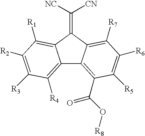
- Other suitable electron transporting materials can be selected from, but are not limited to, a carboxlfluorenone malonitrile of the formula:
- each R is independently selected from the group consisting of hydrogen, alkyl, alkoxy, aryl, halide, halide, and substituted aryl; a nitrated fluoreneone of the formula:
- each R is independently selected from the group consisting of alkyl, alkoxy, aryl, substituted aryl, and halide and wherein at least 2 R groups are nitro;
- a diimide selected from the group consisting of N,N′bis(dialkyl)-1,4,5,8-naphthalenetetracarboxylic diimide and N,N′bis(diaryl)-1,4,5,8-naphthalenetetracarboxylic diimide represented by the formula:
- R1 is alkyl, alkoxy, cycloalkyl, halide, or aryl
- R2 is alkyl, cycloalkyl, or aryl
- each R is independently selected from the group consisting of wherein each R is independently selected from the group consisting of hydrogen, alkyl, alkoxy, aryl, and substituted aryl and halide; a carboxybenzylnaphthaquinone of the alternative formulas:
- each R is independently selected from the group consisting of hydrogen, alkyl, alkoxy, aryl, substituted aryl and halide; a diphenoquinone of the formula:
- each R is independently selected from the group consisting of hydrogen, alkyl, alkoxy, aryl, substituted aryl and halide; and mixtures thereof.
- the electron transporting material can be dispersed in any suitable binder, such as a polymeric binder, and preferably an inert binder.
- suitable binder include those mentioned for the photoconductive overcoat layer, described above.
- the combination of binder and the electron transporting material is selected to be abrasion resistant, or chemically inert, resistant to corona effluent or mechanically robust.
- the overcoating layer is a bipolar transporting layer, preferably an abrasion resistant bipolar transporting layer.
- This overcoating layer can be formed, for example, of electron transporting materials and hole transporting materials dispersed in any suitable binder, such as a polymeric binder, and preferably an inert binder. Any of the above-described binder materials can be used.
- typical organic polymeric film forming binders include, but are not limited to, thermoplastic and thermosetting resins such as polycarbonates, polyesters, polyamides, polyurethanes, polystyrenes, polyarylethers, polyarylsulfones, polybutadienes, polysulfones, polyethersulfones, polyethylenes, polypropylenes, polyimides, polymethylpentenes, polyphenylene sulfides, polyvinyl acetate, polysiloxanes, polyacrylates, polyvinyl acetals, polyamides, polyimides, amino resins, phenylene oxide resins, terephthalic acid resins, phenoxy resins, epoxy resins, phenolic resins, polystyrene and acrylonitrile copolymers, polyvinylchloride, vinylchloride and vinyl acetate copolymers, acrylate copolymers, alkyd resins, cellulosic film formers, thermo
- the bipolar layer is formed preferably as an abrasion resistant bipolar layer.
- This overcoating layer can be formed, for example, of electron transporting and hole transporting materials dispersed in a polymer binder.
- the hole transporting materials used in this embodiment can be suitably selected from any known of after-developed hole transporting materials.
- at least one of the hole transport materials generally comprises an arylamine compound.
- Arylamine hole transport materials can be subdivided into monoamines, diamines, triamines, etc.
- aryl monoamines include but not limited to: N,N-bis(4-methylphenyl)-4-biphenylylamine, N,N-bis(4-methoxyphenyl)-4-biphenylylamine, N,N-bis-(3-methylphenyl)-4-biphenylylamine, N,N-bis(3-methoxyphenyl)-4-biphenylylamine, N,N,N-tri[3-methylphenyl]amine, N,N,N-tri[4-methylphenyl]amine, N,N-di(3-methylphenyl)-p-toluidine, N,N-di(4-methylphenyl)-m-toluidine, and N,N-bis-(3,4-dimethylphenyl)-4-biphenylamine (DBA), and mixtures thereof.
- DBA N,N-bis-(3,4-dimethylphenyl)-4-biphenylamine
- aryl diamines include: those described in U.S. Pat. Nos. 4,306,008, 4,304,829, 4,233,384, 4,115,116, 4,299,897, 4,265,990, 4,081,274 and 6,214,514, each incorporated herein by reference.
- Typical aryl diamine transport compounds include N,N′-diphenyl-N,N′-bis(alkylphenyl)-[1,1′-biphenyl]-4,4′-diamine wherein the alkyl is linear such as for example, methyl, ethyl, propyl, n-butyl and the like, N,N′-diphenyl-N,N′-bis(3-methylphenyl)-[1,1′-biphenyl]-4,4′-diamine, N,N′-diphenyl-N,N′-bis(4-methylphenyl) -[1,1′-biphenyl]-4,4′-diamine, N,N′-diphenyl-N,N′-bis(2-methylphenyl)-[1,1′-biphenyl]-4,4′-diamine, N,N′-diphenyl-N,N′-bis(3-ethylphenyl)-[
- the electron transporting materials for use in this embodiment can be suitably selected from any known of after-developed electron transporting materials.
- said electron transporting material is selected from the group consisting of, but not limited to, a carboxlfluorenone malonitrile of the formula:
- each R is independently selected from the group consisting of hydrogen, alkyl, alkoxy, aryl, halide, halide, and substituted aryl; a nitrated fluoreneone of the formula:
- each R is independently selected from the group consisting of alkyl, alkoxy, aryl, substituted aryl, and halide and wherein at least 2 R groups are nitro;
- a diimide selected from the group consisting of N,N′bis(dialkyl)-1,4,5,8-naphthalenetetracarboxylic diimide and N,N′bis(diaryl)-1,4,5,8-naphthalenetetracarboxylic diimide represented by the formula:
- R1 is alkyl, alkoxy, cycloalkyl, halide, or aryl
- R2 is alkyl, cycloalkyl, or aryl
- each R is independently selected from the group consisting of wherein each R is independently selected from the group consisting of hydrogen, alkyl, alkoxy, aryl, and substituted aryl and halide; a carboxybenzylnaphthaquinone of the alternative formulas:
- each R is independently selected from the group consisting of hydrogen, alkyl, alkoxy, aryl, substituted aryl and halide; a diphenoquinone of the formula:
- each R is independently selected from the group consisting of hydrogen, alkyl, alkoxy, aryl, substituted aryl and halide.
- the electron transporting material can be dispersed in any suitable binder, such as a polymeric binder, and preferably an inert binder.
- suitable binder include those mentioned for the photoconductive overcoat layer, described above.
- the combination of binder and the electron transporting material is selected to be abrasion resistant, or chemically inert, resistant to corona effluent or mechanically robust.
- the overcoating layer is a bipolar transporting layer, preferably an abrasion resistant bipolar transporting layer.
- This overcoating layer can be formed, for example, of electron transporting materials and hole transporting materials dispersed in a silicon binder material.
- electron transporting materials and hole transporting materials can be chemical modified or contain chemical modification to enable them to react directly with the silicon binder material or other electrically inert silicon materials to make up a crosslinked siloxane composition.
- Silicon binder overcoat layers are generally known, and have been disclosed as incorporating charge transport molecules therein.
- an overcoating layer comprising a crosslinked siloxane composition, which is the product of hydrolysis and condensation of at least one silicon-containing compound, is disclosed in U.S. patent application Ser. No. 11/034,062, the entire disclosure of which is incorporated herein by reference.
- the crosslinked siloxane also includes an arylamine hole transport molecule.
- Related disclosures are also included in U.S. patent application Ser. Nos. 11/034,713, 11/034,062, 10/998,585, 10/992,690, 10/992,687, 10/992,658, and 10/938,887, the entire disclosures of which are incorporated herein by reference.
- silicon binder overcoat layers can be further modified, however, to be made bipolar by the incorporation of electron transport materials therein.
- electron transport materials include, but are not limited to, N,N′-bis(1,2-dimethylpropyl)-1,4,5,8-naphthalenetetracarboxylic diimide represented by the following formula
- R and R are independently selected from the group consisting of hydrogen, alkyl with, for example, 1 to about 4 carbon atoms, alkoxy with, for example, 1 to about 4 carbon atoms, and halogen; a quinone selected, for example, from the group consisting of carboxybenzylnaphthaquinone represented by the following formula
- electron transport components are those that are soluble in the solvent matrix illustrated herein, and which components are, for example, carboxyfluorenone malononitrile (CFM) derivatives represented by
- each R is independently selected from the group consisting of hydrogen, alkyl having 1 to about 40 carbon atoms (for example, throughout with respect to the number of carbon atoms), alkoxy having 1 to about 40 carbon atoms, phenyl, substituted phenyl, higher aromatic such as naphthalene and anthracene, alkylphenyl having 6 to about 40 carbons, alkoxyphenyl having 6 to 40 carbons, aryl having 6 to 30 carbons, substituted aryl having 6 to about 30 carbons and halogen; or a nitrated fluorenone derivative represented by
- each R is independently selected from the group consisting of hydrogen, alkyl, alkoxy, aryl, such as phenyl, substituted phenyl, higher aromatics such as naphthalene and anthracene, alkylphenyl, alkoxyphenyl, carbons, substituted aryl and halogen, and wherein at least 2 R groups are nitro; a N,N′-bis(dialkyl)-1,4,5,8-naphthalenetetracarboxylic diimide derivative or N,N′-bis(diaryl)-1,4,5,8-naphthalenetetracarboxylic diimide derivative represented by the general formula/structure
- R 1 is, for example, substituted or unsubstituted alkyl, branched alkyl, cycloalkyl, alkoxy or aryl, such as phenyl, naphthyl, or a higher polycyclic aromatic, such as anthracene
- R 2 is alkyl, branched alkyl, cycloalkyl, or aryl, such as phenyl, naphthyl, or a higher polycyclic aromatics, such as anthracene, or wherein R 2 is the same as R 1 ;
- R 1 and R 2 can independently possess from 1 to about 50 carbons, and more specifically, from 1 and about 12 carbons.
- R 3 , R4, R 5 and R6 are alkyl, branched alkyl, cycloalkyl, alkoxy or aryl, such as phenyl, naphthyl, or a higher polycyclic aromatics such as anthracene or halogen and the like.
- R 3 , R 4 , R 5 and R 6 can be the same or different; a 1,1′-dioxo-2-(aryl)-6-phenyl-4-(dicyanomethylidene)thiopyran
- each R is, for example, independently selected from the group consisting of hydrogen, alkyl with 1 to about 40 carbon atoms, alkoxy with 1 to about 40 carbon atoms, phenyl, substituted phenyl, higher aromatics such as naphthalene and anthracene, alkylphenyl with 6 to about 40 carbons, alkoxyphenyl with 6 to about 40 carbons, aryl with 6 to about 30 carbons, substituted aryl with 6 to about 30 carbons and halogen; a carboxybenzyl naphthaquinone represented by the following
- each R is independently selected from the group consisting of hydrogen, alkyl with 1 to about 40 carbon atoms, alkoxy with 1 to about 40 carbon atoms, phenyl, substituted phenyl, higher aromatics such as naphthalene and anthracene, alkylphenyl with 6 to about 40 carbons, alkoxyphenyl with 6 to about 40 carbons, aryl with 6 to about 30 carbons, substituted aryl with 6 to about 30 carbons and halogen; a diphenoquinone represented by the following
- each of the R substituents are as illustrated herein; or oligomeric and polymeric derivatives in which the above moieties represent part of the oligomer or polymer repeat units, and mixtures thereof wherein the mixtures can contain from 1 to about 99 weight percent of one electron transport component and from about 99 to about 1 weight percent of a second electron transport component, and which electron transports can be dispersed in a resin binder, and wherein the total thereof is about 100 percent.
- the thickness of the continuous overcoat layer selected may depend upon the abrasiveness of the charging (e.g., bias charging roll), cleaning (e.g., blade or web), development (e.g., brush), transfer (e.g., bias transfer roll), etc., system employed and can range up to about 10 micrometers. A thickness of between about 1 micrometer and about 5 micrometers in thickness is preferred. Any suitable and conventional technique may be utilized to mix and thereafter apply the overcoat layer coating mixture to the underlying layer. Typical application techniques include spraying, dip coating, roll coating, wire wound rod coating, and the like. Drying of the deposited coating may be effected by any suitable conventional technique such as oven drying, infrared radiation drying, air drying and the like.
- Ground strips are well known and usually comprise conductive particles dispersed in a film forming binder.
- an anti-curl back coating may be applied to the side opposite the photoreceptor to provide flatness and/or abrasion resistance.
- These overcoating and anti-curl back coating layers are well known in the art and may comprise thermoplastic organic polymers or inorganic polymers that are electrically insulating or slightly semiconductive. Overcoatings are continuous and generally have a thickness of less than about 10 micrometers.
- any suitable conventional electrophotographic charging, exposure, development, transfer, fixing and cleaning techniques may be utilized to form and develop electrostatic latent images on the imaging member of this disclosure.
- conventional light lens or laser exposure systems may be used to form the electrostatic latent image.
- the resulting electrostatic latent image may be developed by suitable conventional development techniques such as magnetic brush, cascade, powder cloud, and the like.
- the imaging members of this disclosure are positive charging imaging members; thus, the charging, exposure, development, transfer, fixing and cleaning techniques in these embodiments are desirably suited for use with such positive charging imaging members.
Landscapes
- Physics & Mathematics (AREA)
- General Physics & Mathematics (AREA)
- Health & Medical Sciences (AREA)
- Emergency Medicine (AREA)
- Photoreceptors In Electrophotography (AREA)
Abstract
Description

wherein each R is independently selected from the group consisting of hydrogen, alkyl, alkoxy, aryl, halide, halide, and substituted aryl; a nitrated fluoreneone of the formula:

wherein each R is independently selected from the group consisting of alkyl, alkoxy, aryl, substituted aryl, and halide and wherein at least 2 R groups are nitro; a diimide selected from the group consisting of N,N′bis(dialkyl)-1,4,5,8-naphthalenetetracarboxylic diimide and N,N′bis(diaryl)-1,4,5,8-naphthalenetetracarboxylic diimide represented by the formula:

wherein R1 is alkyl, alkoxy, cycloalkyl, halide, or aryl; R2 is alkyl, cycloalkyl, or aryl; a 1,1′-dioxo-2-(aryl)-6-phenyl-4-(dicyanomethylidene)thiopyran of the formula:

wherein each R is independently selected from the group consisting of wherein each R is independently selected from the group consisting of hydrogen, alkyl, alkoxy, aryl, and substituted aryl and halide; a carboxybenzylnaphthaquinone of the alternative formulas:

wherein each R is independently selected from the group consisting of hydrogen, alkyl, alkoxy, aryl, substituted aryl and halide; a diphenoquinone of the formula:

wherein each R is independently selected from the group consisting of hydrogen, alkyl, alkoxy, aryl, substituted aryl and halide; and mixtures thereof.
wherein each R is independently selected from the group consisting of hydrogen, alkyl, alkoxy, aryl, halide, halide, and substituted aryl; a nitrated fluoreneone of the formula:

wherein each R is independently selected from the group consisting of alkyl, alkoxy, aryl, substituted aryl, and halide and wherein at least 2 R groups are nitro; a diimide selected from the group consisting of N,N′bis(dialkyl)-1,4,5,8-naphthalenetetracarboxylic diimide and N,N′bis(diaryl)-1,4,5,8-naphthalenetetracarboxylic diimide represented by the formula:

wherein R1 is alkyl, alkoxy, cycloalkyl, halide, or aryl; R2 is alkyl, cycloalkyl, or aryl; a 1,1′-dioxo-2-(aryl)-6-phenyl-4-(dicyanomethylidene)thiopyran of the formula:

wherein each R is independently selected from the group consisting of wherein each R is independently selected from the group consisting of hydrogen, alkyl, alkoxy, aryl, and substituted aryl and halide; a carboxybenzylnaphthaquinone of the alternative formulas:

wherein each R is independently selected from the group consisting of hydrogen, alkyl, alkoxy, aryl, substituted aryl and halide; a diphenoquinone of the formula:

and mixtures thereof, wherein each R is independently selected from the group consisting of hydrogen, alkyl, alkoxy, aryl, substituted aryl and halide.

1,1′-dioxo-2-(4-methylphenyl)-6-phenyl-4-(dicyanomethylidene)thiopyran represented by the following formula

wherein R and R are independently selected from the group consisting of hydrogen, alkyl with, for example, 1 to about 4 carbon atoms, alkoxy with, for example, 1 to about 4 carbon atoms, and halogen; a quinone selected, for example, from the group consisting of carboxybenzylnaphthaquinone represented by the following formula

tetra(t-butyl) diphenolquinone represented by the following formula

mixtures thereof, and the like; the butoxy derivative of carboxyfluorenone malononitrile; the 2-ethylhexanol of carboxyfluorenone malononitrile; the 2-heptyl derivative of N,N′-bis(1,2-diethylpropyl)-1,4,5,8-naphthalenetetracarboxylic diimide; and the sec-isobutyl and n-butyl derivatives of 1,1-(N,N′-bisalkyl-bis-4-phthalimido)-2,2-biscyano-ethylene.

wherein each R is independently selected from the group consisting of hydrogen, alkyl having 1 to about 40 carbon atoms (for example, throughout with respect to the number of carbon atoms), alkoxy having 1 to about 40 carbon atoms, phenyl, substituted phenyl, higher aromatic such as naphthalene and anthracene, alkylphenyl having 6 to about 40 carbons, alkoxyphenyl having 6 to 40 carbons, aryl having 6 to 30 carbons, substituted aryl having 6 to about 30 carbons and halogen; or a nitrated fluorenone derivative represented by

wherein each R is independently selected from the group consisting of hydrogen, alkyl, alkoxy, aryl, such as phenyl, substituted phenyl, higher aromatics such as naphthalene and anthracene, alkylphenyl, alkoxyphenyl, carbons, substituted aryl and halogen, and wherein at least 2 R groups are nitro; a N,N′-bis(dialkyl)-1,4,5,8-naphthalenetetracarboxylic diimide derivative or N,N′-bis(diaryl)-1,4,5,8-naphthalenetetracarboxylic diimide derivative represented by the general formula/structure

wherein R1 is, for example, substituted or unsubstituted alkyl, branched alkyl, cycloalkyl, alkoxy or aryl, such as phenyl, naphthyl, or a higher polycyclic aromatic, such as anthracene; R2 is alkyl, branched alkyl, cycloalkyl, or aryl, such as phenyl, naphthyl, or a higher polycyclic aromatics, such as anthracene, or wherein R2 is the same as R1; R1 and R2 can independently possess from 1 to about 50 carbons, and more specifically, from 1 and about 12 carbons. R3, R4, R5 and R6 are alkyl, branched alkyl, cycloalkyl, alkoxy or aryl, such as phenyl, naphthyl, or a higher polycyclic aromatics such as anthracene or halogen and the like. R3, R4, R5 and R6 can be the same or different; a 1,1′-dioxo-2-(aryl)-6-phenyl-4-(dicyanomethylidene)thiopyran

wherein each R is, for example, independently selected from the group consisting of hydrogen, alkyl with 1 to about 40 carbon atoms, alkoxy with 1 to about 40 carbon atoms, phenyl, substituted phenyl, higher aromatics such as naphthalene and anthracene, alkylphenyl with 6 to about 40 carbons, alkoxyphenyl with 6 to about 40 carbons, aryl with 6 to about 30 carbons, substituted aryl with 6 to about 30 carbons and halogen; a carboxybenzyl naphthaquinone represented by the following

wherein each R is independently selected from the group consisting of hydrogen, alkyl with 1 to about 40 carbon atoms, alkoxy with 1 to about 40 carbon atoms, phenyl, substituted phenyl, higher aromatics such as naphthalene and anthracene, alkylphenyl with 6 to about 40 carbons, alkoxyphenyl with 6 to about 40 carbons, aryl with 6 to about 30 carbons, substituted aryl with 6 to about 30 carbons and halogen; a diphenoquinone represented by the following

and mixtures thereof, wherein each of the R substituents are as illustrated herein; or oligomeric and polymeric derivatives in which the above moieties represent part of the oligomer or polymer repeat units, and mixtures thereof wherein the mixtures can contain from 1 to about 99 weight percent of one electron transport component and from about 99 to about 1 weight percent of a second electron transport component, and which electron transports can be dispersed in a resin binder, and wherein the total thereof is about 100 percent.
Claims (18)


Priority Applications (1)
| Application Number | Priority Date | Filing Date | Title |
|---|---|---|---|
| US11/191,048 US7491989B2 (en) | 2005-07-28 | 2005-07-28 | Positive charging photoreceptor |
Applications Claiming Priority (1)
| Application Number | Priority Date | Filing Date | Title |
|---|---|---|---|
| US11/191,048 US7491989B2 (en) | 2005-07-28 | 2005-07-28 | Positive charging photoreceptor |
Publications (2)
| Publication Number | Publication Date |
|---|---|
| US20070023747A1 US20070023747A1 (en) | 2007-02-01 |
| US7491989B2 true US7491989B2 (en) | 2009-02-17 |
Family
ID=37693338
Family Applications (1)
| Application Number | Title | Priority Date | Filing Date |
|---|---|---|---|
| US11/191,048 Expired - Fee Related US7491989B2 (en) | 2005-07-28 | 2005-07-28 | Positive charging photoreceptor |
Country Status (1)
| Country | Link |
|---|---|
| US (1) | US7491989B2 (en) |
Cited By (5)
| Publication number | Priority date | Publication date | Assignee | Title |
|---|---|---|---|---|
| US20080008958A1 (en) * | 2006-07-05 | 2008-01-10 | Leonhard Kurz Gmbh & Co. Kg | Signing film |
| US20110111334A1 (en) * | 2009-11-06 | 2011-05-12 | Xerox Corporation | Light shock resistant overcoat layer |
| US9125829B2 (en) | 2012-08-17 | 2015-09-08 | Hallstar Innovations Corp. | Method of photostabilizing UV absorbers, particularly dibenzyolmethane derivatives, e.g., Avobenzone, with cyano-containing fused tricyclic compounds |
| US9145383B2 (en) | 2012-08-10 | 2015-09-29 | Hallstar Innovations Corp. | Compositions, apparatus, systems, and methods for resolving electronic excited states |
| US9867800B2 (en) | 2012-08-10 | 2018-01-16 | Hallstar Innovations Corp. | Method of quenching singlet and triplet excited states of pigments, such as porphyrin compounds, particularly protoporphyrin IX, with conjugated fused tricyclic compounds have electron withdrawing groups, to reduce generation of reactive oxygen species, particularly singlet oxygen |
Families Citing this family (3)
| Publication number | Priority date | Publication date | Assignee | Title |
|---|---|---|---|---|
| WO2005124453A2 (en) | 2004-06-14 | 2005-12-29 | Georgia Tech Research Corporation | Perylene charge-transport materials, methods of fabrication thereof, and methods of use thereof |
| US20100239967A1 (en) * | 2009-03-20 | 2010-09-23 | Xerox Corporation | Overcoat layer comprising metal oxides |
| US8680515B2 (en) * | 2011-05-03 | 2014-03-25 | Xerox Corporation | Digital marking using a bipolar imaging member |
Citations (32)
| Publication number | Priority date | Publication date | Assignee | Title |
|---|---|---|---|---|
| US2886434A (en) | 1955-06-06 | 1959-05-12 | Horizons Inc | Protected photoconductive element and method of making same |
| US3121006A (en) | 1957-06-26 | 1964-02-11 | Xerox Corp | Photo-active member for xerography |
| US3357989A (en) | 1965-10-29 | 1967-12-12 | Xerox Corp | Metal free phthalocyanine in the new x-form |
| US3397982A (en) | 1964-12-21 | 1968-08-20 | Xerox Corp | Xerographic plate with an inorganic glass binder having an overcoating consisting essentially of aluminum oxide |
| US3442781A (en) | 1966-01-06 | 1969-05-06 | Xerox Corp | Photoelectrophoretic and xerographic imaging processes employing triphenodioxazines as the electrically photosensitive component |
| US3655377A (en) | 1966-10-03 | 1972-04-11 | Xerox Corp | Tri-layered selenium doped photoreceptor |
| US4081274A (en) | 1976-11-01 | 1978-03-28 | Xerox Corporation | Composite layered photoreceptor |
| US4115116A (en) | 1976-04-02 | 1978-09-19 | Xerox Corporation | Imaging member having a polycarbonate-biphenyl diamine charge transport layer |
| US4233384A (en) | 1979-04-30 | 1980-11-11 | Xerox Corporation | Imaging system using novel charge transport layer |
| US4265990A (en) | 1977-05-04 | 1981-05-05 | Xerox Corporation | Imaging system with a diamine charge transport material in a polycarbonate resin |
| US4299897A (en) | 1978-12-15 | 1981-11-10 | Xerox Corporation | Aromatic amino charge transport layer in electrophotography |
| US4304829A (en) | 1977-09-22 | 1981-12-08 | Xerox Corporation | Imaging system with amino substituted phenyl methane charge transport layer |
| US4306008A (en) | 1978-12-04 | 1981-12-15 | Xerox Corporation | Imaging system with a diamine charge transport material in a polycarbonate resin |
| US4415639A (en) | 1982-09-07 | 1983-11-15 | Xerox Corporation | Multilayered photoresponsive device for electrophotography |
| US4420547A (en) | 1980-10-16 | 1983-12-13 | Olympus Optical Company Ltd. | Photosensitive member for electrophotography having ultraviolet absorption layer |
| US4647521A (en) | 1983-09-08 | 1987-03-03 | Canon Kabushiki Kaisha | Image-holding member having top layer of hydrophobic silica |
| US4664995A (en) | 1985-10-24 | 1987-05-12 | Xerox Corporation | Electrostatographic imaging members |
| US4675262A (en) | 1985-01-16 | 1987-06-23 | Canon Kabushiki Kaisha | Multilayer electrophotographic photosensitive element having charge transport layer containing powdered material having specified refractive index |
| US4678731A (en) | 1985-06-25 | 1987-07-07 | Kabushiki Kaisha Toshiba | Electrophotographic photosensitive member having barrier layer comprising microcrystalline silicon containing hydrogen |
| US4713308A (en) | 1985-06-25 | 1987-12-15 | Kabushiki Kaisha Toshiba | Electrophotographic photosensitive member using microcrystalline silicon |
| US4717637A (en) | 1985-06-25 | 1988-01-05 | Kabushiki Kaisha Toshiba | Electrophotographic photosensitive member using microcrystalline silicon |
| US4784928A (en) | 1986-09-02 | 1988-11-15 | Eastman Kodak Company | Reusable electrophotographic element |
| US4855203A (en) | 1987-08-31 | 1989-08-08 | Xerox Corporation | Imaging members with photogenerating compositions obtained by solution processes |
| US4869982A (en) | 1987-04-30 | 1989-09-26 | X-Solve, Inc. | Electrophotographic photoreceptor containing a toner release material |
| US5008167A (en) | 1989-12-15 | 1991-04-16 | Xerox Corporation | Internal metal oxide filled materials for electrophotographic devices |
| US5096795A (en) | 1990-04-30 | 1992-03-17 | Xerox Corporation | Multilayered photoreceptor containing particulate materials |
| US5521047A (en) | 1995-05-31 | 1996-05-28 | Xerox Corporation | Process for preparing a multilayer electrophotographic imaging member |
| US5707767A (en) | 1996-11-19 | 1998-01-13 | Xerox Corporation | Mechanically robust electrophotographic imaging member free of interference fringes |
| US5709974A (en) | 1996-09-27 | 1998-01-20 | Xerox Corporation | High speed electrophotographic imaging member |
| US5891594A (en) | 1997-01-13 | 1999-04-06 | Xerox Corporation | Process for preparing electrophotographic imaging member with perylene-containing charge-generating material and n-butylacetate |
| US6214514B1 (en) | 1999-09-29 | 2001-04-10 | Xerox Corporation | Process for fabricating electrophotographic imaging member |
| US6410196B1 (en) * | 2001-09-28 | 2002-06-25 | Xerox Corporation | Photoreceptor charge transport layer with a polycarbonate binder |
-
2005
- 2005-07-28 US US11/191,048 patent/US7491989B2/en not_active Expired - Fee Related
Patent Citations (32)
| Publication number | Priority date | Publication date | Assignee | Title |
|---|---|---|---|---|
| US2886434A (en) | 1955-06-06 | 1959-05-12 | Horizons Inc | Protected photoconductive element and method of making same |
| US3121006A (en) | 1957-06-26 | 1964-02-11 | Xerox Corp | Photo-active member for xerography |
| US3397982A (en) | 1964-12-21 | 1968-08-20 | Xerox Corp | Xerographic plate with an inorganic glass binder having an overcoating consisting essentially of aluminum oxide |
| US3357989A (en) | 1965-10-29 | 1967-12-12 | Xerox Corp | Metal free phthalocyanine in the new x-form |
| US3442781A (en) | 1966-01-06 | 1969-05-06 | Xerox Corp | Photoelectrophoretic and xerographic imaging processes employing triphenodioxazines as the electrically photosensitive component |
| US3655377A (en) | 1966-10-03 | 1972-04-11 | Xerox Corp | Tri-layered selenium doped photoreceptor |
| US4115116A (en) | 1976-04-02 | 1978-09-19 | Xerox Corporation | Imaging member having a polycarbonate-biphenyl diamine charge transport layer |
| US4081274A (en) | 1976-11-01 | 1978-03-28 | Xerox Corporation | Composite layered photoreceptor |
| US4265990A (en) | 1977-05-04 | 1981-05-05 | Xerox Corporation | Imaging system with a diamine charge transport material in a polycarbonate resin |
| US4304829A (en) | 1977-09-22 | 1981-12-08 | Xerox Corporation | Imaging system with amino substituted phenyl methane charge transport layer |
| US4306008A (en) | 1978-12-04 | 1981-12-15 | Xerox Corporation | Imaging system with a diamine charge transport material in a polycarbonate resin |
| US4299897A (en) | 1978-12-15 | 1981-11-10 | Xerox Corporation | Aromatic amino charge transport layer in electrophotography |
| US4233384A (en) | 1979-04-30 | 1980-11-11 | Xerox Corporation | Imaging system using novel charge transport layer |
| US4420547A (en) | 1980-10-16 | 1983-12-13 | Olympus Optical Company Ltd. | Photosensitive member for electrophotography having ultraviolet absorption layer |
| US4415639A (en) | 1982-09-07 | 1983-11-15 | Xerox Corporation | Multilayered photoresponsive device for electrophotography |
| US4647521A (en) | 1983-09-08 | 1987-03-03 | Canon Kabushiki Kaisha | Image-holding member having top layer of hydrophobic silica |
| US4675262A (en) | 1985-01-16 | 1987-06-23 | Canon Kabushiki Kaisha | Multilayer electrophotographic photosensitive element having charge transport layer containing powdered material having specified refractive index |
| US4717637A (en) | 1985-06-25 | 1988-01-05 | Kabushiki Kaisha Toshiba | Electrophotographic photosensitive member using microcrystalline silicon |
| US4678731A (en) | 1985-06-25 | 1987-07-07 | Kabushiki Kaisha Toshiba | Electrophotographic photosensitive member having barrier layer comprising microcrystalline silicon containing hydrogen |
| US4713308A (en) | 1985-06-25 | 1987-12-15 | Kabushiki Kaisha Toshiba | Electrophotographic photosensitive member using microcrystalline silicon |
| US4664995A (en) | 1985-10-24 | 1987-05-12 | Xerox Corporation | Electrostatographic imaging members |
| US4784928A (en) | 1986-09-02 | 1988-11-15 | Eastman Kodak Company | Reusable electrophotographic element |
| US4869982A (en) | 1987-04-30 | 1989-09-26 | X-Solve, Inc. | Electrophotographic photoreceptor containing a toner release material |
| US4855203A (en) | 1987-08-31 | 1989-08-08 | Xerox Corporation | Imaging members with photogenerating compositions obtained by solution processes |
| US5008167A (en) | 1989-12-15 | 1991-04-16 | Xerox Corporation | Internal metal oxide filled materials for electrophotographic devices |
| US5096795A (en) | 1990-04-30 | 1992-03-17 | Xerox Corporation | Multilayered photoreceptor containing particulate materials |
| US5521047A (en) | 1995-05-31 | 1996-05-28 | Xerox Corporation | Process for preparing a multilayer electrophotographic imaging member |
| US5709974A (en) | 1996-09-27 | 1998-01-20 | Xerox Corporation | High speed electrophotographic imaging member |
| US5707767A (en) | 1996-11-19 | 1998-01-13 | Xerox Corporation | Mechanically robust electrophotographic imaging member free of interference fringes |
| US5891594A (en) | 1997-01-13 | 1999-04-06 | Xerox Corporation | Process for preparing electrophotographic imaging member with perylene-containing charge-generating material and n-butylacetate |
| US6214514B1 (en) | 1999-09-29 | 2001-04-10 | Xerox Corporation | Process for fabricating electrophotographic imaging member |
| US6410196B1 (en) * | 2001-09-28 | 2002-06-25 | Xerox Corporation | Photoreceptor charge transport layer with a polycarbonate binder |
Non-Patent Citations (7)
| Title |
|---|
| U.S. Appl. No. 10/938,887. |
| U.S. Appl. No. 10/992,658. |
| U.S. Appl. No. 10/992,687. |
| U.S. Appl. No. 10/992,690. |
| U.S. Appl. No. 10/998,585. |
| U.S. Appl. No. 11/034,062. |
| U.S. Appl. No. 11/034,713. |
Cited By (11)
| Publication number | Priority date | Publication date | Assignee | Title |
|---|---|---|---|---|
| US20080008958A1 (en) * | 2006-07-05 | 2008-01-10 | Leonhard Kurz Gmbh & Co. Kg | Signing film |
| US7773162B2 (en) * | 2006-07-05 | 2010-08-10 | Leonhard Kurz Stiftung & Co. Kg | Signing film |
| US20110111334A1 (en) * | 2009-11-06 | 2011-05-12 | Xerox Corporation | Light shock resistant overcoat layer |
| US8367285B2 (en) * | 2009-11-06 | 2013-02-05 | Xerox Corporation | Light shock resistant overcoat layer |
| US9145383B2 (en) | 2012-08-10 | 2015-09-29 | Hallstar Innovations Corp. | Compositions, apparatus, systems, and methods for resolving electronic excited states |
| US9611246B2 (en) | 2012-08-10 | 2017-04-04 | Hallstar Innovations Corp. | Compositions, apparatus, systems, and methods for resolving electronic excited states |
| US9765051B2 (en) | 2012-08-10 | 2017-09-19 | Hallstar Innovations Corp. | Compositions, apparatus, systems, and methods for resolving electronic excited states |
| US9867800B2 (en) | 2012-08-10 | 2018-01-16 | Hallstar Innovations Corp. | Method of quenching singlet and triplet excited states of pigments, such as porphyrin compounds, particularly protoporphyrin IX, with conjugated fused tricyclic compounds have electron withdrawing groups, to reduce generation of reactive oxygen species, particularly singlet oxygen |
| US9926289B2 (en) | 2012-08-10 | 2018-03-27 | Hallstar Innovations Corp. | Compositions, apparatus, systems, and methods for resolving electronic excited states |
| US10632096B2 (en) | 2012-08-10 | 2020-04-28 | HallStar Beauty and Personal Care Innovations Company | Method of quenching singlet and triplet excited states of photodegradable pigments, such as porphyrin compounds, particularly protoporphyrin IX, with conjugated fused tricyclic compounds having electron withdrawing groups, to reduce generation of singlet oxygen |
| US9125829B2 (en) | 2012-08-17 | 2015-09-08 | Hallstar Innovations Corp. | Method of photostabilizing UV absorbers, particularly dibenzyolmethane derivatives, e.g., Avobenzone, with cyano-containing fused tricyclic compounds |
Also Published As
| Publication number | Publication date |
|---|---|
| US20070023747A1 (en) | 2007-02-01 |
Similar Documents
| Publication | Publication Date | Title |
|---|---|---|
| US5830614A (en) | Multilayer organic photoreceptor employing a dual layer of charge transporting polymers | |
| US8883384B2 (en) | Binderless overcoat layer | |
| US6835512B2 (en) | Electrophotographic photosensitive member, process cartridge and electrophotographic apparatus | |
| US5055366A (en) | Polymeric protective overcoatings contain hole transport material for electrophotographic imaging members | |
| US6300027B1 (en) | Low surface energy photoreceptors | |
| US7491989B2 (en) | Positive charging photoreceptor | |
| EP1918779A1 (en) | Photoreceptor containing substituted biphenyl diamine and method of forming same | |
| EP1291724B1 (en) | Blue diode laser sensitive electrophotographic photoreceptor | |
| EP0585668B1 (en) | Photoconductors employing sensitized extrinsic photogenerating pigments | |
| US8263300B2 (en) | Electrophotographic photoconductor, image forming apparatus, and process cartridge | |
| US8029958B2 (en) | Overcoat layer in photoreceptive device | |
| US7476479B2 (en) | Hydrolyzed semi-conductive nanoparticles for imaging member undercoating layers | |
| US7309551B2 (en) | Electron conductive overcoat layer for photoreceptors | |
| CA2595825C (en) | Photoreceptor | |
| US7691551B2 (en) | Imaging member | |
| EP1076265B1 (en) | Electrophotographic photosensitive member, process cartridge, and electrophotographic apparatus | |
| US8034518B2 (en) | Photoreceptor | |
| US20070059620A1 (en) | High sensitive imaging member with intermediate and/or undercoat layer | |
| US20070059616A1 (en) | Coated substrate for photoreceptor | |
| CA2595822C (en) | Photoreceptor | |
| US6969573B2 (en) | Blue diode laser sensitive photoreceptor | |
| US5230974A (en) | Photoreceptor for textual and pictorial reproductions having a noncontinuous charge generating layer | |
| US7384718B2 (en) | Charge generating composition and imaging member | |
| US7662528B2 (en) | Charge generating composition | |
| US7390598B2 (en) | Photoreceptor with three-layer photoconductive layer |
Legal Events
| Date | Code | Title | Description |
|---|---|---|---|
| AS | Assignment |
Owner name: XEROX CORPORATION, CONNECTICUT Free format text: ASSIGNMENT OF ASSIGNORS INTEREST;ASSIGNORS:LOUTFY, RAFIK O.;POPOVIC, ZORAN D.;GRAHAM, JOHN;AND OTHERS;REEL/FRAME:016831/0194;SIGNING DATES FROM 20050725 TO 20050726 |
|
| FEPP | Fee payment procedure |
Free format text: PAYOR NUMBER ASSIGNED (ORIGINAL EVENT CODE: ASPN); ENTITY STATUS OF PATENT OWNER: LARGE ENTITY |
|
| STCF | Information on status: patent grant |
Free format text: PATENTED CASE |
|
| FPAY | Fee payment |
Year of fee payment: 4 |
|
| FPAY | Fee payment |
Year of fee payment: 8 |
|
| FEPP | Fee payment procedure |
Free format text: MAINTENANCE FEE REMINDER MAILED (ORIGINAL EVENT CODE: REM.); ENTITY STATUS OF PATENT OWNER: LARGE ENTITY |
|
| LAPS | Lapse for failure to pay maintenance fees |
Free format text: PATENT EXPIRED FOR FAILURE TO PAY MAINTENANCE FEES (ORIGINAL EVENT CODE: EXP.); ENTITY STATUS OF PATENT OWNER: LARGE ENTITY |
|
| STCH | Information on status: patent discontinuation |
Free format text: PATENT EXPIRED DUE TO NONPAYMENT OF MAINTENANCE FEES UNDER 37 CFR 1.362 |
|
| FP | Lapsed due to failure to pay maintenance fee |
Effective date: 20210217 |