US7486130B2 - Clock skew compensation - Google Patents
Clock skew compensation Download PDFInfo
- Publication number
- US7486130B2 US7486130B2 US11/610,943 US61094306A US7486130B2 US 7486130 B2 US7486130 B2 US 7486130B2 US 61094306 A US61094306 A US 61094306A US 7486130 B2 US7486130 B2 US 7486130B2
- Authority
- US
- United States
- Prior art keywords
- circuit
- clock
- voltage source
- supply voltage
- distribution network
- Prior art date
- Legal status (The legal status is an assumption and is not a legal conclusion. Google has not performed a legal analysis and makes no representation as to the accuracy of the status listed.)
- Expired - Fee Related
Links
Images


Classifications
-
- G—PHYSICS
- G06—COMPUTING OR CALCULATING; COUNTING
- G06F—ELECTRIC DIGITAL DATA PROCESSING
- G06F30/00—Computer-aided design [CAD]
- G06F30/30—Circuit design
- G06F30/39—Circuit design at the physical level
- G06F30/396—Clock trees
-
- G—PHYSICS
- G06—COMPUTING OR CALCULATING; COUNTING
- G06F—ELECTRIC DIGITAL DATA PROCESSING
- G06F30/00—Computer-aided design [CAD]
- G06F30/30—Circuit design
Definitions
- the invention relates to clock skew compensation.
- Digital circuits include circuit elements that function according to a clock signal that is distributed throughout the circuit by a clock distribution network.
- the topology of the clock distribution network is that of a tree.
- a clock tree has a clock source at the root of the tree and circuit elements at the leaves of the tree.
- the nodes of the clock tree are buffers (signal driving circuit elements) that drive some number of sinks.
- a sink can be a leaf circuit element or a buffer circuit element driving a sub-tree.
- the structure of a clock tree can be described according to levels. Each node other than the root is connected to a “parent” node by a link in a graph representing the tree.
- the root of a tree is at level 0.
- the nodes directly connected to the root are at level 1.
- the nodes directly connected to nodes at level L are at level L+1.
- the level of a node is the number of links between the root and that node.
- the largest level is the depth D of the tree. Since a buffer has a limit to the number of sinks that it can drive (the “fanout” limit), an increase in the number of circuit elements driven by a clock tree, in some cases, calls for an increase in the depth of the clock tree.
- the buffers in a clock tree introduce delay in the clock signal provided to a circuit element with respect to a reference clock signal (e.g., the signal at the root source node).
- Clock tree synthesis techniques are used to balance delay in different portions of a clock distribution network to meet setup and hold times for bistable multivibrator circuit elements such as flip-flops or latches. In some cases, this calls for reducing skew between clock signals at the inputs of circuit elements.
- the rising edge of the clock supplied to the first flip-flop should be close enough to the rising edge of the clock supplied to the second-flip for the signal propagated between the flip-flops to meet the setup and hold time requirements of the second flip-flop.
- Balancing delays in a circuit can involve adding delay (e.g., with delay buffers) in logic paths of the circuit.
- the clock distribution network is designed such that “useful skew” between clock inputs supplied to circuit elements is used to compensate for circuit delays to meet setup and hold times and improve overall system performance.
- Other techniques can be used to synchronize clock signals in a digital system, including using phase-locked loops to synchronize clock signals for different portions of a circuit.
- the invention features an integrated circuit.
- the integrated circuit includes a first clock distribution network distributing a first clock signal to a first set of circuit elements and a second clock distribution network distributing a second clock signal to a second set of circuit elements.
- the first set of circuit elements and at least a portion of the first clock distribution network are located in a portion of the circuit characterized by a first circuit characteristic.
- the second set of circuit elements and at least a portion of the second clock distribution network are located in a portion of the circuit characterized by a second circuit characteristic different from the first circuit characteristic.
- the second clock distribution network includes a source of the second clock signal derived from a portion of the first clock distribution network located in the portion of the circuit characterized by the second circuit characteristic.
- the invention features a method including distributing a clock signal from a clock tree to a first set of circuit elements characterized by a first circuit characteristic; and distributing a clock signal from a sub-tree of the clock tree to a second set of circuit elements characterized by a second circuit characteristic different from the first circuit characteristic.
- aspects of the invention can include one or more of the following features.
- the first and second circuit characteristics comprise different average clock signal delays.
- the first and second circuit characteristics comprise different clock signal delay variations.
- the first circuit characteristic comprises a first supply voltage source for the first set of circuit elements
- the second circuit characteristic comprises a second supply voltage source for the second set of circuit elements.
- the first supply voltage source comprises a varying supply voltage source
- the second supply voltage source comprises a substantially fixed supply voltage source
- the substantially fixed supply voltage source comprises a regulated voltage source.
- the varying supply voltage source comprises at least one battery.
- the first clock distribution network has a tree topology.
- the second clock distribution network has a tree topology.
- the first and second sets of circuit elements each include at least one bistable multivibrator circuit element.
- At least one bistable multivibrator circuit element in the second set provides an input signal for a bistable multivibrator circuit element in the first set.
- At least one bistable multivibrator circuit element in the first set provides an input signal for a bistable multivibrator circuit element in the second set.
- the input signal is derived from an output of the bistable multivibrator circuit element in the second set after propagating through one or more logic gates.
- aspects of the invention can include one or more of the following advantages.
- the clock distribution approach can improve a designer's ability to balance clock trees in different voltage domains such that it is possible to meet hold times in both directions without necessarily needing to add large delays.
- the approach controls the relative timing of clock signals at the roots of clock trees in the different voltage domains. Only small variations then remain to be compensated, which can be accomplished by adding small delays. Paths that cross from one domain to another in both directions can be made to meet hold times.
- FIGS. 1 , 3 and 4 are circuit diagrams.
- FIGS. 2 , 5 and 6 are timing diagrams.
- the delays through circuit elements or logic gates can be subject to large variations due to temperature, voltage and silicon processing variations.
- the temperature and processing variation across the die are usually small, it is sometimes desirable to have different physical parts of the IC operating at different supply voltages. This difference in supply voltage can lead to large differences in delays between different parts of the IC.
- this variation in delay can be compensated by appropriate design of the interface between parts of the IC that operate at different voltages. However, in some cases this may not be possible.
- One situation where the variations in delay can be a problem is where data is transferred between flip-flops in each part of the IC.
- Setup time is the time by which input data must arrive before the clock. This is met by limiting the total delay between one flip-flop's output and the next flip-flop's input. Even with large differences in clock network delay it is normally possible to meet this requirement given a fast enough base technology.
- Hold time is the time that data on one flip-flop's output must remain stable after a clock edge in order to be reliably captured by the next flip-flop.
- the hold time In an IC design in which the clock trees are fully balanced it is usually possible to meet the hold time by inserting small delays (e.g., with delay buffers) between flip-flops connected together.
- a circuit 100 includes a flip-flop 102 A located in a first circuit domain 101 whose output is connected through one or more logic elements 104 to the input of a flip-flop 102 B located in a second circuit domain 103 .
- a conceptual interface 108 between the first circuit domain 101 and the second circuit domain 103 represents a separation between a portion of the circuit 100 characterized by relatively small variations in clock signal delay of the first domain 101 , and a portion of the circuit 100 characterized by larger and/or more variable clock signal delays of the second domain 103 .
- a flip-flop 102 C located in the second circuit domain 103 has an output connected through one or more logic elements 112 to the input of a flip-flop 102 D in the first circuit domain 101 .
- a clock distribution network for the circuit 100 includes a clock input 106 that receives a source clock signal, and buffers 110 A, 110 B, and 110 C that distribute the clock signal to the flip-flops 102 A, 102 B, 102 C, and 102 D.
- a large delay in the clock signal in the second domain 103 relative to the clock signal in the first domain 101 can lead to a violation in hold time. If this clock skew is small, flip-flop 102 A transfers data to flip-flop 102 B and observes the hold time at flip-flop 102 B's input. If the delays in the logic elements 104 in the path between flip-flop 102 A and flip-flop 102 B are small and the clock skew is large then this hold time may not be met.
- the hold time is met in this case because of the skew between the clocks, which in this direction helps to meet the hold time.
- the setup time can be met by limiting the delay caused by logic elements 112 on the path between flip-flop 102 C and flip-flop 102 D.
- the timing diagram in FIG. 2 shows the timing of clock and data signals for exemplary clock skew delays in the clock distribution network of the circuit 100 .
- a plot labeled Clk 1 shows the clock signal provided to the flip-flops 102 A and 102 D in the first circuit domain 101 .
- a plot labeled Clk 2 shows the clock signal provided to the flip-flops 102 B and 102 C in the second circuit domain 103 , where rising edge of the clock signal Clk 2 is delayed with respect to the rising edge of the clock signal Clk 1 by a clock skew delay t skew .
- a plot labeled A/Q shows the output signal from flip-flop 102 A.
- a plot labeled B/D shows the input signal provided to flip-flop 102 B.
- a plot labeled C/Q shows the output signal from flip-flop 102 C.
- a plot labeled D/D shows the input signal provided to flip-flop 102 D.
- the clock skew delay t skew is large enough such that the hold time t hold is not met for flip-flip 102 B.
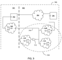
- a clock distribution approach used in a circuit 300 includes a first circuit element 302 located in a first circuit domain 301 characterized by relatively small variations in clock signal delay.
- the first circuit element 302 is connected (optionally through logic 304 ) to a second circuit element 306 located in a second circuit domain 303 characterized by larger and/or more variable clock signal delays.
- a clock tree 308 in the second domain 303 includes a first portion 310 connected to a buffer 312 feeding a first subtree 314 and a second subtree 316 .
- a clock tree 320 in the first domain 301 has a root that is taken from a portion of the clock tree 308 in the second domain 303 .
- FIG. 4 shows an exemplary circuit 400 that uses this clock distribution approach.
- a first domain 401 uses a fixed source voltage that contributes to relatively small variations in clock signal delay. Though there may still be some variation in the clock signal delay in the first domain 401 due to changes in operating temperature, for example.
- a second domain 403 uses a varying source voltage that contributes to larger and more variable clock signal delays.
- a conceptual interface 408 separates the first circuit domain 401 and the second circuit domain 403 .
- the circuit 400 includes a flip-flop 402 A located in the first circuit domain 101 whose output is connected through one or more logic elements 404 to the input of a flip-flop 402 B located in a second circuit domain 403 .
- a flip-flop 402 C located in the second circuit domain 403 has an output connected through one or more logic elements 412 to the input of a flip-flop 402 D in the first circuit domain 401 .
- a clock distribution network for the circuit 400 includes a clock input 406 that receives a source clock signal.
- the clock distribution network includes a voltage level translator 414 A to translate the clock signal voltage from the first circuit domain 401 to the second circuit domain 403 , and a voltage level translator 414 B to translate the clock signal voltage from the second circuit domain 403 to the first circuit domain 401 .
- a clock tree 420 distributes a clock signal from the root of the tree 420 to circuit elements in the second circuit domain 403 including the flip-flops 402 B and 402 C.
- a clock tree 422 distributes a clock signal from the root of the tree 422 to circuit elements in the first circuit domain 401 including the flip-flops 402 A and 402 D.
- the root clock signal distributed by the clock tree 422 is derived from a voltage translated clock signal taken from a portion of the clock tree 420 located in the second circuit domain 403 (e.g., taken from a level of the clock tree 420 that is below the root and above the depth of the clock tree 420 ).
- the timing diagram in FIG. 5 shows the relationship between the clocks under “small variation case” (i.e., the case in which delay variations across the IC are small) and “large variation case” (i.e., the case in which delay variations across the IC are large) conditions as well as the “average case” (i.e., the case in which delay variations are average).
- the plots shown in FIG. 5 show relative time positions for the rising edge of the clock signals in different portions if the circuit 400 .
- the reference clock ClkRef corresponds to the source clock signal at the clock input 402 .
- the pair of clock signals Clk 1 S and Clk 2 S correspond to clock signals for elements in the first and second domains, respectively, in the small variation case.
- the pair of clock signals Clk 1 L and Clk 2 L correspond to clock signals for elements in the first and second domains, respectively, in the large variation case.
- the pair of clock signals Clk 1 A and Clk 2 A that correspond to the average case represent the case of equal delay from the clock input 402 to the end points of the distributed clock networks for the first and second domains, respectively.
- the root of the clock network supplied to the first domain 401 can be taken from a selected stage of the clock network supplied to the second domain 403 so that the clock signals in the first domain are delayed by the majority of the delay experienced by the clock signals in the second domain to remove the bulk of the difference between them. This leaves only a small amount of delay difference between the clock networks that cannot be “trimmed out” in this way. This residual uncertainty can be centered about the ideal zero delay difference by careful choice of the tap point 424 .
- the clock tree 420 has a delay that is determined by a delay per level of D v with n levels.
- the clock tree 422 is tapped after n ⁇ x levels of the clock tree 420 , and the additional delay in the first domain 401 is determined by a delay per level of D f with m levels.
- the clock skew is then given by: mD f ⁇ xD v .
- the clock delays in the first and second domains are smaller (e.g., 2.5 ns per level for the variable domain and 0.5 ns per level for the fixed domain) so there is very little skew between the clocks.
- the clock delays in the second domain 403 increase (e.g., 3.5 ns per level) and the clock delays in the first domain 401 increase (e.g., 1 ns per level), so the end points at the leaves of the both clock trees are later.
- the clock in the second domain 403 actually has a smaller relative variation in delay than the variation of the clock in the first domain 401 , but a larger absolute variation in delay. Similar results can be achieved if the relative variation is the same or larger.
- the first domain's clock tree 422 a slave of the second domain's clock tree 420 , it is possible to center the clocks such that over a large range of operating conditions they vary by substantially the same amount in each direction relative to each other. This centering can be done by careful choice of the tap point 424 along the clock tree 420 . It is possible to choose the tap point automatically by using clock tree synthesis tools to set the nominal skew between the clock tree 420 end points and the portion of the clock tree 420 that provides the root of the clock tree 422 .
- the timing diagram in FIG. 6 shows the resulting data transfer timing for the scenario described above after adding small delays by inserting buffers to fix residual hold time violations.
- the amount of skew between the clock signals for the first and second circuit domains is relatively small (e.g., ⁇ 0.5 ns or 0.5 ns using the delay values calculated above).
- the hold time at flip-flop 402 B is easily met.
Landscapes
- Engineering & Computer Science (AREA)
- Computer Hardware Design (AREA)
- Physics & Mathematics (AREA)
- Theoretical Computer Science (AREA)
- Evolutionary Computation (AREA)
- Geometry (AREA)
- General Engineering & Computer Science (AREA)
- General Physics & Mathematics (AREA)
- Pulse Circuits (AREA)
- Manipulation Of Pulses (AREA)
Abstract
Description
Claims (27)
Priority Applications (1)
| Application Number | Priority Date | Filing Date | Title |
|---|---|---|---|
| US11/610,943 US7486130B2 (en) | 2005-12-14 | 2006-12-14 | Clock skew compensation |
Applications Claiming Priority (2)
| Application Number | Priority Date | Filing Date | Title |
|---|---|---|---|
| US75091505P | 2005-12-14 | 2005-12-14 | |
| US11/610,943 US7486130B2 (en) | 2005-12-14 | 2006-12-14 | Clock skew compensation |
Publications (2)
| Publication Number | Publication Date |
|---|---|
| US20070136708A1 US20070136708A1 (en) | 2007-06-14 |
| US7486130B2 true US7486130B2 (en) | 2009-02-03 |
Family
ID=38140956
Family Applications (1)
| Application Number | Title | Priority Date | Filing Date |
|---|---|---|---|
| US11/610,943 Expired - Fee Related US7486130B2 (en) | 2005-12-14 | 2006-12-14 | Clock skew compensation |
Country Status (1)
| Country | Link |
|---|---|
| US (1) | US7486130B2 (en) |
Cited By (3)
| Publication number | Priority date | Publication date | Assignee | Title |
|---|---|---|---|---|
| US20090210840A1 (en) * | 2008-02-15 | 2009-08-20 | International Business Machines Corporation | Optimization Method of Integrated Circuit Design for Reduction of Global Clock Load and Balancing Clock Skew |
| US9310831B2 (en) | 2008-02-06 | 2016-04-12 | Mentor Graphics Corporation | Multi-mode multi-corner clocktree synthesis |
| US20240235532A9 (en) * | 2021-10-29 | 2024-07-11 | Shanghai Yijiaxin Integrated Circuit Design Co., Ltd. | Pulse width clock topology structure circuit |
Families Citing this family (6)
| Publication number | Priority date | Publication date | Assignee | Title |
|---|---|---|---|---|
| US7590957B2 (en) * | 2006-08-24 | 2009-09-15 | Lsi Corporation | Method and apparatus for fixing best case hold time violations in an integrated circuit design |
| US20090199143A1 (en) * | 2008-02-06 | 2009-08-06 | Mentor Graphics, Corp. | Clock tree synthesis graphical user interface |
| US20090217225A1 (en) * | 2008-02-22 | 2009-08-27 | Mentor Graphics, Corp. | Multi-mode multi-corner clocktree synthesis |
| US8271929B2 (en) * | 2010-02-19 | 2012-09-18 | Juniper Networks, Inc. | Method for clock load alignment during standard cell optimization |
| US8390329B1 (en) * | 2011-12-12 | 2013-03-05 | Texas Instruments Incorporated | Method and apparatus to compensate for hold violations |
| CN104038201A (en) * | 2013-03-07 | 2014-09-10 | 德克萨斯仪器股份有限公司 | Method and device for compensating hold violations |
Citations (7)
| Publication number | Priority date | Publication date | Assignee | Title |
|---|---|---|---|---|
| US5517147A (en) * | 1994-11-17 | 1996-05-14 | Unisys Corporation | Multiple-phase clock signal generator for integrated circuits, comprising PLL, counter, and logic circuits |
| US6114877A (en) * | 1998-06-03 | 2000-09-05 | Agilent Technologies, Inc. | Timing circuit utilizing a clock tree as a delay device |
| US6204713B1 (en) * | 1999-01-04 | 2001-03-20 | International Business Machines Corporation | Method and apparatus for routing low-skew clock networks |
| US6639442B1 (en) * | 1999-09-22 | 2003-10-28 | Siemens Aktiengesellschaft | Integrated circuit comprising at least two clock systems |
| US6879196B2 (en) * | 2000-01-24 | 2005-04-12 | Broadcom Corporation | System and method for compensating for supply voltage induced clock delay mismatches |
| US7272743B2 (en) * | 2004-07-26 | 2007-09-18 | Kabushiki Kaisha Toshiba | Semiconductor integrated circuit |
| US7276952B2 (en) * | 2005-10-28 | 2007-10-02 | Hewlett-Packard Development Company, L.P. | Clock signal generation using digital frequency synthesizer |
-
2006
- 2006-12-14 US US11/610,943 patent/US7486130B2/en not_active Expired - Fee Related
Patent Citations (7)
| Publication number | Priority date | Publication date | Assignee | Title |
|---|---|---|---|---|
| US5517147A (en) * | 1994-11-17 | 1996-05-14 | Unisys Corporation | Multiple-phase clock signal generator for integrated circuits, comprising PLL, counter, and logic circuits |
| US6114877A (en) * | 1998-06-03 | 2000-09-05 | Agilent Technologies, Inc. | Timing circuit utilizing a clock tree as a delay device |
| US6204713B1 (en) * | 1999-01-04 | 2001-03-20 | International Business Machines Corporation | Method and apparatus for routing low-skew clock networks |
| US6639442B1 (en) * | 1999-09-22 | 2003-10-28 | Siemens Aktiengesellschaft | Integrated circuit comprising at least two clock systems |
| US6879196B2 (en) * | 2000-01-24 | 2005-04-12 | Broadcom Corporation | System and method for compensating for supply voltage induced clock delay mismatches |
| US7272743B2 (en) * | 2004-07-26 | 2007-09-18 | Kabushiki Kaisha Toshiba | Semiconductor integrated circuit |
| US7276952B2 (en) * | 2005-10-28 | 2007-10-02 | Hewlett-Packard Development Company, L.P. | Clock signal generation using digital frequency synthesizer |
Non-Patent Citations (4)
| Title |
|---|
| Chaturvedi, R. and J. Hu, "A Simple Yet Effective Merging Scheme for Prescribed-Skew Clock Routing." Proceedings 21st International Conference on Computer Design, Publication Date: Oct. 13-15, 2003, pp. 282-287. |
| Chaturvedi, R. and J. Hu, "Buffered Clock Tree for High Quality IC Design." 5th International Symposium on Quality Electronic Design, 2004 (ISQED'04), pp. 381-386. |
| Chen, Y. et al., "The Associative-Skew Clock Routing Problem." International Conference on Computer-Aided Design, 1999 (ICCAD '99), p. 168. |
| Pan, M. et al., "Transition Time Bounded Low-power Clock Tree Construction." IEEE International Symposium on Circuits and Systems, 2005 (ISCAS '05), vol. 3, pp. 2445-2448. |
Cited By (7)
| Publication number | Priority date | Publication date | Assignee | Title |
|---|---|---|---|---|
| US9310831B2 (en) | 2008-02-06 | 2016-04-12 | Mentor Graphics Corporation | Multi-mode multi-corner clocktree synthesis |
| US9747397B2 (en) | 2008-02-06 | 2017-08-29 | Mentor Graphics Corporation | Multi-mode multi-corner clocktree synthesis |
| US10146897B1 (en) | 2008-02-06 | 2018-12-04 | Mentor Graphics Corporation | Multi-mode multi-corner clocktree synthesis |
| US10380299B2 (en) | 2008-02-06 | 2019-08-13 | Mentor Graphics Corporation | Clock tree synthesis graphical user interface |
| US20090210840A1 (en) * | 2008-02-15 | 2009-08-20 | International Business Machines Corporation | Optimization Method of Integrated Circuit Design for Reduction of Global Clock Load and Balancing Clock Skew |
| US8006213B2 (en) * | 2008-02-15 | 2011-08-23 | International Business Machines Corporation | Optimization method of integrated circuit design for reduction of global clock load and balancing clock skew |
| US20240235532A9 (en) * | 2021-10-29 | 2024-07-11 | Shanghai Yijiaxin Integrated Circuit Design Co., Ltd. | Pulse width clock topology structure circuit |
Also Published As
| Publication number | Publication date |
|---|---|
| US20070136708A1 (en) | 2007-06-14 |
Similar Documents
| Publication | Publication Date | Title |
|---|---|---|
| US6897699B1 (en) | Clock distribution network with process, supply-voltage, and temperature compensation | |
| US8222921B2 (en) | Configurable time borrowing flip-flops | |
| US7872512B2 (en) | Robust time borrowing pulse latches | |
| US7809971B2 (en) | Clock distribution circuit, semiconductor integrated circuit and method of designing clock distribution circuit | |
| US20030038663A1 (en) | System and method for compensating for supply voltage induced clock delay mismatches | |
| Dickson et al. | A 1.8 pJ/bit $16\times 16\;\text {Gb/s} $ Source-synchronous parallel interface in 32 nm SOI CMOS with receiver redundancy for link recalibration | |
| Dickson et al. | A 1.4 pJ/bit, power-scalable 16× 12 Gb/s source-synchronous I/O with DFE receiver in 32 nm SOI CMOS technology | |
| US7486130B2 (en) | Clock skew compensation | |
| Zhu | High-speed clock network design | |
| EP0903660A1 (en) | Segmented clock distribution network and method therefor | |
| US6711089B2 (en) | Method and apparatus for performing signal synchronization | |
| US6822495B2 (en) | System and method for implementing a skew-tolerant true-single-phase-clocking flip-flop | |
| Islam et al. | CMCS: Current-mode clock synthesis | |
| Chiang et al. | A 20-Gb/s 0.13-/spl mu/m CMOS serial link transmitter using an LC-PLL to directly drive the output multiplexer | |
| US6993671B2 (en) | High speed clock divider with synchronous phase start-up over physically distributed space | |
| US20250110527A1 (en) | Global and Local Clock Distribution Networks for Multiprocessor Systems | |
| US7761748B2 (en) | Methods and apparatus for managing clock skew between clock domain boundaries | |
| JP4020836B2 (en) | Clock tree circuit and semiconductor integrated circuit device | |
| US7353420B2 (en) | Circuit and method for generating programmable clock signals with minimum skew | |
| Roy et al. | Evolving challenges and techniques for nanometer SoC clock network synthesis | |
| Ferretti | Single-track asynchronous pipeline template | |
| JP2009512052A (en) | Serial communication interface with low clock skew | |
| US6262612B1 (en) | Using storage elements with multiple delay values to reduce supply current spikes in digital circuits | |
| EP1308862A1 (en) | Optimization of the design of a synchronous digital circuit | |
| US8564351B2 (en) | Clock phase compensation for adjusted voltage circuits |
Legal Events
| Date | Code | Title | Description |
|---|---|---|---|
| AS | Assignment |
Owner name: EMBER CORPORATION, MASSACHUSETTS Free format text: ASSIGNMENT OF ASSIGNORS INTEREST;ASSIGNORS:OVERS, PATRICK MICHAEL;HORNE, NICHOLAS JAMES;ZIEGLER, JOHANN;REEL/FRAME:021909/0803;SIGNING DATES FROM 20080411 TO 20081029 |
|
| FEPP | Fee payment procedure |
Free format text: PAYOR NUMBER ASSIGNED (ORIGINAL EVENT CODE: ASPN); ENTITY STATUS OF PATENT OWNER: LARGE ENTITY |
|
| STCF | Information on status: patent grant |
Free format text: PATENTED CASE |
|
| AS | Assignment |
Owner name: WF FUND III LIMITED PARTNERSHIP, CANADA Free format text: SECURITY AGREEMENT;ASSIGNOR:EMBER CORPORATION;REEL/FRAME:023831/0013 Effective date: 20091230 |
|
| FEPP | Fee payment procedure |
Free format text: PAT HOLDER NO LONGER CLAIMS SMALL ENTITY STATUS, ENTITY STATUS SET TO UNDISCOUNTED (ORIGINAL EVENT CODE: STOL); ENTITY STATUS OF PATENT OWNER: LARGE ENTITY |
|
| REFU | Refund |
Free format text: REFUND - SURCHARGE, PETITION TO ACCEPT PYMT AFTER EXP, UNINTENTIONAL (ORIGINAL EVENT CODE: R2551); ENTITY STATUS OF PATENT OWNER: LARGE ENTITY |
|
| AS | Assignment |
Owner name: EMBER CORPORATION, MASSACHUSETTS Free format text: RELEASE BY SECURED PARTY;ASSIGNOR:WF FUND III LIMITED PARTNERSHIP;REEL/FRAME:028482/0966 Effective date: 20120703 |
|
| FPAY | Fee payment |
Year of fee payment: 4 |
|
| AS | Assignment |
Owner name: SILICON LABS EMBER, INC., MASSACHUSETTS Free format text: MERGER;ASSIGNORS:EL DORADO MERGER SUB, INC.;EMBER CORPORATION;REEL/FRAME:029097/0427 Effective date: 20120703 |
|
| AS | Assignment |
Owner name: SILICON LABORATORIES INC., TEXAS Free format text: ASSIGNMENT OF ASSIGNORS INTEREST;ASSIGNOR:SILICON LABS EMBER, INC.;REEL/FRAME:029110/0353 Effective date: 20120924 |
|
| FPAY | Fee payment |
Year of fee payment: 8 |
|
| FEPP | Fee payment procedure |
Free format text: MAINTENANCE FEE REMINDER MAILED (ORIGINAL EVENT CODE: REM.); ENTITY STATUS OF PATENT OWNER: LARGE ENTITY |
|
| LAPS | Lapse for failure to pay maintenance fees |
Free format text: PATENT EXPIRED FOR FAILURE TO PAY MAINTENANCE FEES (ORIGINAL EVENT CODE: EXP.); ENTITY STATUS OF PATENT OWNER: LARGE ENTITY |
|
| STCH | Information on status: patent discontinuation |
Free format text: PATENT EXPIRED DUE TO NONPAYMENT OF MAINTENANCE FEES UNDER 37 CFR 1.362 |
|
| FP | Lapsed due to failure to pay maintenance fee |
Effective date: 20210203 |