US7477299B2 - Imaging device - Google Patents
Imaging device Download PDFInfo
- Publication number
- US7477299B2 US7477299B2 US11/133,386 US13338605A US7477299B2 US 7477299 B2 US7477299 B2 US 7477299B2 US 13338605 A US13338605 A US 13338605A US 7477299 B2 US7477299 B2 US 7477299B2
- Authority
- US
- United States
- Prior art keywords
- source follower
- voltage
- reference voltage
- follower circuit
- pixel
- Prior art date
- Legal status (The legal status is an assumption and is not a legal conclusion. Google has not performed a legal analysis and makes no representation as to the accuracy of the status listed.)
- Expired - Fee Related, expires
Links
Images


Classifications
-
- H—ELECTRICITY
- H03—ELECTRONIC CIRCUITRY
- H03F—AMPLIFIERS
- H03F3/00—Amplifiers with only discharge tubes or only semiconductor devices as amplifying elements
- H03F3/04—Amplifiers with only discharge tubes or only semiconductor devices as amplifying elements with semiconductor devices only
- H03F3/08—Amplifiers with only discharge tubes or only semiconductor devices as amplifying elements with semiconductor devices only controlled by light
- H03F3/087—Amplifiers with only discharge tubes or only semiconductor devices as amplifying elements with semiconductor devices only controlled by light with IC amplifier blocks
-
- H—ELECTRICITY
- H04—ELECTRIC COMMUNICATION TECHNIQUE
- H04N—PICTORIAL COMMUNICATION, e.g. TELEVISION
- H04N25/00—Circuitry of solid-state image sensors [SSIS]; Control thereof
- H04N25/60—Noise processing, e.g. detecting, correcting, reducing or removing noise
- H04N25/616—Noise processing, e.g. detecting, correcting, reducing or removing noise involving a correlated sampling function, e.g. correlated double sampling [CDS] or triple sampling
-
- H—ELECTRICITY
- H04—ELECTRIC COMMUNICATION TECHNIQUE
- H04N—PICTORIAL COMMUNICATION, e.g. TELEVISION
- H04N25/00—Circuitry of solid-state image sensors [SSIS]; Control thereof
- H04N25/60—Noise processing, e.g. detecting, correcting, reducing or removing noise
- H04N25/62—Detection or reduction of noise due to excess charges produced by the exposure, e.g. smear, blooming, ghost image, crosstalk or leakage between pixels
- H04N25/627—Detection or reduction of inverted contrast or eclipsing effects
-
- H—ELECTRICITY
- H04—ELECTRIC COMMUNICATION TECHNIQUE
- H04N—PICTORIAL COMMUNICATION, e.g. TELEVISION
- H04N25/00—Circuitry of solid-state image sensors [SSIS]; Control thereof
- H04N25/60—Noise processing, e.g. detecting, correcting, reducing or removing noise
- H04N25/65—Noise processing, e.g. detecting, correcting, reducing or removing noise applied to reset noise, e.g. KTC noise related to CMOS structures by techniques other than CDS
-
- H—ELECTRICITY
- H04—ELECTRIC COMMUNICATION TECHNIQUE
- H04N—PICTORIAL COMMUNICATION, e.g. TELEVISION
- H04N25/00—Circuitry of solid-state image sensors [SSIS]; Control thereof
- H04N25/70—SSIS architectures; Circuits associated therewith
- H04N25/76—Addressed sensors, e.g. MOS or CMOS sensors
- H04N25/77—Pixel circuitry, e.g. memories, A/D converters, pixel amplifiers, shared circuits or shared components
Definitions
- the present invention relates to an imaging device including a photoelectric conversion element. More particularly, this invention relates to the technology of improving the quality of a captured image when capturing a subject having high brightness.
- An imaging device such as a CMOS image sensor reads noise data (noise voltage) at respective photoelectric conversion elements during a reset period.
- noise data noise voltage
- a CDS circuit correlated double sampling circuit
- the level of the noise data comes closer to the level of the pixel data due to the leakage of electric charges inside the imaging device. Since the level difference between the noise data and the pixel data becomes smaller, the brightness shown by the pixel data relatively lowers. In the case of capturing the sun, for example, the brightness of the sun becomes extremely low in the captured image, and the image of the sun becomes black. This phenomenon is generally referred to as black sun.
- a noise data level to be supplied to a CDS circuit is switched to a fixed voltage level when the level of the noise data becomes equal to or lower than a reference voltage level in order to prevent the black sun is disclosed.
- the fixed voltage level shows a standard black level when the brightness of the subject is zero, for example.
- the photoelectric conversion element is constituted of a photodiode and transistors. Threshold voltages of the transistors vary according to fabricating conditions of the imaging device (semiconductor).
- the above-described level of the noise data changes following the variation of the threshold voltages of the transistors.
- the above-described reference voltage is not influenced by the variation of the threshold voltages. Accordingly, the level of the noise data changes relatively to the above-described level of the reference voltage due to the variation of the threshold voltages. As a result of this, the problem arises that the noise data level and the fixed voltage level are not switched normally.
- the noise data level becomes too high as compared to the reference voltage level, the noise data level cannot be switched to the fixed voltage level even though the phenomenon of the black sun is occurring.
- the noise data level becomes low as compared to the reference voltage level, the noise data level is switched to the fixed voltage level at all times because it is determined that the phenomenon of the black sun is occurring at all times.
- This kind of problem can be solved by generating a plurality of reference voltages by dividing resistance and the like, and switching between the reference voltages according to the threshold voltage of the manufactured transistor, for example.
- a trimming circuit such as a fuse circuit inside the imaging device.
- fuse cut process needs to be provided in test process for testing the imaging device. As a result of this, the cost of the imaging device increases.
- each of a plurality of pixels includes a photoelectric conversion element and a first source follower circuit.
- the first source follower circuit generates a noise voltage (noise data) and a pixel voltage (pixel data) according to an electric charge generated by the photoelectric conversion element.
- a reference voltage generator includes a voltage generator generating a first reference voltage and a second source follower circuit generating a second reference voltage according to the first reference voltage.
- the second source follower circuit includes a transistor having the same characteristics as a transistor including the first source follower circuit.
- the transistor of the second source follower circuit has the same threshold voltage as a threshold voltage of the transistor of the first source follower circuit.
- a noise voltage switching circuit outputs the noise voltage to a pixel signal generator when the noise voltage exceeds the second reference voltage.
- the noise voltage switching circuit outputs a first voltage as the noise voltage to the pixel signal generator when the noise voltage is equal to or lower than the second reference voltage.
- the pixel signal generator outputs a voltage difference between the noise voltage and the pixel voltage as a pixel signal.
- the second reference voltage outputted from the second source follower circuit can be changed following the change in the noise voltage (value in a reset state) in response to the threshold voltage, which is outputted from the first source follower circuit.
- the second reference voltage can be changed according to the change in the characteristics of the first source follower circuit. Accordingly, the noise voltage is set to the value having a predetermined voltage difference from the second reference voltage at all times, irrespective of the threshold voltage of the transistor constituting the first source follower circuit. Therefore, the noise voltage switching circuit can operate normally at all times, and the phenomenon of the black sun can be prevented without fail, for example. As a result of this, the image quality can be prevented from deteriorating when a subject having high brightness is captured. Further, a trimming circuit or the like for selecting any one of plural reference voltages according to the characteristics of the formed transistor becomes unnecessary, and hence it is possible to reduce the cost of the imaging device.
- the transistor of the second source follower circuit has a larger gate width and the same channel length as compared to the transistor of the first source follower circuit.
- a current amount flowing in the second source follower circuit can be made larger.
- the second source follower circuit it is possible for the second source follower circuit to generate the stable second reference voltage with high accuracy.
- an operation control circuit turns off a selection transistor of the second source follower circuit, so that power consumption of the second source follower circuit can be reduced. As a result of this, it is possible to reduce a standby current of the imaging device.
- the voltage generator includes a plurality of resistors connected in series, and generates the first reference voltage from any one of connecting nodes of the resistors. Accordingly, the values of the first reference voltage can be switched in accordance with the specification of the imaging device. Therefore, it is possible to ship an imaging device as a plurality of imaging devices for different specifications. As a result of this, developing cost of the imaging device can be reduced.
- the voltage generator includes a constant voltage generator generating the first reference voltage that is a constant voltage, using a power supply voltage.
- the first reference voltage does not vary by the power supply voltage, temperature, and the like. Since the first reference voltage is constant, the second reference voltage changes only by the influence of the characteristics of the second source follower circuit. Therefore, the second reference voltage can be changed following the change in the noise voltage (value in the reset state) outputted from the first follower circuit without fail.
- the value of the first reference voltage can be set to various values corresponding to the specification of the imaging device. Further, a prototype of the imaging device can be evaluated using the various first reference voltages.
- a plurality of the second source follower circuits connected in parallel in the reference voltage generator receive the first reference voltage in common and generate the second reference voltage in common. Accordingly, the characteristics of the plural second source follower circuits can be averaged.
- the reference voltage generator can generate the average second reference voltage independent of individual circuit characteristics. Further, since the total amount of the current flowing in the second source follower circuit can be increased, it is possible for the reference voltage generator to generate the stable second reference voltage with high accuracy.
- the second source follower circuits are formed by using the first source follower circuits of a part of the pixels in a pixel array. Therefore, the characteristics of the second source follower circuit can be easily brought into agreement with those of the first source follower circuit. As a result of this, the second reference voltage outputted from the second source follower circuit can be changed properly following the change in the noise voltage (value in the reset state) outputted from the first follower circuit.
- the second source follower circuits are formed by using the first source follower circuit of the pixel at one end of the pixel array and the first source follower circuit of the pixel at the other end thereof. Since the second source follower circuits are formed at the positions separated from each other, the average second reference voltage can be generated without fail.
- FIG. 1 is a block diagram showing a first embodiment of an imaging device according to the present invention
- FIG. 2 is a circuit diagram showing the details of a pixel array shown in FIG. 1 ;
- FIG. 3 is a circuit diagram showing the details of a reference voltage generator shown in FIG. 1 ;
- FIG. 4 is a circuit diagram showing the details of a noise voltage switching circuit shown in FIG. 1 ;
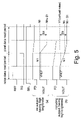
- FIG. 5 is a timing chart showing read operation of a pixel signal in each of pixels of an image sensor
- FIG. 6 is a circuit diagram showing a reference voltage generator according to a second embodiment of the imaging device of the present invention.
- FIG. 7 is a circuit diagram showing a reference voltage generator according to a third embodiment of the imaging device of the present invention.
- FIG. 8 is a circuit diagram showing a reference voltage generator according to a fourth embodiment of the imaging device of the present invention.
- FIG. 9 is a block diagram showing the details of a pixel array according to the fourth embodiment.
- each bold line represents a signal line consisting of a plurality of lines. Some of blocks connected with the bold line consist of a plurality of circuits, respectively. Signal lines for transmitting signals are designated by the same reference symbols as the names of the signals.
- FIG. 1 shows a first embodiment of an imaging device according to the present invention.
- This imaging device is formed as a CMOS image sensor chip on a silicon substrate using CMOS technology.
- the imaging device includes a constant voltage generator 10 , an operation control circuit 12 , a reference voltage generator 14 , a noise voltage switching circuit 16 , a correlated double sampling circuit (CDS circuit) 18 , and a pixel array ARY.
- CDS circuit correlated double sampling circuit
- the constant voltage generator 10 generates an internal voltage VR which is constant at all times, according to a power supply voltage AVDD.
- the power supply voltage AVDD is the power supply voltage for analog circuits.
- a power supply voltage DVDD for digital circuits may be supplied to the constant voltage generator 10 .
- the internal voltage VR is the voltage lower than the power supply voltage AVDD, and is kept constant at all times irrespective of the change in the power supply voltage AVDD and the change in temperature.
- the operation control circuit 12 controls the operation of the imaging device as a whole.
- the operation control circuit 12 outputs a reset signal RST, a transfer control signal TG, and a selection control signal SEL to the pixel array ARY, and outputs a standby signal XPD to the reference voltage generator 14 .
- the standby signal XPD changes to a high level during an operation period (light-receiving operation) when pixels PX detect light, and changes to a low level during a standby period when the pixels PX do not detect light.
- the reference voltage generator 14 generates a reference voltage (second reference voltage) VREF, according to the internal voltage VR.
- the reference voltage generator 14 generates the reference voltage VREF while it receives the high-level standby signal XPD, and stops generating the reference voltage VREF while it receives the low-level standby signal XPD.
- the noise voltage switching circuit 16 When a voltage level VOUT (noise voltage, noise data) of a read signal exceeds the reference voltage VREF during a reset period of read operation which will be described later, the noise voltage switching circuit 16 outputs this voltage level VOUT as a noise voltage VOUT 1 .
- the noise voltage switching circuit 16 When the voltage level VOUT of the read signal is equal to or lower than the reference voltage VREF during the reset period, the noise voltage switching circuit 16 outputs a fixed first voltage V 1 as the noise voltage VOUT 1 .
- the first voltage V 1 shows a standard level (black level) when brightness of a subject is zero, for example.
- the CDS circuit 18 subtracts the noise data (noise voltage) read during the reset period from pixel data (pixel voltage) read during the read period, generates true pixel data without including the noise, and outputs the generated pixel data as a pixel signal SIG.
- the pixel array ARY includes a plurality of the pixels PX arranged in a matrix state. The pixel data and the noise data obtained by photoelectric conversion by the respective pixels PX are outputted as a detection voltage VOUT.
- FIG. 2 shows the details of the pixel array ARY shown in FIG. 1 .
- the pixel PX of this embodiment is the so-called 4-transistor type.
- Each pixel PX includes nMOS transistors M 1 , M 2 and a photodiode PD (photoelectric conversion circuit) which are connected in series between an internal voltage line VR and a ground line VSS, and nMOS transistors M 3 , M 4 and a current source CS 1 which are connected in series between the internal voltage line VR and the ground line VSS.
- a source of the transistor M 4 is connected to a detection voltage line VOUT through which the read voltage and the noise voltage are outputted.
- a gate of the transistor M 1 receives the reset signal RST.
- a gate of the transistor M 2 receives the transfer control signal TG.
- a gate of the transistor M 3 (source follower transistor) is connected to a connecting node FD (floating diffusion node) between the transistors M 1 and M 2 .
- a gate of the transistor M 4 (selection transistor) receives the selection control signal SEL.
- the transistor M 3 is the source follower transistor.
- the transistors M 3 and M 4 constitute a source follower circuit SF 1 (first source follower circuit).
- FIG. 3 shows the details of the reference voltage generator 14 shown in FIG. 1 .
- the reference voltage generator 14 includes a voltage generator VG, a source follower circuit SF 2 (second source follower circuit) having the same electric characteristics as the source follower circuit SF 1 of the pixel PX, a current source CS 2 , and an amplifier AMP.
- the voltage generator VG includes resistors R 1 , R 2 and R 3 which are connected in series between the internal voltage line VR and the ground line VSS, and switches SW 1 and SW 2 which connect connecting nodes between the resistors R 1 to R 3 to a gate of an nMOS transistor M 5 of the source follower circuit SF 2 .
- Either of the switches SW 1 and SW 2 turns on according to a value of a resister formed inside the image sensor.
- the value of the resister is set by a user (system) using the image sensor when turning the power on, for example.
- the switches SW 1 and SW 2 By switching between the switches SW 1 and SW 2 , either of two voltages generated by a resistor row R 1 to R 3 is supplied as a first reference voltage VR 1 to the gate of the transistor M 5 of the source follower circuit SF 2 .
- the gate voltage of the transistor M 5 is set slightly lower than the noise voltage when the pixels PX do not receive light. Since the gate voltage of the transistor M 5 can be switched by the switches SW 1 and SW 2 , it is possible to ship an image sensor chip as the image sensor for a plurality of specifications (characteristics), for example.
- the source follower circuit SF 2 includes nMOS transistors M 5 and M 6 whose threshold values are the same as the nMOS transistors M 3 and M 4 of the source follower circuit SF 1 , respectively.
- gate widths of the transistors M 5 and M 6 are respectively designed to be twice as large as gate widths of the transistors M 3 and M 4 .
- Channel lengths of the transistors M 5 and M 6 are the same as channel lengths of the transistors M 3 and M 4 .
- a current amount flowing in the source follower circuit SF 2 can be made larger as compared to the source follower circuit SF 1 . Accordingly, it is possible for the source follower circuit SF 2 to operate stably and generate the stable second reference voltage with high accuracy.
- a current amount of the current source CS 2 is also designed to be twice as large as a current amount of the current source CS 1 .
- a gate of the transistor M 6 receives the standby signal XPD. Since the transistor M 6 is turned off during the standby period when the pixels PX do not detect light, it is possible to reduce a standby current.
- the current source CS 2 is arranged between a source of the transistor M 6 and the ground line VSS.
- the amplifier AMP amplifies a source voltage of the transistor M 6 and outputs it as the reference voltage VREF.
- the source follower circuit SF 2 which is the same as that of the pixel PX is formed inside the reference voltage generator 14 . Accordingly, when fabricating conditions of the image sensor vary in its fabrication process and the threshold voltages of the transistors (M 3 and M 4 , for example) inside the pixel PX change, the reference voltage VREF also changes. More specifically, when the threshold voltages of the transistors M 3 and M 4 in the pixel PX are high, the noise voltage decreases relatively. Since the image sensor is formed by one chip, the threshold voltages of the transistors M 5 and M 6 increase along with the threshold voltages of the transistors M 3 and M 4 . Therefore, the reference voltage VREF decreases following the noise voltage.
- the noise voltage switching circuit 16 shown in FIG. 4 operates stably.
- FIG. 4 shows the details of the noise voltage switching circuit 16 shown in FIG. 1 .
- the noise voltage switching circuit 16 includes a decision circuit DC which compares the reference voltage VREF and the noise voltage VOUT outputted from the pixels PX, and switches SW 3 and SW 4 which turn on/off according to the decision result of the decision circuit DC.
- the decision circuit DC outputs a high level when the noise voltage VOUT is higher than the reference voltage VREF. In this case, the switch SW 3 turns off and the switch SW 4 turns on.
- the CDS circuit 18 generates the pixel signal SIG using the noise voltage VOUT read from the pixels PX. Meanwhile, the decision circuit DC outputs a low level when the noise voltage VOUT is equal to or lower than the reference voltage VREF. In this case, the switch SW 3 turns on and the switch SW 4 turns off.
- the CDS circuit 18 generates the pixel signal SIG using the fixed first voltage V 1 .
- FIG. 5 shows the read operation of the pixel signal in each of the pixels of the image sensor described above.
- the read operation is made of a noise data read period and a pixel data read period.
- the selection control signal SEL is set at the high level (power supply voltage) in order to turn on the transistor M 4 .
- the reset signal RST and the transfer control signal TG are set at the low level (ground voltage) in order to turn off the transistors M 1 and M 2 .
- the reset signal RST is changed to the high level, and the transistor M 1 is turned on.
- the node FD is reset to the internal voltage VR.
- the reset signal RST is changed to the low level, and noise data N 1 is read. Since the source follower circuit SF 1 is operated accompanying the change in the voltage of the node FD, the noise data (noise voltage) N 1 is outputted as the detection voltage VOUT.
- the transfer control signal TG is changed to the high level, and the transistor M 2 is turned on.
- the transistor M 2 By turning on the transistor M 2 , electric charges accumulated in the photodiode by capturing the image of the subject are transferred to the node FD.
- the voltage of the node FD decreases according to the amount of the charges.
- the change in the voltage of the node FD is also influenced by the noise data N 1 .
- the transfer control signal TG is changed to the low level, and the pixel data including the noise data N 1 (N 1 +S 1 ) is read. Since the source follower circuit SF 1 is operated accompanying the change in the voltage of the node FD, the pixel data (pixel voltage) including the noise data N 1 is outputted as the detection voltage VOUT.
- the CDS circuit 18 shown in FIG. 1 subtracts the noise voltage N 1 from the pixel voltage including the noise data N 1 (N 1 +S 1 ), and outputs the true pixel data excluding the noise data as the pixel signal SIG.
- the noise voltage N 1 is higher than the reference voltage VREF. Therefore, the correct noise data N 1 is read during the noise data read period.
- the noise voltage switching circuit 16 shown in FIG. 4 turns off the switch SW 3 and turns on the switch SW 4 , to output the noise voltage N 1 to the CDS circuit 18 .
- the noise voltage N 1 becomes lower than the reference voltage VREF due to the leakage of the electric charges caused in a substrate and so on of the image sensor.
- the noise voltage switching circuit 16 turns on the switch SW 3 and turns off the switch SW 4 , to output the fixed first voltage V 1 showing the virtual noise to the CDS circuit 18 .
- the reference voltage generator 14 includes the source follower circuit SF 2 having the same electric characteristics as the source follower circuit SF 1 formed in the pixel PX. Accordingly, when the fabricating conditions in semiconductor fabrication process vary and the threshold voltages of the transistors constituting the image sensor change, the reference voltage VREF also changes following the change in the noise voltage N 1 . Therefore, in a reset state of the pixel PX (period when the reset signal RST is at the high level), the noise voltage N 1 is higher than the reference voltage VREF by a predetermined value at all times, irrespective of the threshold voltages of the transistors. The noise voltage N 1 in the reset state varies depending on the threshold voltages of the transistors.
- the above-mentioned predetermined value has varied between plural image sensors formed on a wafer, wafers, and lots.
- the present invention it is possible to allow a difference between the noise voltage V 1 and the reference voltage VREF in the reset state to be constant at all times between the plural image sensors on the wafer, the wafers, and the lots.
- the noise voltage N 1 it is possible to prevent the noise voltage N 1 from being too high as compared to the reference voltage VREF, and to solve the problem that the noise voltage N 1 cannot be switched to the first voltage V 1 although the phenomenon of black sun is occurring.
- the reference voltage generator 14 includes the source follower circuit SF 2 whose threshold voltages are the same as those of the source follower circuit SF 1 in the pixel PX. Therefore, even when the threshold voltages of the transistors constituting the image sensor change due to the variation of the fabricating conditions, it is possible to change the reference voltage VREF following the change in the noise voltage N 1 in the reset state. Since a desired reference voltage VREF can be generated according to the electric characteristics of the source follower circuit SF 1 inside the pixel PX, the noise voltage switching circuit 16 can be operated normally at all times. As a result of this, it is possible to prevent the phenomenon of the black sun without fail, and to prevent the image quality from deteriorating when the subject having high brightness is captured.
- a trimming circuit (fuse circuit) or the like for selecting any one of the plural reference voltages according to the electric characteristics of the formed transistor becomes unnecessary.
- a passivation layer of the chip in the periphery of the fuse circuit needs to be eliminated in order to perform laser cutting in test process, and the process of selectively eliminating the passivation layer is necessary in the fabrication process.
- the electric characteristics of the image sensor are evaluated, and the fuse is cut according to the evaluation result.
- the present invention it is possible to prevent the fabrication process of the image sensor from increasing and to eliminate the test process for the trimming. It is also possible to eliminate the equipment such as a testing apparatus. Further, since the fuse circuit becomes unnecessary, chip size can be reduced. As a result of this, it is possible to reduce fabrication cost of the image sensor.
- the gate widths of the transistors of the source follower circuit SF 2 are larger than the gate widths of the transistors of the source follower circuit SF 1 , the current amount flowing in the source follower circuit SF 2 can be increased. As a result of this, it is possible for the source follower circuit SF 2 to generate the stable reference voltage VREF with high accuracy.
- the voltage generator VG of the reference voltage generator 14 selects any one of the plural voltages by the switches SW 1 and SW 2 , and outputs is as the first reference voltage VR 1 (gate voltage of the transistor M 5 ). Therefore, it is possible to ship an image sensor chip as the image sensor for a plurality of specifications (characteristics), and to reduce developing cost of the image sensor.
- FIG. 6 shows a reference voltage generator 14 A according to a second embodiment of the imaging device of the present invention.
- the reference voltage generator 14 A is formed instead of the reference voltage generator 14 of the first embodiment.
- its structure is the same as that of the first embodiment. That is, this imaging device is formed as a CMOS image sensor chip on a silicon substrate using CMOS technology.
- the reference voltage generator 14 A includes a constant voltage generator 20 instead of the voltage generator VG in the reference voltage generator 14 of the first embodiment. In other respects, its structure is the same as that of the reference voltage generator 14 .
- the constant voltage generator 20 generates a constant voltage CV 1 which is constant at all times, in response to a power supply voltage AVDD.
- the constant voltage CV 1 is lower than an internal voltage VR, and is kept constant at all times irrespective of the change in the power supply voltage AVDD and the change in temperature.
- a power supply voltage DVDD for digital circuits may be supplied to the constant voltage generator 20 .
- a gate voltage to be supplied to a transistor M 5 in a source follower circuit SF 2 can be made constant at all times. Accordingly, a reference voltage VREF changes in response to only the variation of threshold voltages of transistors constituting the source follower circuit SF 2 .
- the reference voltage REF can be made constant irrespective of the change in the power supply voltage and change in the temperature, and can be changed following only the change in a noise voltage N 1 in a reset state (that is, the difference of the threshold voltages of the transistors constituting the source follower circuit SF 1 ) without fail.
- FIG. 7 shows a reference voltage generator 14 B according to a third embodiment of the imaging device of the present invention.
- the reference voltage generator 14 B is formed instead of the reference voltage generator 14 of the first embodiment.
- its structure is the same as that of the first embodiment. That is, this imaging device is formed as a CMOS image sensor chip on a silicon substrate using CMOS technology.
- the reference voltage generator 14 B includes a constant voltage generator 20 together with the voltage generator VG in the reference voltage generator 14 of the first embodiment. In other respects, its structure is the same as that of the reference voltage generator 14 .
- An output CV 1 of the constant voltage generator 20 is connected to a gate of a transistor M 5 in a source follower circuit SF 2 via a switch SW 5 . Any one of switches SW 1 , SW 2 and SW 5 turns on according to a value of a resister formed inside the image sensor. The value of the resister is set by a user (system) using the image sensor when turning the power on, for example. Whichever switch is turned on among the switches SW 1 , SW 2 and SW 5 , the gate voltage of the transistor M 5 is set slightly lower than a noise voltage when pixels PX do not receive light.
- any one of three kinds of voltages can be selected by the switch SW 1 , SW 2 or SW 5 , and outputted as a first reference voltage VR 1 (gate voltage of the transistor M 5 ). Therefore, it is possible to form the image sensor for many more specifications (characteristics) using an image sensor chip, and to reduce the developing cost of the image sensor.
- FIG. 8 shows a reference voltage generator 14 C according to a fourth embodiment of the imaging device of the present invention.
- the reference voltage generator 14 C is formed instead of the reference voltage generator 14 of the first embodiment.
- its structure is the same as that of the first embodiment. That is, this imaging device is formed as a CMOS image sensor chip on a silicon substrate using CMOS technology.
- the reference voltage generator 14 C includes a pair of source follower circuits SF 3 (second source follower circuits) arranged in parallel between a voltage generator VG and an amplifier AMP.
- Each of the source follower circuits SF 3 includes nMOS transistors M 7 and M 8 whose threshold voltages are the same as the nMOS transistors M 3 and M 4 of the source follower circuit SF 1 , respectively.
- gate widths of the transistors M 7 and M 8 are the same as gate widths of the transistors M 3 and M 4 .
- Channel lengths of the transistors M 7 and M 8 are the same as channel lengths of the transistors M 3 and M 4 .
- the plural source follower circuits SF 3 in the reference voltage generator 14 C have the same effect as the increase of the gate widths of the transistors in one source follower circuit (SF 1 in the first embodiment, for example). That is, similarly to the first embodiment, it is possible to increase a current amount flowing in the source follower circuits SF 3 and to operate the source follower circuits SF 3 stably.
- FIG. 9 shows the details of a pixel array ARY according to the fourth embodiment.
- the pixel array ARY includes a plurality of pixels PX arranged in a matrix state. Dummy pixels DPX formed in a dummy region DMY positioned on an outermost side of the pixel array ARY are not used for photoelectric conversion. The dummy pixels DPX are formed to form the inner pixels PX to have the ideal shape.
- source follower areas SFA are formed inside the dummy region DMY.
- the source follower circuits SF 3 shown in FIG. 8 are formed by using the source follower circuits SF 1 which are formed in the pixels PX in the source follower areas SFA. Especially, the source follower circuits SF 3 of this embodiment are formed by using the pixels PX which are shown in half-tone dot meshing and are positioned diagonally in the pixel array ARY.
- the source follower circuits SF 3 are formed at the positions separated from each other in the pixel array ARY, so that the average characteristics of the source follower circuit SF 3 can be obtained without fail.
- a pair of the source follower circuits SF 3 are dispersively arranged inside the pixel array ARY, so that the characteristics of the source follower circuits SF 3 can be averaged. Accordingly, the reference voltage generator 14 C can generate the average reference voltage VREF independent of individual circuit characteristics of the source follower circuit SF 3 . Further, since the total amount of the current flowing in the source follower circuits SF 3 can be increased, it is possible for the reference voltage generator 14 C to generate the stable reference voltage VREF with high accuracy.
- the source follower circuits SF 3 are formed by using the source follower circuits SF 1 of the pixels PX formed in the dummy region DMY in the pixel array ARY. Therefore, the electric characteristics of the source follower circuits SF 3 are easily brought into agreement with those of the source follower circuits SF 1 . Further, the source follower circuits SF 3 are respectively formed by using the pixels PX in the source follower areas SFA formed on both right and left sides of the pixel array ARY. Since the source follower circuits SF 3 are formed at the positions separated from each other in the pixel array ARY, the average reference voltage VREF can be generated with ease.
- the above-described first and second embodiment have dealt with the case where the gate widths of the transistors M 5 and M 6 of the source follower circuit SF 2 are designed to be twice as large as the gate widths of the transistors M 3 and M 4 of the source follower circuit SF 1 .
- the present invention is not limited to such embodiments.
- the transistors M 5 and M 6 may be designed to have the identical size with the transistors M 3 and M 4 .
- the source follower circuit SF 2 may be constituted by using the source follower circuit SF 1 of the pixel PX formed in the dummy region in the pixel array ARY or the like. By forming the source follower circuit SF 2 inside the pixel array ARY, it is possible to equalize the electric characteristics of the source follower circuits SF 1 and SF 2 without fail.
- the above-described fourth embodiment has dealt with the case where a pair of the source follower circuits SF 3 are formed using the pixels PX which are positioned diagonally in the pixel array ARY.
- the number of the source follower circuits SF 3 may be larger than two.
- the four source follower circuits SF 3 may be formed by using the pixels PX positioned at four corners of the pixel array ARY.
Landscapes
- Engineering & Computer Science (AREA)
- Multimedia (AREA)
- Signal Processing (AREA)
- Power Engineering (AREA)
- Transforming Light Signals Into Electric Signals (AREA)
- Solid State Image Pick-Up Elements (AREA)
Abstract
Description
Claims (15)
Applications Claiming Priority (2)
| Application Number | Priority Date | Filing Date | Title |
|---|---|---|---|
| JP2005-027771 | 2005-02-03 | ||
| JP2005027771A JP4425809B2 (en) | 2005-02-03 | 2005-02-03 | Imaging device |
Publications (2)
| Publication Number | Publication Date |
|---|---|
| US20060170794A1 US20060170794A1 (en) | 2006-08-03 |
| US7477299B2 true US7477299B2 (en) | 2009-01-13 |
Family
ID=36756087
Family Applications (1)
| Application Number | Title | Priority Date | Filing Date |
|---|---|---|---|
| US11/133,386 Expired - Fee Related US7477299B2 (en) | 2005-02-03 | 2005-05-20 | Imaging device |
Country Status (4)
| Country | Link |
|---|---|
| US (1) | US7477299B2 (en) |
| JP (1) | JP4425809B2 (en) |
| KR (1) | KR100732140B1 (en) |
| CN (1) | CN1816113B (en) |
Cited By (5)
| Publication number | Priority date | Publication date | Assignee | Title |
|---|---|---|---|---|
| US20070291147A1 (en) * | 2006-06-12 | 2007-12-20 | Daisuke Muraoka | Photoelectric conversion device, image sensor, optical reader, and method of driving photoelectric conversion device |
| US20100053379A1 (en) * | 2007-05-21 | 2010-03-04 | Trygve Willassen | Suppression of Row-Wise Noise in CMOS Image Sensors |
| US20110141324A1 (en) * | 2006-08-31 | 2011-06-16 | Sony Corporation | Solid-state image sensor and image capturing apparatus |
| US8773191B2 (en) | 2012-09-07 | 2014-07-08 | Samsung Electronics Co., Ltd. | Analog-to-digital conversion circuit, and image sensor including the same |
| US10096632B2 (en) | 2016-02-11 | 2018-10-09 | Samsung Electronics Co., Ltd. | Image sensor |
Families Citing this family (22)
| Publication number | Priority date | Publication date | Assignee | Title |
|---|---|---|---|---|
| JP4720508B2 (en) * | 2006-01-05 | 2011-07-13 | 株式会社ニコン | Imaging device and imaging apparatus |
| JP4305507B2 (en) * | 2006-12-18 | 2009-07-29 | ソニー株式会社 | Imaging device and camera |
| JP2008199254A (en) * | 2007-02-13 | 2008-08-28 | Matsushita Electric Ind Co Ltd | Solid-state imaging device, driving method thereof, and imaging device |
| US20080204567A1 (en) * | 2007-02-23 | 2008-08-28 | Weize Xu | Sample and hold circuits with buffer offset removed |
| FR2914499B1 (en) * | 2007-04-02 | 2009-05-29 | St Microelectronics Sa | METHOD AND CIRCUIT FOR OBTAINING A SAMPLE IN AN IMAGE SENSOR |
| JP5256711B2 (en) * | 2007-11-28 | 2013-08-07 | 株式会社ニコン | Imaging device and imaging apparatus |
| JP5108713B2 (en) * | 2008-10-10 | 2012-12-26 | パナソニック株式会社 | Solid-state imaging device and imaging device |
| JP5511203B2 (en) * | 2009-03-16 | 2014-06-04 | キヤノン株式会社 | Imaging device and imaging apparatus |
| US20120211642A1 (en) * | 2009-10-27 | 2012-08-23 | Konica Minolta Opto, Inc. | Solid-State Imaging Device |
| CN102213614B (en) * | 2010-04-09 | 2013-05-01 | 中国科学院微电子研究所 | Method for eliminating imaging device process mismatch and imaging nonlinear influence |
| JP5473775B2 (en) * | 2010-05-18 | 2014-04-16 | キヤノン株式会社 | Imaging device |
| JP5810493B2 (en) | 2010-09-03 | 2015-11-11 | ソニー株式会社 | Semiconductor integrated circuit, electronic equipment, solid-state imaging device, imaging device |
| TWI504259B (en) * | 2011-01-03 | 2015-10-11 | Himax Imaging Inc | Dark compensation circuit |
| CN102625057B (en) * | 2011-01-26 | 2015-03-11 | 英属开曼群岛商恒景科技股份有限公司 | Dark sun compensating circuit |
| CN102196201B (en) * | 2011-06-23 | 2013-11-27 | 格科微电子(上海)有限公司 | Signal readout circuit, module and method of image sensor |
| US9274152B2 (en) * | 2013-01-30 | 2016-03-01 | Atmel Corporation | Current-based charge compensation in a touch sensor |
| CN105338268B (en) | 2014-08-12 | 2018-09-11 | 比亚迪股份有限公司 | Imaging sensor and its removal solar spot method and removal solar spot device |
| EP3358828A4 (en) * | 2015-10-02 | 2019-03-13 | Olympus Corporation | IMAGE CAPTURE ELEMENT AND ENDOSCOPE |
| CN108063905B (en) * | 2016-11-09 | 2020-04-14 | 京东方科技集团股份有限公司 | Pixel sensing circuit and driving method thereof, image sensor, electronic device |
| US10721427B2 (en) * | 2018-06-25 | 2020-07-21 | Primesensor Technology Inc. | Image sensor circuit and ramp signal generator thereof |
| CN112119629A (en) * | 2019-07-31 | 2020-12-22 | 深圳市大疆创新科技有限公司 | Image sensor and method and device for acquiring pixel information |
| KR102740392B1 (en) * | 2020-12-24 | 2024-12-06 | 엘지디스플레이 주식회사 | Array substrate for digital x-ray detector and the digital x-ray detector including the same |
Citations (19)
| Publication number | Priority date | Publication date | Assignee | Title |
|---|---|---|---|---|
| JPH0965215A (en) | 1995-08-29 | 1997-03-07 | Olympus Optical Co Ltd | Solid-state image pickup device |
| US6166767A (en) * | 1996-12-10 | 2000-12-26 | Sharp Kabushiki Kaisha | Active solid-state imaging device which effectively suppresses fixed-pattern noise |
| US6201572B1 (en) * | 1998-02-02 | 2001-03-13 | Agilent Technologies, Inc. | Analog current mode assisted differential to single-ended read-out channel operable with an active pixel sensor |
| US20010013901A1 (en) * | 1995-08-11 | 2001-08-16 | Yoshiyuki Matsunaga | MOS-type solid-state imaging apparatus |
| US20010052941A1 (en) * | 1995-08-11 | 2001-12-20 | Yoshiyuki Matsunaga | Image system, solid-state imaging semiconductor integrated circuit device used in the image system, and difference output method used for the image system |
| US20020012057A1 (en) * | 2000-05-26 | 2002-01-31 | Hajime Kimura | MOS sensor and drive method thereof |
| US20030025817A1 (en) * | 1996-10-17 | 2003-02-06 | Kazuya Yonemoto | Solid state imaging device, signal processing method and driving method therefor and camera |
| US20040046879A1 (en) * | 1985-11-15 | 2004-03-11 | Cannon Kabushiki Kaisha | Solid state image pickup apparatus |
| JP2004112740A (en) | 2002-07-25 | 2004-04-08 | Fujitsu Ltd | Image sensor with improved image quality |
| US6798452B1 (en) * | 1997-07-28 | 2004-09-28 | Matsushita Electric Industrial Co., Ltd. | Amplifying solid-state imaging device, method for driving the same and physical quantity distribution sensing semiconductor device |
| US20050068432A1 (en) * | 1997-10-06 | 2005-03-31 | Canon Kabushiki Kaisha | Image sensor and method for driving an image sensor for reducing fixed pattern noise |
| US20050195306A1 (en) * | 2004-03-04 | 2005-09-08 | Sharp Kabushiki Kaisha | Solid-state image pickup device |
| US20050206764A1 (en) * | 1998-02-20 | 2005-09-22 | Canon Kabushiki Kaisha | Photoelectric converter and radiation reader |
| US6963367B1 (en) * | 1999-07-08 | 2005-11-08 | Canon Kabushiki Kaisha | Image pickup apparatus |
| US7098950B2 (en) * | 2000-03-28 | 2006-08-29 | Fujitsu Limited | Image sensor with stabilized black level and low power consumption |
| US20080057615A1 (en) * | 2006-08-31 | 2008-03-06 | Canon Kabushiki Kaisha | Manufacturing method of photoelectric conversion device |
| US7375753B2 (en) * | 2002-02-12 | 2008-05-20 | Sony Corporation | Solid-state imager and camera system |
| US7382409B2 (en) * | 2003-03-27 | 2008-06-03 | Canon Kabushiki Kaisha | Image pickup apparatus including circuitry to correct for noise generated by clamping circuits |
| US7408577B2 (en) * | 2003-04-09 | 2008-08-05 | Micron Technology, Inc. | Biasing scheme for large format CMOS active pixel sensors |
Family Cites Families (4)
| Publication number | Priority date | Publication date | Assignee | Title |
|---|---|---|---|---|
| US4819070A (en) * | 1987-04-10 | 1989-04-04 | Texas Instruments Incorporated | Image sensor array |
| US6194696B1 (en) * | 1998-03-10 | 2001-02-27 | Photobit Corporation | Active pixel sensor with current mode readout |
| KR19990086296A (en) * | 1998-05-27 | 1999-12-15 | 윤종용 | Screen output inspection and adjustment device of video display and method |
| US6753912B1 (en) * | 1999-08-31 | 2004-06-22 | Taiwan Advanced Sensors Corporation | Self compensating correlated double sampling circuit |
-
2005
- 2005-02-03 JP JP2005027771A patent/JP4425809B2/en not_active Expired - Fee Related
- 2005-05-19 KR KR1020050042017A patent/KR100732140B1/en not_active Expired - Fee Related
- 2005-05-20 US US11/133,386 patent/US7477299B2/en not_active Expired - Fee Related
- 2005-06-13 CN CN2005100766914A patent/CN1816113B/en not_active Expired - Fee Related
Patent Citations (20)
| Publication number | Priority date | Publication date | Assignee | Title |
|---|---|---|---|---|
| US20040046879A1 (en) * | 1985-11-15 | 2004-03-11 | Cannon Kabushiki Kaisha | Solid state image pickup apparatus |
| US20010013901A1 (en) * | 1995-08-11 | 2001-08-16 | Yoshiyuki Matsunaga | MOS-type solid-state imaging apparatus |
| US20010052941A1 (en) * | 1995-08-11 | 2001-12-20 | Yoshiyuki Matsunaga | Image system, solid-state imaging semiconductor integrated circuit device used in the image system, and difference output method used for the image system |
| US20020149688A9 (en) * | 1995-08-11 | 2002-10-17 | Yoshiyuki Matsunaga | MOS-type solid-state imaging apparatus |
| JPH0965215A (en) | 1995-08-29 | 1997-03-07 | Olympus Optical Co Ltd | Solid-state image pickup device |
| US20030025817A1 (en) * | 1996-10-17 | 2003-02-06 | Kazuya Yonemoto | Solid state imaging device, signal processing method and driving method therefor and camera |
| US6166767A (en) * | 1996-12-10 | 2000-12-26 | Sharp Kabushiki Kaisha | Active solid-state imaging device which effectively suppresses fixed-pattern noise |
| US6798452B1 (en) * | 1997-07-28 | 2004-09-28 | Matsushita Electric Industrial Co., Ltd. | Amplifying solid-state imaging device, method for driving the same and physical quantity distribution sensing semiconductor device |
| US20050068432A1 (en) * | 1997-10-06 | 2005-03-31 | Canon Kabushiki Kaisha | Image sensor and method for driving an image sensor for reducing fixed pattern noise |
| US6201572B1 (en) * | 1998-02-02 | 2001-03-13 | Agilent Technologies, Inc. | Analog current mode assisted differential to single-ended read-out channel operable with an active pixel sensor |
| US20050206764A1 (en) * | 1998-02-20 | 2005-09-22 | Canon Kabushiki Kaisha | Photoelectric converter and radiation reader |
| US6963367B1 (en) * | 1999-07-08 | 2005-11-08 | Canon Kabushiki Kaisha | Image pickup apparatus |
| US7098950B2 (en) * | 2000-03-28 | 2006-08-29 | Fujitsu Limited | Image sensor with stabilized black level and low power consumption |
| US20020012057A1 (en) * | 2000-05-26 | 2002-01-31 | Hajime Kimura | MOS sensor and drive method thereof |
| US7375753B2 (en) * | 2002-02-12 | 2008-05-20 | Sony Corporation | Solid-state imager and camera system |
| JP2004112740A (en) | 2002-07-25 | 2004-04-08 | Fujitsu Ltd | Image sensor with improved image quality |
| US7382409B2 (en) * | 2003-03-27 | 2008-06-03 | Canon Kabushiki Kaisha | Image pickup apparatus including circuitry to correct for noise generated by clamping circuits |
| US7408577B2 (en) * | 2003-04-09 | 2008-08-05 | Micron Technology, Inc. | Biasing scheme for large format CMOS active pixel sensors |
| US20050195306A1 (en) * | 2004-03-04 | 2005-09-08 | Sharp Kabushiki Kaisha | Solid-state image pickup device |
| US20080057615A1 (en) * | 2006-08-31 | 2008-03-06 | Canon Kabushiki Kaisha | Manufacturing method of photoelectric conversion device |
Cited By (9)
| Publication number | Priority date | Publication date | Assignee | Title |
|---|---|---|---|---|
| US20070291147A1 (en) * | 2006-06-12 | 2007-12-20 | Daisuke Muraoka | Photoelectric conversion device, image sensor, optical reader, and method of driving photoelectric conversion device |
| US7626628B2 (en) * | 2006-06-12 | 2009-12-01 | Daisuke Muraoka | Photoelectric conversion device, image sensor, optical reader, and method of driving photoelectric conversion device |
| US20110141324A1 (en) * | 2006-08-31 | 2011-06-16 | Sony Corporation | Solid-state image sensor and image capturing apparatus |
| US8421888B2 (en) * | 2006-08-31 | 2013-04-16 | Sony Corporation | Solid state imaging device having signal noise combining circuitry for masking image reproduction errors |
| US20100053379A1 (en) * | 2007-05-21 | 2010-03-04 | Trygve Willassen | Suppression of Row-Wise Noise in CMOS Image Sensors |
| US8310569B2 (en) * | 2007-05-21 | 2012-11-13 | Aptina Imaging Corporation | Suppression of row-wise noise in CMOS image sensors |
| US8773191B2 (en) | 2012-09-07 | 2014-07-08 | Samsung Electronics Co., Ltd. | Analog-to-digital conversion circuit, and image sensor including the same |
| US9282264B2 (en) | 2012-09-07 | 2016-03-08 | Samsung Electronics Co., Ltd. | Analog-to-digital conversion circuit, and image sensor including the same |
| US10096632B2 (en) | 2016-02-11 | 2018-10-09 | Samsung Electronics Co., Ltd. | Image sensor |
Also Published As
| Publication number | Publication date |
|---|---|
| CN1816113A (en) | 2006-08-09 |
| KR100732140B1 (en) | 2007-06-27 |
| KR20060090147A (en) | 2006-08-10 |
| JP2006217244A (en) | 2006-08-17 |
| CN1816113B (en) | 2010-06-02 |
| US20060170794A1 (en) | 2006-08-03 |
| JP4425809B2 (en) | 2010-03-03 |
Similar Documents
| Publication | Publication Date | Title |
|---|---|---|
| US7477299B2 (en) | Imaging device | |
| US9288416B2 (en) | Reference voltage circuit and image-capture circuit | |
| CN102037722B (en) | Solid-state imaging device, imaging device, and pixel driving method | |
| US11330214B2 (en) | Comparator and image sensing device including the same | |
| US10917595B2 (en) | Image sensor and output compensation circuit of image sensor | |
| EP2150038B1 (en) | Image sensor pixel with gain control | |
| KR101696410B1 (en) | Image sensor and method of operating the same | |
| JP5631555B2 (en) | Image sensor and readout system thereof | |
| WO2008088879A1 (en) | Image sensor with gain control | |
| US10958858B2 (en) | Ramp signal generator and image sensor including the same | |
| US10771723B2 (en) | Systems and methods for voltage settling | |
| US20040195491A1 (en) | Signal processing circuit, image sensor IC, and signal processing method | |
| US20050035273A1 (en) | Photoelectric converter and a method of driving the same | |
| US7501609B2 (en) | Image sensor with linearly mounted image sensor IC's | |
| WO2007099850A1 (en) | Solid-state image sensor and solid-state image sensor signal generation method | |
| CN113228623A (en) | Ultra-high dynamic range CMOS sensor | |
| JP4654046B2 (en) | Clamp circuit for CMOS image sensor | |
| JP4935227B2 (en) | Temperature detection circuit, operation method thereof, and semiconductor device | |
| US7679663B2 (en) | Photodetection apparatus | |
| US9762839B2 (en) | Image capturing apparatus, image capturing system, and method for driving image capturing apparatus | |
| US8648950B2 (en) | Image sensor for minimizing variation of control signal level | |
| JP3527911B2 (en) | Optical sensor monitor circuit | |
| CN115209069A (en) | Image sensing device | |
| EP1874044B1 (en) | Solid state imaging device |
Legal Events
| Date | Code | Title | Description |
|---|---|---|---|
| AS | Assignment |
Owner name: FUJITSU LIMITED, JAPAN Free format text: ASSIGNMENT OF ASSIGNORS INTEREST;ASSIGNORS:HIGUCHI, TSUYOSHI;FUNAKOSHI, JUN;YAMAGATA, SEIJI;AND OTHERS;REEL/FRAME:016591/0390 Effective date: 20050425 |
|
| AS | Assignment |
Owner name: FUJITSU MICROELECTRONICS LIMITED, JAPAN Free format text: ASSIGNMENT OF ASSIGNORS INTEREST;ASSIGNOR:FUJITSU LIMITED;REEL/FRAME:021977/0219 Effective date: 20081104 Owner name: FUJITSU MICROELECTRONICS LIMITED,JAPAN Free format text: ASSIGNMENT OF ASSIGNORS INTEREST;ASSIGNOR:FUJITSU LIMITED;REEL/FRAME:021977/0219 Effective date: 20081104 |
|
| AS | Assignment |
Owner name: FUJITSU SEMICONDUCTOR LIMITED, JAPAN Free format text: CHANGE OF NAME;ASSIGNOR:FUJITSU MICROELECTRONICS LIMITED;REEL/FRAME:024982/0245 Effective date: 20100401 |
|
| FPAY | Fee payment |
Year of fee payment: 4 |
|
| AS | Assignment |
Owner name: SOCIONEXT INC., JAPAN Free format text: ASSIGNMENT OF ASSIGNORS INTEREST;ASSIGNOR:FUJITSU SEMICONDUCTOR LIMITED;REEL/FRAME:035508/0469 Effective date: 20150302 |
|
| REMI | Maintenance fee reminder mailed | ||
| LAPS | Lapse for failure to pay maintenance fees | ||
| STCH | Information on status: patent discontinuation |
Free format text: PATENT EXPIRED DUE TO NONPAYMENT OF MAINTENANCE FEES UNDER 37 CFR 1.362 |
|
| STCH | Information on status: patent discontinuation |
Free format text: PATENT EXPIRED DUE TO NONPAYMENT OF MAINTENANCE FEES UNDER 37 CFR 1.362 |
|
| FP | Lapsed due to failure to pay maintenance fee |
Effective date: 20170113 |