US7451368B2 - Semiconductor device and method for testing semiconductor device - Google Patents
Semiconductor device and method for testing semiconductor device Download PDFInfo
- Publication number
- US7451368B2 US7451368B2 US10/951,398 US95139804A US7451368B2 US 7451368 B2 US7451368 B2 US 7451368B2 US 95139804 A US95139804 A US 95139804A US 7451368 B2 US7451368 B2 US 7451368B2
- Authority
- US
- United States
- Prior art keywords
- circuit
- logic
- data
- memory
- semiconductor device
- Prior art date
- Legal status (The legal status is an assumption and is not a legal conclusion. Google has not performed a legal analysis and makes no representation as to the accuracy of the status listed.)
- Expired - Fee Related, expires
Links
Images


Classifications
-
- G—PHYSICS
- G11—INFORMATION STORAGE
- G11C—STATIC STORES
- G11C29/00—Checking stores for correct operation ; Subsequent repair; Testing stores during standby or offline operation
- G11C29/04—Detection or location of defective memory elements, e.g. cell constructio details, timing of test signals
- G11C29/08—Functional testing, e.g. testing during refresh, power-on self testing [POST] or distributed testing
- G11C29/12—Built-in arrangements for testing, e.g. built-in self testing [BIST] or interconnection details
- G11C29/1201—Built-in arrangements for testing, e.g. built-in self testing [BIST] or interconnection details comprising I/O circuitry
-
- G—PHYSICS
- G11—INFORMATION STORAGE
- G11C—STATIC STORES
- G11C29/00—Checking stores for correct operation ; Subsequent repair; Testing stores during standby or offline operation
- G11C29/04—Detection or location of defective memory elements, e.g. cell constructio details, timing of test signals
- G11C29/08—Functional testing, e.g. testing during refresh, power-on self testing [POST] or distributed testing
- G11C29/12—Built-in arrangements for testing, e.g. built-in self testing [BIST] or interconnection details
- G11C29/36—Data generation devices, e.g. data inverters
-
- G—PHYSICS
- G11—INFORMATION STORAGE
- G11C—STATIC STORES
- G11C29/00—Checking stores for correct operation ; Subsequent repair; Testing stores during standby or offline operation
- G11C29/04—Detection or location of defective memory elements, e.g. cell constructio details, timing of test signals
- G11C2029/0401—Detection or location of defective memory elements, e.g. cell constructio details, timing of test signals in embedded memories
-
- G—PHYSICS
- G11—INFORMATION STORAGE
- G11C—STATIC STORES
- G11C29/00—Checking stores for correct operation ; Subsequent repair; Testing stores during standby or offline operation
- G11C29/04—Detection or location of defective memory elements, e.g. cell constructio details, timing of test signals
- G11C29/08—Functional testing, e.g. testing during refresh, power-on self testing [POST] or distributed testing
- G11C29/12—Built-in arrangements for testing, e.g. built-in self testing [BIST] or interconnection details
- G11C29/36—Data generation devices, e.g. data inverters
- G11C2029/3602—Pattern generator
-
- G—PHYSICS
- G11—INFORMATION STORAGE
- G11C—STATIC STORES
- G11C29/00—Checking stores for correct operation ; Subsequent repair; Testing stores during standby or offline operation
- G11C29/56—External testing equipment for static stores, e.g. automatic test equipment [ATE]; Interfaces therefor
- G11C2029/5602—Interface to device under test
Definitions
- the present invention relates to a semiconductor device in which a plurality of semiconductor chips are mounted in a single package, or to a so-called multi-chip package (MCP), and to a method for testing such a semiconductor device.
- MCP multi-chip package
- Japanese Laid-Open Patent Publication No. 2003-77296 describes a conventional semiconductor device.
- the semiconductor device is a single package including a logic chip (logic LSI) provided with a data processing function and a memory chip (memory LSI) for storing data that has been or will be processed by the logic chip.
- the logic chip includes a digital signal processor (DSP).
- DSP digital signal processor
- the logic circuit processes predetermined data provided to the DSP and provides the processed data to the memory chip.
- the data is written to or stored in a memory circuit, such as a flash memory included in the memory chip. Further, the data processed by the logic circuit may be written beforehand to the memory circuit.
- a semiconductor device having such a configuration reduces the package cost.
- any combination of the LSIs mounted in the package may be selected. This reduces the risks and costs for developing a system LSI.
- An MCP including a logic chip and a memory chip normally includes many terminal pins.
- a memory tester capable of testing only packages having a small number of terminal pins cannot be used to test an MCP.
- a logic tester capable of testing an MCP having many terminal pins is used.
- a typical logic tester generates test signals that are more complicated than those generated by a memory tester and makes determinations based on the test signals.
- the logic tester may be applied to a package having many terminals pins, the number of packages that may be simultaneously tested is small.
- a memory chip in an MCP is an electrically rewritable non-volatile memory such as a flash memory
- the time required to write data to the memory chip is long. Accordingly, the testing cost is high when conducting tests with a logic tester that can simultaneously test only a small number of packages.
- One aspect of the present invention is a semiconductor device having a plurality of packaged semiconductor chips.
- the semiconductor chips include a logic chip, provided with a logic circuit for processing data, and a memory chip, provided with an electrically rewriteable non-volatile memory circuit for storing data that is processed by or that is to be processed by the logic circuit.
- An automatic rewrite circuit automatically writes test data to the memory circuit in accordance with a command signal from an external device.
- a switch circuit connected to the automatic rewrite circuit and the logic circuit switches between accessing of the memory circuit by the automatic rewrite circuit and accessing of the memory circuit by the logic circuit.
- the semiconductor chips include a logic chip, provided with a logic circuit for processing data, and a memory chip, provided with an electrically rewriteable non-volatile memory circuit for storing data that is processed by or that is to be processed by the logic circuit.
- the semiconductor device includes an automatic rewrite circuit, for automatically writing test data to the memory circuit in accordance with a command signal from an external device, and a switch circuit, for switching between accessing of the memory circuit by the automatic rewrite circuit and accessing of the memory circuit by the logic circuit.
- the method includes automatically writing test data to the memory circuit with the automatic rewrite circuit, and testing the operation of the logic circuit with the external device, with the testing being performed in parallel to said automatically writing test data.
- a further aspect of the present invention is a method for testing a semiconductor device having a plurality of packaged semiconductor chips.
- the semiconductor chips include a logic chip, provided with a logic circuit for processing data, and a memory chip, provided with an electrically rewriteable non-volatile memory circuit for storing data that is processed by or that is to be processed by the logic circuit.
- the method includes automatically writing test data to the memory circuit in accordance with a command signal from an external device by using an automatic rewrite circuit, and switching between accessing of the memory circuit by the automatic rewrite circuit and accessing of the memory circuit by the logic circuit.
- FIG. 1 is a schematic block diagram of a semiconductor device according to a first embodiment of the present invention
- FIG. 2 is a detailed block diagram of the semiconductor device of the first embodiment
- FIG. 3 is a flowchart showing the procedures for testing the semiconductor device of the first embodiment
- FIG. 4 is a schematic block diagram showing a semiconductor device according to a second embodiment of the present invention.
- FIG. 5 is a table showing commands for rewriting data to and reading data from a flash memory
- FIG. 6 is a timing chart showing an erase operation for the flash memory.
- FIG. 7 is a timing chart showing a program operation for the flash memory.
- a semiconductor device and a method for testing the semiconductor device according to a first embodiment of the present invention will now be described.
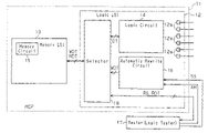
- the semiconductor device 11 includes a plurality of semiconductor chips and is a so-called multi-chip package (MCP).
- the semiconductor chips mounted on the semiconductor device 11 includes a logic chip 12 (logic LSI), which is provided with a function for processing data, and a memory chip 13 (memory LSI), which stores the data processed by the logic chip 12 or data to be processed by the logic chip 12 .
- logic LSI logic LSI
- memory LSI memory LSI
- the logic chip 12 includes a logic circuit 14 , such as a digital signal processor (DSP).
- the logic circuit 14 processes data provided through terminals 12 a (only some are shown for the sake of convenience) of the logic chip 12 .
- the processed data DT is normally provided to the memory chip 13 and written to a memory circuit 15 , which is incorporated in the memory chip 13 .
- data DT that is pre-written to the memory circuit 15 is processed by the logic circuit 14 and output to external devices via the terminals 12 a .
- the memory circuit 15 is a flash memory circuit.
- the logic chip 12 includes an automatic rewrite circuit 16 that automatically tests operations for rewriting data, such as the erasing (deleting) of data from the memory circuit 15 and the programming (writing) of data to the memory circuit 15 .
- the rewrite operation testing of the memory circuit 15 is performed when the logic circuit 14 is tested. That is, the rewrite operation testing is performed independently from and parallel to the testing of the logic circuit 14 .
- the three operations of erasing (deleting), programming (writing), and reading are performed on the memory circuit 15 .
- the speed of the erasing operation and the speed of the programming operation are slow. Accordingly, in the present embodiment, the testing of the data rewrite operation in which data is erased from and programmed in the memory circuit 15 is performed parallel to the testing of the logic circuit.
- most of the data rewrite testing for the memory circuit 15 is performed parallel to the testing of the logic circuit 14 . This shortens the test period.
- the operation speed for reading data from the memory circuit 15 is relatively fast. Thus, even if operation testing is performed separately in the memory circuit 15 and the logic circuit 14 , this would not delay the testing of the MCP semiconductor device 11 as a whole. Further, a determination circuit, which is required for a typical built-in automatic testing circuit, is eliminated from the automatic rewrite circuit 16 that is mounted on the logic chip 12 even though such a determination circuit would not cause delays in testing of the memory circuit 15 . This reduces the circuit scale of the automatic rewrite circuit 16 and satisfies the demand for a more compact semiconductor device.
- FIGS. 5 to 7 show a typical command system and the process timing of a flash memory. Referring to FIG. 5 , before the flash memory performs deleting, rewriting, or reading, the flash memory is provided with a few cycles of commands configured by predetermined addresses and data.
- delete command addresses and command data are sequentially input. Then, the delete operation is started in accordance with the delete address (sector address) and data 30 h (refer to FIG. 5 ) input in the sixth bus cycle.
- the delete command addresses and command data serve as a delete signal.
- write command addresses and command data for four bus cycles are sequentially input. Then, the write operation is started in accordance with the write address and write data input in the fourth bus cycle.
- the write command addresses and command data serve as a write signal.
- the automatic rewrite circuit 16 is provided with a test start command SS and an operation mode setting signal AM (e.g., signal having several bits) from an external device, or logic tester 17 , which also tests the logic circuit 14 .
- the automatic rewrite circuit 16 starts testing the data rewrite operation.
- the operation mode setting signal AM includes information related with operation modes, such as the program operation and the erase operation, and information related with data patterns (e.g., full board program and checkerboard program) during program operation.
- the tester 17 provides the memory chip 13 with a data read command RS.
- the tester 17 retrieves data RDT, which is read from the memory circuit 15 .
- a determination circuit which is incorporated in the tester 17 , determines the results of the test from the data RDT.
- a selector 18 in the logic chip 12 switches between accessing by the tester 17 , accessing of the memory chip 13 (memory circuit 15 ) by the automatic rewrite circuit 16 , and normal accessing of the logic circuit 14 . Since the automatic rewrite circuit 16 and the selector 18 are both incorporated in the logic chip 12 , the configuration of the memory chip 13 does not have to be changed.
- the automatic rewrite circuit 16 will now be described with reference to FIG. 2 .
- the automatic rewrite circuit 16 includes a rewrite control circuit 16 a , a counter circuit 16 b , an address generation circuit 16 c , a data pattern generation circuit 16 d , and a programming/erase command generation circuit 16 e .
- the rewrite control circuit 16 a generates a rewrite control signal for every predetermined cycle in accordance with the test command signal SS, which is provided from the tester 17 .
- the counter circuit 16 b performs a count operation in synchronism with the rewrite control signal.
- the address generation circuit 16 c generates a rewrite address in accordance with a count value of the counter circuit 16 b .
- the data pattern generation circuit 16 d generates rewrite data in accordance with the operation mode setting signal AM.
- the programming/erase command generation circuit 16 e generates a programming/erase command in accordance with the operation mode setting signal AM.
- the rewrite control signal, the rewrite address, the rewrite data, and the programming/erase command are provided to the memory chip 13 via the selector 18 .
- data is rewritten to the memory circuit 15 according to these signals and commands in the modes described below.
- the rewrite control signal for example, a chip enable signal CE#, an output enable signal OE#, or a write enable signal WE#, is provided to the control logic 13 b via a control signal input circuit 13 a.
- the programming/erase command generation circuit 16 e generates the programming/erase command as two signals, a command address signal and a command data signal.
- the command address signal is provided to an address buffer-latch 13 d via an address input circuit 13 c of the memory chip 13 , latched by the address buffer-latch 13 d , and then provided to the control logic 13 b .
- the command data signal is provided to an input/output buffer-data latch 13 f via a data input/output circuit 13 e of the memory chip 13 and then provided to the control logic 13 b.
- the address generation circuit 16 c provides the generated rewrite address to the control logic 13 b , a row decoder 13 g , and a column decoder 13 h via the address input circuit 13 c and the address buffer-latch 13 d .
- the data pattern generation circuit 16 d provides the generated rewrite data to the control logic 13 b and the column decoder 13 h via the data input/output circuit 13 e and the input/output buffer-data latch 13 f.
- the control logic 13 b determines whether to enter the programming operation or the erase operation based on the programming/erase command, or the combination of the command address and the command data signal, and sets the operation mode in accordance with the determination.
- the rewrite control circuit 16 a In accordance with the programming or erase operation mode, the rewrite control circuit 16 a generates the rewrite control signal for the next rewrite address after the time required for rewriting data to the memory circuit 15 elapses.
- the control logic 13 b is electrically connected to a voltage adjustment circuit (not shown). The voltage adjustment circuit adjusts the voltage applied to the memory circuit 15 in accordance with a control signal provided from the control logic 13 b.
- the rewrite control circuit 16 a After data is rewritten to the entire memory cell, the rewrite control circuit 16 a does not automatically output the rewrite control signal. Thus, the output timing of the rewrite control signal is changed in accordance with the memory capacity of the memory circuit 15 . Further, the address generation circuit 16 c changes the method for generating an address in accordance with the operation mode setting signal AM. For example, when erasing a sector, an address incremented by the number of addresses corresponding to a sector unit is generated. When writing data in a checkerboard pattern, an address is incremented by two. Subsequently, in the modes described below, the rewritten test data is read and a determination is made based on the test result.
- the tester 17 outputs a read control signal and a read address as the read command RS.
- the read control signal is provided to the control logic 13 b via the control signal input circuit 13 a of the memory chip 13 .
- the read address is provided to the address buffer-latch 13 d via the address input circuit 13 c of the memory chip 13 and latched by the address buffer-latch 13 d .
- the read address is then provided to the control logic 13 b , the row decoder 13 g , and the column decoder 13 h.
- the memory circuit 15 reads test data from a memory cell that corresponds to the read address provided to the decoders 13 g and 13 h .
- the read test data is provided to the input/output buffer-data latch 13 f via the column decoder 13 h , latched by the input/output buffer-data latch 13 f , and output to the memory chip 13 via the data input/output circuit 13 e .
- the test data is retrieved by the tester 17 via the selector 18 .
- the tester 17 determines whether the memory chip 13 is functioning properly based on the test data. More specifically, the tester 17 includes an expected data pattern generation circuit for generating data used to determine proper functioning in synchronism with the read control signal. The proper functioning determination data is generated through a measurement program, which is generated in accordance with the data written to the memory circuit 15 . The tester 17 compares the read test data with the proper functioning determination data to determine whether or not the memory chip 13 is functioning properly.
- step S 1 the tester 17 outputs the test start command SS and the operation mode setting signal AM to the automatic rewrite circuit 16 .
- steps S 2 to S 4 the tester 17 executes a series of tests on the logic circuit 14 .
- the automatic rewrite circuit 16 starts to automatically rewrite data to the memory circuit 15 in step S 5 .
- step S 6 the automatic rewrite circuit 16 ends the rewriting of data to the memory circuit 15 .
- the tester 17 repetitively performs the processes of steps S 1 to S 7 until completing the testing of the logic circuit 14 or the testing of the memory circuit 15 (step S 8 ).
- the logic chip 12 of the semiconductor device includes the automatic rewrite circuit 16 , which automatically rewrites data to the memory circuit 15 .
- the rewriting of data to the memory circuit 15 is performed independently from and in parallel to the testing of the logic circuit 14 .
- a semiconductor package that has a simple configuration and includes a plurality of semiconductor chips is tested efficiently, and the time for testing the semiconductor device is reduced.
- the scale of the automatic rewrite circuit 16 is small. This does not contradict with the demand for a more compact semiconductor device.
- the automatic rewrite circuit 16 is incorporated in the logic chip 12 .
- the circuit configuration of the memory chip 13 does not have to be changed even when the automatic rewrite circuit 16 is employed.
- a semiconductor device 21 and a method for testing the semiconductor device 21 according to a second embodiment of the present invention will now be described with reference to FIG. 4 .
- the semiconductor device 21 is an MCP including a plurality of packaged semiconductor chips.
- the semiconductor chips mounted on the semiconductor device 11 includes a logic chip 22 (logic LSI), which is provided with a function for processing data, and a memory chip 23 (memory LSI), which stores the data processed by the logic chip 12 or data to be processed by the logic chip 12 .
- the logic chip 22 includes a logic circuit 24 , such as a digital signal processor (DSP).
- the logic circuit 14 processes data provided through terminals 22 a of the logic chip 22 .
- the processed data DT is normally provided to the memory chip 23 and written to a memory circuit 25 , which is incorporated in the memory chip 23 .
- data DT that is processed by the logic circuit 14 may be pre-written to the memory circuit 15 .
- the data processed by the logic circuit 24 is output to external devices via the terminals 22 a .
- the memory circuit 25 is, for example, a flash memory circuit.
- the memory chip 23 includes an automatic rewrite circuit 26 that automatically rewrites data to the memory circuit 25 . Accordingly, a selector 28 in the memory chip 23 switches between accessing by a tester 27 , accessing of the memory circuit 25 by the automatic rewrite circuit 26 , and normal accessing of the logic circuit 14 .
- the rewriting of data to the memory circuit 25 may also be performed during the time the logic circuit 24 is tested. That is, the rewriting of data to the memory circuit 25 may be performed in parallel to and independently from the testing of the logic circuit 24 . Thus, the semiconductor device is tested efficiently. This reduces the entire testing time.
- the automatic rewrite circuit 26 starts the rewriting of data when receiving a test start command SS and an operation mode setting signal AM from an external device, or the logic tester 27 , which also tests the logic circuit 24 .
- the automatic rewrite circuit 26 differs from the first embodiment in that the rewriting of data to the memory circuit 25 by the automatic rewrite circuit 26 ends when the memory chip 23 outputs a completion signal ED to the tester 27 .
- the tester 27 recognizes the completion of data rewriting by the automatic rewrite circuit 26 , the tester 27 accesses the memory chip 23 , reads and retrieves the test data stored in the memory circuit 25 , and determines whether the test data is proper with an incorporated determination circuit.
- the configuration and operation of the automatic rewrite circuit 26 is substantially the same as in the first embodiment.
- the second embodiment differs from the first embodiment in that the control logic 13 b outputs the rewrite completion signal ED to the tester 27 when the final rewrite address is input and the rewriting of that data is completed.
- the second embodiment has advantages (1) and (3) of the first embodiment.
- the second embodiment also has an advantage similar to advantage (2) of the first embodiment.
- the automatic rewrite circuit 26 is incorporated in the memory chip 23 .
- the circuit configuration of the logic chip 22 does not have to be changed even when the automatic rewrite circuit 26 is employed.
- the memory circuits 15 and 25 are not limited to flash memories and may be an electrically rewriteable non-volatile memory, such as an EEPROM.
Abstract
Description
Claims (5)
Applications Claiming Priority (2)
| Application Number | Priority Date | Filing Date | Title |
|---|---|---|---|
| JP2003-340192 | 2003-09-30 | ||
| JP2003340192A JP4248359B2 (en) | 2003-09-30 | 2003-09-30 | Semiconductor device and test method thereof |
Publications (2)
| Publication Number | Publication Date |
|---|---|
| US20050068818A1 US20050068818A1 (en) | 2005-03-31 |
| US7451368B2 true US7451368B2 (en) | 2008-11-11 |
Family
ID=34373391
Family Applications (1)
| Application Number | Title | Priority Date | Filing Date |
|---|---|---|---|
| US10/951,398 Expired - Fee Related US7451368B2 (en) | 2003-09-30 | 2004-09-28 | Semiconductor device and method for testing semiconductor device |
Country Status (5)
| Country | Link |
|---|---|
| US (1) | US7451368B2 (en) |
| JP (1) | JP4248359B2 (en) |
| KR (1) | KR100632338B1 (en) |
| CN (1) | CN100468578C (en) |
| TW (1) | TWI249171B (en) |
Cited By (2)
| Publication number | Priority date | Publication date | Assignee | Title |
|---|---|---|---|---|
| US20090054022A1 (en) * | 2007-08-21 | 2009-02-26 | Sanyo Electric Co., Ltd. | Semiconductor device for use in radio tuner and method for manufacturing the same |
| US20090063792A1 (en) * | 2007-09-05 | 2009-03-05 | Nec Electronics Corporation | Memory control circuit, semiconductor integrated circuit, and verification method of nonvolatile memory |
Families Citing this family (2)
| Publication number | Priority date | Publication date | Assignee | Title |
|---|---|---|---|---|
| JP2007335809A (en) * | 2006-06-19 | 2007-12-27 | Nec Electronics Corp | Semiconductor device and method for controlling operation of semiconductor device |
| US8259521B2 (en) * | 2008-05-28 | 2012-09-04 | Macronix International Co., Ltd. | Method and circuit for testing a multi-chip package |
Citations (5)
| Publication number | Priority date | Publication date | Assignee | Title |
|---|---|---|---|---|
| US4931997A (en) * | 1987-03-16 | 1990-06-05 | Hitachi Ltd. | Semiconductor memory having storage buffer to save control data during bulk erase |
| US6006313A (en) * | 1995-06-19 | 1999-12-21 | Sharp Kabushiki Kaisha | Semiconductor memory device that allows for reconfiguration around defective zones in a memory array |
| US6009547A (en) * | 1997-12-03 | 1999-12-28 | International Business Machines Corporation | ECC in memory arrays having subsequent insertion of content |
| US20030043612A1 (en) | 2001-09-05 | 2003-03-06 | Fujitsu Limited | Semiconductor device whereon memory chip and logic chip are mounted, making testing of memory chip possible |
| US6708302B1 (en) * | 1999-12-10 | 2004-03-16 | Renesas Technology Corp. | Semiconductor module |
-
2003
- 2003-09-30 JP JP2003340192A patent/JP4248359B2/en not_active Expired - Fee Related
-
2004
- 2004-07-23 CN CNB2004100713768A patent/CN100468578C/en not_active Expired - Fee Related
- 2004-08-05 TW TW093123435A patent/TWI249171B/en not_active IP Right Cessation
- 2004-09-24 KR KR1020040077105A patent/KR100632338B1/en not_active IP Right Cessation
- 2004-09-28 US US10/951,398 patent/US7451368B2/en not_active Expired - Fee Related
Patent Citations (6)
| Publication number | Priority date | Publication date | Assignee | Title |
|---|---|---|---|---|
| US4931997A (en) * | 1987-03-16 | 1990-06-05 | Hitachi Ltd. | Semiconductor memory having storage buffer to save control data during bulk erase |
| US5084843A (en) * | 1987-03-16 | 1992-01-28 | Hitachi, Ltd. | Semiconductor memory having control means for preventing unauthorized erasure of a memory array portion |
| US6006313A (en) * | 1995-06-19 | 1999-12-21 | Sharp Kabushiki Kaisha | Semiconductor memory device that allows for reconfiguration around defective zones in a memory array |
| US6009547A (en) * | 1997-12-03 | 1999-12-28 | International Business Machines Corporation | ECC in memory arrays having subsequent insertion of content |
| US6708302B1 (en) * | 1999-12-10 | 2004-03-16 | Renesas Technology Corp. | Semiconductor module |
| US20030043612A1 (en) | 2001-09-05 | 2003-03-06 | Fujitsu Limited | Semiconductor device whereon memory chip and logic chip are mounted, making testing of memory chip possible |
Non-Patent Citations (1)
| Title |
|---|
| Patent Abstracts of Japan, Publication No. 2003-077296, Publication Date: Mar. 14, 2003, Title: "Semiconductor Device which Incorporates Memory Chip and Logic Chip, and in which Test of Memory Chip can be Performed". |
Cited By (3)
| Publication number | Priority date | Publication date | Assignee | Title |
|---|---|---|---|---|
| US20090054022A1 (en) * | 2007-08-21 | 2009-02-26 | Sanyo Electric Co., Ltd. | Semiconductor device for use in radio tuner and method for manufacturing the same |
| US20090063792A1 (en) * | 2007-09-05 | 2009-03-05 | Nec Electronics Corporation | Memory control circuit, semiconductor integrated circuit, and verification method of nonvolatile memory |
| US8117509B2 (en) * | 2007-09-05 | 2012-02-14 | Renesas Electronics Corporation | Memory control circuit, semiconductor integrated circuit, and verification method of nonvolatile memory |
Also Published As
| Publication number | Publication date |
|---|---|
| CN100468578C (en) | 2009-03-11 |
| TWI249171B (en) | 2006-02-11 |
| JP4248359B2 (en) | 2009-04-02 |
| JP2005106619A (en) | 2005-04-21 |
| KR20050031960A (en) | 2005-04-06 |
| KR100632338B1 (en) | 2006-10-11 |
| CN1604234A (en) | 2005-04-06 |
| US20050068818A1 (en) | 2005-03-31 |
| TW200523936A (en) | 2005-07-16 |
Similar Documents
| Publication | Publication Date | Title |
|---|---|---|
| US5825783A (en) | Semiconductor integrated circuit device with large-scale memory and controller embedded on one semiconductor chip and method of testing the device | |
| US7508724B2 (en) | Circuit and method for testing multi-device systems | |
| KR101075091B1 (en) | Semiconductor memory device and test method thereof | |
| KR100880517B1 (en) | Semiconductor memory and method for testing the same | |
| US6198663B1 (en) | Non-volatile semiconductor memory IC | |
| US8201037B2 (en) | Semiconductor integrated circuit and method for controlling semiconductor integrated circuit | |
| JP2000149588A5 (en) | ||
| US6639848B2 (en) | Semiconductor memory device and method for testing the same | |
| JP2004520673A (en) | Integrated circuit with embedded non-volatile memory self-diagnosis device and related diagnostic method | |
| US6930919B2 (en) | NAND-type flash memory device having array of status cells for storing block erase/program information | |
| US6724668B2 (en) | Semiconductor device provided with memory chips | |
| US20080282119A1 (en) | Memory device and built in self-test method of the same | |
| JP4939870B2 (en) | Semiconductor memory device and test method thereof | |
| US20060023544A1 (en) | Semiconductor device | |
| US4965768A (en) | Semiconductor device having programmable read only memory cells for specific mode | |
| JP2009099202A (en) | Semiconductor device | |
| US7451368B2 (en) | Semiconductor device and method for testing semiconductor device | |
| JP4882633B2 (en) | Memory test apparatus and memory test method | |
| JP2000163994A (en) | Semiconductor storage device | |
| US20030126525A1 (en) | Semiconductor device, method of testing the same and electronic instrument | |
| JP2003196999A (en) | Semiconductor integrated circuit test device and method | |
| KR20240032445A (en) | Semiconductor system including semiconductor device for performing defective analysis | |
| JP2001344999A (en) | Semiconductor device | |
| KR20090122874A (en) | Non volatile memory devicd and method of testing the same | |
| KR970029875A (en) | Confirmation method of erasing flash memory cell and its confirmation circuit |
Legal Events
| Date | Code | Title | Description |
|---|---|---|---|
| AS | Assignment |
Owner name: SANYO ELECTRIC CO., LTD., JAPAN Free format text: ASSIGNMENT OF ASSIGNORS INTEREST;ASSIGNORS:SHIBATA, SIGENORI;YOSHIKAWA, SADAO;WATANABE, TOMOFUMI;AND OTHERS;REEL/FRAME:015847/0689 Effective date: 20040922 |
|
| AS | Assignment |
Owner name: SANYO ELECTRIC CO., LTD., JAPAN Free format text: A CORRECTIVE ASSIGNMENT TO CORRECT THE ASSIGNOR ON REEL 015847 FRAME 0689;ASSIGNORS:SIBATA, SIGENORI;YOSHIKAWA, SADAO;WATANABE, TOMOFUMI;AND OTHERS;REEL/FRAME:016186/0977 Effective date: 20040922 |
|
| STCF | Information on status: patent grant |
Free format text: PATENTED CASE |
|
| FEPP | Fee payment procedure |
Free format text: PAYOR NUMBER ASSIGNED (ORIGINAL EVENT CODE: ASPN); ENTITY STATUS OF PATENT OWNER: LARGE ENTITY |
|
| CC | Certificate of correction | ||
| FEPP | Fee payment procedure |
Free format text: PAYOR NUMBER ASSIGNED (ORIGINAL EVENT CODE: ASPN); ENTITY STATUS OF PATENT OWNER: LARGE ENTITY Free format text: PAYER NUMBER DE-ASSIGNED (ORIGINAL EVENT CODE: RMPN); ENTITY STATUS OF PATENT OWNER: LARGE ENTITY |
|
| AS | Assignment |
Owner name: SEMICONDUCTOR COMPONENTS INDUSTRIES, LLC, ARIZONA Free format text: ASSIGNMENT OF ASSIGNORS INTEREST;ASSIGNOR:SANYO ELECTRIC CO., LTD.;REEL/FRAME:026594/0385 Effective date: 20110101 |
|
| FPAY | Fee payment |
Year of fee payment: 4 |
|
| AS | Assignment |
Owner name: SEMICONDUCTOR COMPONENTS INDUSTRIES, LLC, ARIZONA Free format text: CORRECTIVE ASSIGNMENT TO CORRECT THE INCORRECT #12/577882 PREVIOUSLY RECORDED ON REEL 026594 FRAME 0385. ASSIGNOR(S) HEREBY CONFIRMS THE ASSIGNMENT;ASSIGNOR:SANYO ELECTRIC CO., LTD;REEL/FRAME:032836/0342 Effective date: 20110101 |
|
| AS | Assignment |
Owner name: DEUTSCHE BANK AG NEW YORK BRANCH, NEW YORK Free format text: SECURITY INTEREST;ASSIGNOR:SEMICONDUCTOR COMPONENTS INDUSTRIES, LLC;REEL/FRAME:038620/0087 Effective date: 20160415 |
|
| FPAY | Fee payment |
Year of fee payment: 8 |
|
| AS | Assignment |
Owner name: DEUTSCHE BANK AG NEW YORK BRANCH, AS COLLATERAL AG Free format text: CORRECTIVE ASSIGNMENT TO CORRECT THE INCORRECT PATENT NUMBER 5859768 AND TO RECITE COLLATERAL AGENT ROLE OF RECEIVING PARTY IN THE SECURITY INTEREST PREVIOUSLY RECORDED ON REEL 038620 FRAME 0087. ASSIGNOR(S) HEREBY CONFIRMS THE SECURITY INTEREST;ASSIGNOR:SEMICONDUCTOR COMPONENTS INDUSTRIES, LLC;REEL/FRAME:039853/0001 Effective date: 20160415 Owner name: DEUTSCHE BANK AG NEW YORK BRANCH, AS COLLATERAL AGENT, NEW YORK Free format text: CORRECTIVE ASSIGNMENT TO CORRECT THE INCORRECT PATENT NUMBER 5859768 AND TO RECITE COLLATERAL AGENT ROLE OF RECEIVING PARTY IN THE SECURITY INTEREST PREVIOUSLY RECORDED ON REEL 038620 FRAME 0087. ASSIGNOR(S) HEREBY CONFIRMS THE SECURITY INTEREST;ASSIGNOR:SEMICONDUCTOR COMPONENTS INDUSTRIES, LLC;REEL/FRAME:039853/0001 Effective date: 20160415 |
|
| FEPP | Fee payment procedure |
Free format text: MAINTENANCE FEE REMINDER MAILED (ORIGINAL EVENT CODE: REM.); ENTITY STATUS OF PATENT OWNER: LARGE ENTITY |
|
| LAPS | Lapse for failure to pay maintenance fees |
Free format text: PATENT EXPIRED FOR FAILURE TO PAY MAINTENANCE FEES (ORIGINAL EVENT CODE: EXP.); ENTITY STATUS OF PATENT OWNER: LARGE ENTITY |
|
| STCH | Information on status: patent discontinuation |
Free format text: PATENT EXPIRED DUE TO NONPAYMENT OF MAINTENANCE FEES UNDER 37 CFR 1.362 |
|
| FP | Lapsed due to failure to pay maintenance fee |
Effective date: 20201111 |
|
| AS | Assignment |
Owner name: FAIRCHILD SEMICONDUCTOR CORPORATION, ARIZONA Free format text: RELEASE OF SECURITY INTEREST IN PATENTS RECORDED AT REEL 038620, FRAME 0087;ASSIGNOR:DEUTSCHE BANK AG NEW YORK BRANCH, AS COLLATERAL AGENT;REEL/FRAME:064070/0001 Effective date: 20230622 Owner name: SEMICONDUCTOR COMPONENTS INDUSTRIES, LLC, ARIZONA Free format text: RELEASE OF SECURITY INTEREST IN PATENTS RECORDED AT REEL 038620, FRAME 0087;ASSIGNOR:DEUTSCHE BANK AG NEW YORK BRANCH, AS COLLATERAL AGENT;REEL/FRAME:064070/0001 Effective date: 20230622 |