US7450074B2 - Mobile communication device - Google Patents
Mobile communication device Download PDFInfo
- Publication number
- US7450074B2 US7450074B2 US11/362,947 US36294706A US7450074B2 US 7450074 B2 US7450074 B2 US 7450074B2 US 36294706 A US36294706 A US 36294706A US 7450074 B2 US7450074 B2 US 7450074B2
- Authority
- US
- United States
- Prior art keywords
- mobile communication
- communication device
- node
- metal
- mhz
- Prior art date
- Legal status (The legal status is an assumption and is not a legal conclusion. Google has not performed a legal analysis and makes no representation as to the accuracy of the status listed.)
- Expired - Fee Related, expires
Links
- 238000010295 mobile communication Methods 0.000 title claims abstract description 45
- 239000002184 metal Substances 0.000 claims abstract description 81
- 238000002955 isolation Methods 0.000 claims description 8
- 239000000463 material Substances 0.000 claims description 2
- 238000005034 decoration Methods 0.000 claims 1
- 238000010586 diagram Methods 0.000 description 13
- MTLMVEWEYZFYTH-UHFFFAOYSA-N 1,3,5-trichloro-2-phenylbenzene Chemical compound ClC1=CC(Cl)=CC(Cl)=C1C1=CC=CC=C1 MTLMVEWEYZFYTH-UHFFFAOYSA-N 0.000 description 3
- 230000002452 interceptive effect Effects 0.000 description 2
- 238000012986 modification Methods 0.000 description 2
- 230000004048 modification Effects 0.000 description 2
- 230000001012 protector Effects 0.000 description 2
- 230000009977 dual effect Effects 0.000 description 1
- 230000005855 radiation Effects 0.000 description 1
Images


Classifications
-
- H—ELECTRICITY
- H01—ELECTRIC ELEMENTS
- H01Q—ANTENNAS, i.e. RADIO AERIALS
- H01Q1/00—Details of, or arrangements associated with, antennas
- H01Q1/12—Supports; Mounting means
- H01Q1/22—Supports; Mounting means by structural association with other equipment or articles
- H01Q1/24—Supports; Mounting means by structural association with other equipment or articles with receiving set
- H01Q1/241—Supports; Mounting means by structural association with other equipment or articles with receiving set used in mobile communications, e.g. GSM
- H01Q1/242—Supports; Mounting means by structural association with other equipment or articles with receiving set used in mobile communications, e.g. GSM specially adapted for hand-held use
- H01Q1/243—Supports; Mounting means by structural association with other equipment or articles with receiving set used in mobile communications, e.g. GSM specially adapted for hand-held use with built-in antennas
-
- H—ELECTRICITY
- H01—ELECTRIC ELEMENTS
- H01Q—ANTENNAS, i.e. RADIO AERIALS
- H01Q1/00—Details of, or arrangements associated with, antennas
- H01Q1/48—Earthing means; Earth screens; Counterpoises
Definitions
- the disclosure relates to a mobile communication device, and more particularly to a mobile communication device having a metal module.
- ESD electrostatic discharge
- a conventional solution increases elements in the mobile communication device to avoid the damage, however the cost of the mobile communication device is increased and usable space for electrical elements of the mobile communication device reduced.
- a conventional solution disposes a metal protector skirting the mobile communication device to increase rigidity.
- the metal protector interferes with the radiation of the mobile communication device, causing signal loss.
- Embodiments of the invention provide a mobile communication device comprising an antenna, a printed circuit board, and a metal module.
- the antenna transmits an output signal comprising a first resonance frequency and a wavelength.
- the printed circuit board comprises a metal grounding face and a layout face opposite the metal grounding face and is coupled to the antenna at a first node.
- the metal module is coupled to the metal grounding face at a second node.
- a distance between the first node and the second node is determined by the wavelength.
- FIG. 1 is a schematic diagram of a conventional mobile phone
- FIG. 2 is a schematic diagram of a cover of the mobile phone
- FIG. 3 is a connection schematic diagram of a metal module and PCB
- FIGS. 4 a ⁇ 4 c are return loss diagrams for the antenna
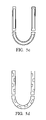
- FIGS. 5 a ⁇ 5 e are schematic diagrams of the metal module.
- Mobile communication devices for example personal digital assistants (PDA) and mobile phones, can be found in the market.
- PDA personal digital assistants
- a clam type mobile phone is given as an example of the mobile communication device, although the disclosure is not limited thereto.
- FIG. 1 is a schematic diagram of a clam type mobile phone 10 comprising a first section 11 , a second section 12 , a battery 13 , and an antenna 14 .
- Label 15 indicates the casing of first section 11 and label 16 indicates the casing of second section 12 .
- Antenna 14 transmits an output signal comprising a resonance frequency f and a wavelength ⁇ .
- C is light speed equal to 300,000,000.
- Antenna 14 is a spiral antenna transmitting dual frequencies of GSM and PCS/DCS type.
- Bandwidth of GSM is between 890 MHz and 960 MHz.
- Bandwidth of DCS is between 1710 MHz and 1880 MHz.
- Bandwidth of PCS is between 1850 MHz and 1990 MHz.
- FIG. 2 is a schematic diagram of the second section 12 comprising printed circuit board (PCB) 30 and metal module 40 .
- PCB 30 comprises a metal grounding face 32 , an isolation layer 34 , and a layout face 36 .
- Isolation layer 34 is disposed between metal grounding face 32 and layout face 36 .
- Material of isolation layer 34 is FR4.
- Layout face 36 is opposite to metal grounding face 32 .
- Antenna 14 is coupled to isolation layer 34 at node P 1 .
- metal grounding face 32 covers a part of isolation layer 34 , with antenna 14 coupled to another part of isolation layer 34 .
- Battery 13 is disposed on a surface of metal grounding face 32 providing power to PCB 30 .
- Metal module 40 surrounds PCB 30 and is coupled to PCB at at least one node (not shown). Since metal module 40 is coupled to metal grounding face 32 , when an ESD event occurs, discharge current generated thereby is quickly discharged to ground through metal grounding face 32 .
- FIG. 3 is a connection schematic diagram of metal module and PCB.
- metal module 40 is disposed in casing 16 .
- metal module 40 is disposed on an inner surface of casing 16 and coupled to metal grounding face 32 at nodes P 2 ⁇ P 5 .
- Metal module 40 can be disposed on an outer surface of casing 16 , but is not limited thereto.
- D 1 represents the distance between node P 2 and node P 1
- D 2 represents the distance between node P 3 and node P 1
- D 3 represents the distance between node P 4 and node P 1
- D 4 represents the distance between node P 5 and node P 1 .
- Distances D 1 ⁇ D 4 affect bandwidth and signal output of antenna 14 , thus distances D 1 ⁇ D 4 are determines by the wavelength ⁇ . For example, distances D 1 ⁇ D 4 may be determined by dividing the wavelength ⁇ .
- metal module 40 surrounds clam type mobile phone 10 , as clam type mobile phone 10 is thrown, metal module 40 can protect clam type mobile phone 10 .
- distances between node Pi and nodes P 2 ⁇ P 5 are determined by the wavelength ⁇ for avoiding metal module 40 interfering with the output signal from antenna 14 .
- metal module 40 is coupled to metal grounding face 32 at four nodes P 2 ⁇ P 5 .
- the wavelength ⁇ is 0.1666 meters or 16.66 centimeters.
- formula (2) can be obtained assuming the specific relation ship between distances D 1 ⁇ D 4 and the wavelength ⁇ .
- distances D 1 ⁇ D 4 may be determined by dividing the wavelength ⁇ .
- D 1 ⁇ D 4 n/ 8 ⁇ (2)
- the specific relation ship between distances D 1 ⁇ D 4 and the wavelength ⁇ can be set by any relation.
- the specific relation is a dividing relation.
- output signal of antenna 14 is interfered with by metal module 40 , wherein the first node is coupled to the metal module 40 and the metal grounding face 32 and the second node are coupled to antenna 14 and metal grounding face 32 .
- FIGS. 4 a ⁇ 4 c are return loss diagrams for antenna 14 .
- FIG. 4 a is a return loss diagram for the antenna when a distance between the node coupled to metal module 40 and metal grounding face 32 , and that coupled to antenna 14 and metal grounding face 32 is less than 1 ⁇ 8 ⁇ .
- a minimum return loss of clam type mobile phone 10 is approximately ⁇ 19.00 dB as the resonance frequency provided by antenna 14 is between 1710 MHz ⁇ 1990 MHz.
- FIG. 4 b is a return loss diagram for the antenna when a distance between the node coupled to metal module 40 and metal grounding face 32 , and that coupled to antenna 14 and metal grounding face 32 is less than 1 ⁇ 4 ⁇ and exceeds 1 ⁇ 2 ⁇ .
- a minimum return loss of clam type mobile phone 10 is approximately ⁇ 20.00 dB when the resonance frequency provided by antenna 14 is between 1710 MHz ⁇ 1990 MHz.
- FIG. 4 c is a return loss diagram for the antenna when the distance between the node coupled to metal module 40 and metal grounding face 32 , and that coupled to antenna 14 and metal grounding face 32 , is approximately 1 ⁇ 4 ⁇ .
- a minimum return loss of clam type mobile phone 10 is approximately ⁇ 30.00 dB when the resonance frequency provided by antenna 14 is between 1710 MHz ⁇ 1990 MHz.
- a return loss for clam type mobile phone 10 is reduced when a specific relation ship, such as 1 ⁇ 4′, exist between the distance between the node coupled to metal module 40 and metal grounding face 32 , and that coupled to antenna 14 and metal grounding face 32 , and the wavelength ⁇ .
- Metal module 40 is not limited and can be formed to any shape.
- metal module 40 is U-shaped metal module.
- FIGS. 5 a ⁇ 5 e are schematic diagrams of metal module 40 .
- metal module 40 comprises three metal units.
- metal module 40 comprises circle notches.
- metal module 40 comprises oblong notches.
- metal module 40 is a zigzagged.
- metal module 40 is I-shaped.
- the metal module can quickly discharge current to ground when ESD events occur in the mobile communication device.
- the metal module provides enhanced protection to the mobile communication device from impact.
- clam type mobile phone 10 has a minimum return loss when a distances between a first node, coupled to the metal module and a metal grounding face, and a second node, coupled to an antenna and the metal grounding face, is determined by a wavelength ⁇ .
Landscapes
- Engineering & Computer Science (AREA)
- Computer Networks & Wireless Communication (AREA)
- Support Of Aerials (AREA)
- Telephone Set Structure (AREA)
- Transceivers (AREA)
Abstract
Description
λ=C/f (1)
D 1 ˜D 4 =n/8λ (2)
Claims (20)
Applications Claiming Priority (2)
| Application Number | Priority Date | Filing Date | Title |
|---|---|---|---|
| TW094106223A TWI259741B (en) | 2005-03-02 | 2005-03-02 | Mobile communication device |
| TW94106223 | 2005-03-02 |
Publications (2)
| Publication Number | Publication Date |
|---|---|
| US20060197709A1 US20060197709A1 (en) | 2006-09-07 |
| US7450074B2 true US7450074B2 (en) | 2008-11-11 |
Family
ID=36943647
Family Applications (1)
| Application Number | Title | Priority Date | Filing Date |
|---|---|---|---|
| US11/362,947 Expired - Fee Related US7450074B2 (en) | 2005-03-02 | 2006-02-28 | Mobile communication device |
Country Status (2)
| Country | Link |
|---|---|
| US (1) | US7450074B2 (en) |
| TW (1) | TWI259741B (en) |
Families Citing this family (1)
| Publication number | Priority date | Publication date | Assignee | Title |
|---|---|---|---|---|
| TWI573322B (en) * | 2012-06-15 | 2017-03-01 | 群邁通訊股份有限公司 | Antenna assembly and wireless communication device employing same |
Citations (2)
| Publication number | Priority date | Publication date | Assignee | Title |
|---|---|---|---|---|
| US6252552B1 (en) * | 1999-01-05 | 2001-06-26 | Filtronic Lk Oy | Planar dual-frequency antenna and radio apparatus employing a planar antenna |
| US20050184915A1 (en) * | 2004-02-25 | 2005-08-25 | Control4 Corporation | System for remotely controlling an electrical switching device |
-
2005
- 2005-03-02 TW TW094106223A patent/TWI259741B/en not_active IP Right Cessation
-
2006
- 2006-02-28 US US11/362,947 patent/US7450074B2/en not_active Expired - Fee Related
Patent Citations (2)
| Publication number | Priority date | Publication date | Assignee | Title |
|---|---|---|---|---|
| US6252552B1 (en) * | 1999-01-05 | 2001-06-26 | Filtronic Lk Oy | Planar dual-frequency antenna and radio apparatus employing a planar antenna |
| US20050184915A1 (en) * | 2004-02-25 | 2005-08-25 | Control4 Corporation | System for remotely controlling an electrical switching device |
Also Published As
| Publication number | Publication date |
|---|---|
| TWI259741B (en) | 2006-08-01 |
| US20060197709A1 (en) | 2006-09-07 |
| TW200633598A (en) | 2006-09-16 |
Similar Documents
| Publication | Publication Date | Title |
|---|---|---|
| JP4408128B2 (en) | Mobile terminal device | |
| CN208597073U (en) | Electronic equipment | |
| KR101221225B1 (en) | Handheld electronic devices with isolated antennas | |
| US9819071B2 (en) | Antenna apparatus and method of making same | |
| TWI511372B (en) | Antenna with variable distributed capacitance | |
| KR100342510B1 (en) | Flip-type terminal with slim-type microstrip patch antenna for gps | |
| US7471249B2 (en) | EMC metal-plate antenna and a communication system using the same | |
| JP6139279B2 (en) | ANTENNA DEVICE AND ELECTRONIC DEVICE HAVING THE ANTENNA DEVICE | |
| US20170207517A1 (en) | Antenna for portable device | |
| US20120105292A1 (en) | Communication Device and Antenna Thereof | |
| JPWO2007046285A1 (en) | Antenna unit and communication device | |
| US20200127388A1 (en) | Antenna structure and electronic device | |
| US20160329625A1 (en) | Wireless communication device and antenna thereof | |
| US7697712B2 (en) | Speaker device for improving antenna property in a wireless portable terminal | |
| WO2022116705A1 (en) | Antenna apparatus and electronic device | |
| TW202203501A (en) | Mobile device | |
| US7511671B2 (en) | Portable wireless apparatus | |
| US7450074B2 (en) | Mobile communication device | |
| WO2007099859A1 (en) | Portable wireless device | |
| US20150091774A1 (en) | Mobile communication device | |
| WO2010073416A1 (en) | Portable wireless device | |
| JP2012065034A (en) | Portable terminal | |
| US20160164183A1 (en) | Wide band antenna | |
| JP2002141723A (en) | Mount structure for antenna | |
| JP3237943B2 (en) | transceiver |
Legal Events
| Date | Code | Title | Description |
|---|---|---|---|
| AS | Assignment |
Owner name: BENQ CORPORATION, TAIWAN Free format text: ASSIGNMENT OF ASSIGNORS INTEREST;ASSIGNOR:TUNG, HAO-CHUN;REEL/FRAME:017629/0363 Effective date: 20060220 |
|
| AS | Assignment |
Owner name: QISDA CORPORATION, TAIWAN Free format text: CHANGE OF NAME;ASSIGNOR:BENQ CORPORATION;REEL/FRAME:021575/0024 Effective date: 20070831 |
|
| STCF | Information on status: patent grant |
Free format text: PATENTED CASE |
|
| FPAY | Fee payment |
Year of fee payment: 4 |
|
| FPAY | Fee payment |
Year of fee payment: 8 |
|
| FEPP | Fee payment procedure |
Free format text: MAINTENANCE FEE REMINDER MAILED (ORIGINAL EVENT CODE: REM.); ENTITY STATUS OF PATENT OWNER: LARGE ENTITY |
|
| LAPS | Lapse for failure to pay maintenance fees |
Free format text: PATENT EXPIRED FOR FAILURE TO PAY MAINTENANCE FEES (ORIGINAL EVENT CODE: EXP.); ENTITY STATUS OF PATENT OWNER: LARGE ENTITY |
|
| STCH | Information on status: patent discontinuation |
Free format text: PATENT EXPIRED DUE TO NONPAYMENT OF MAINTENANCE FEES UNDER 37 CFR 1.362 |
|
| FP | Lapsed due to failure to pay maintenance fee |
Effective date: 20201111 |