US7433604B1 - Direct-detection optical differential 8-level phase shift keying (OD8PSK) for spectrally efficient transmission - Google Patents
Direct-detection optical differential 8-level phase shift keying (OD8PSK) for spectrally efficient transmission Download PDFInfo
- Publication number
- US7433604B1 US7433604B1 US11/168,154 US16815405A US7433604B1 US 7433604 B1 US7433604 B1 US 7433604B1 US 16815405 A US16815405 A US 16815405A US 7433604 B1 US7433604 B1 US 7433604B1
- Authority
- US
- United States
- Prior art keywords
- optical
- encoded
- differentially
- signal
- bit
- Prior art date
- Legal status (The legal status is an assumption and is not a legal conclusion. Google has not performed a legal analysis and makes no representation as to the accuracy of the status listed.)
- Active, expires
Links
Images


Classifications
-
- H—ELECTRICITY
- H04—ELECTRIC COMMUNICATION TECHNIQUE
- H04B—TRANSMISSION
- H04B10/00—Transmission systems employing electromagnetic waves other than radio-waves, e.g. infrared, visible or ultraviolet light, or employing corpuscular radiation, e.g. quantum communication
- H04B10/50—Transmitters
- H04B10/501—Structural aspects
- H04B10/503—Laser transmitters
- H04B10/505—Laser transmitters using external modulation
- H04B10/5051—Laser transmitters using external modulation using a series, i.e. cascade, combination of modulators
-
- H—ELECTRICITY
- H04—ELECTRIC COMMUNICATION TECHNIQUE
- H04B—TRANSMISSION
- H04B10/00—Transmission systems employing electromagnetic waves other than radio-waves, e.g. infrared, visible or ultraviolet light, or employing corpuscular radiation, e.g. quantum communication
- H04B10/50—Transmitters
- H04B10/501—Structural aspects
- H04B10/503—Laser transmitters
- H04B10/505—Laser transmitters using external modulation
- H04B10/5053—Laser transmitters using external modulation using a parallel, i.e. shunt, combination of modulators
-
- H—ELECTRICITY
- H04—ELECTRIC COMMUNICATION TECHNIQUE
- H04B—TRANSMISSION
- H04B10/00—Transmission systems employing electromagnetic waves other than radio-waves, e.g. infrared, visible or ultraviolet light, or employing corpuscular radiation, e.g. quantum communication
- H04B10/50—Transmitters
- H04B10/501—Structural aspects
- H04B10/503—Laser transmitters
- H04B10/505—Laser transmitters using external modulation
- H04B10/5055—Laser transmitters using external modulation using a pre-coder
-
- H—ELECTRICITY
- H04—ELECTRIC COMMUNICATION TECHNIQUE
- H04B—TRANSMISSION
- H04B10/00—Transmission systems employing electromagnetic waves other than radio-waves, e.g. infrared, visible or ultraviolet light, or employing corpuscular radiation, e.g. quantum communication
- H04B10/50—Transmitters
- H04B10/516—Details of coding or modulation
- H04B10/548—Phase or frequency modulation
- H04B10/556—Digital modulation, e.g. differential phase shift keying [DPSK] or frequency shift keying [FSK]
- H04B10/5561—Digital phase modulation
-
- H—ELECTRICITY
- H04—ELECTRIC COMMUNICATION TECHNIQUE
- H04B—TRANSMISSION
- H04B10/00—Transmission systems employing electromagnetic waves other than radio-waves, e.g. infrared, visible or ultraviolet light, or employing corpuscular radiation, e.g. quantum communication
- H04B10/60—Receivers
- H04B10/66—Non-coherent receivers, e.g. using direct detection
- H04B10/67—Optical arrangements in the receiver
- H04B10/676—Optical arrangements in the receiver for all-optical demodulation of the input optical signal
- H04B10/677—Optical arrangements in the receiver for all-optical demodulation of the input optical signal for differentially modulated signal, e.g. DPSK signals
Definitions
- the invention relates to generating, distributing, and detecting optical signals and in particular to systems, devices, apparatus, and methods of generating, distributing and detecting optical signals for transmission of data in ultra high capacity optical transmission mediums.
- Ultra high capacity optical transmission systems require high spectral efficiency due to finite bandwidth of optical fibers.
- High spectral efficiency not only leads to larger aggregate capacity but also provides better tolerance to chromatic dispersion and polarization-mode dispersion (PMD).
- PMD chromatic dispersion and polarization-mode dispersion
- Spectral efficiency of modulation formats can be increased by using multilevel modulation.
- a preference for spectral efficient transmission systems is direct detection to allow simple receiver structures free of local oscillators and polarization control.
- DQPSK Optical differential quadrature phase shift keying
- DQPSK is a digital modulation technique commonly used with cellular systems.
- Motorola's CyberSurfr cable modem uses DQPSK to carry data upstream from the subscriber's computer to the Internet on a narrower frequency band than standard QPSK. Narrower bands allow more upstream channels, so the CyberSurfr has additional noise-free channels to choose from when it's installed.
- High spectral efficiency not only leads to larger aggregate capacity, but also provides better tolerance to chromatic dispersion and polarization mode dispersion (PMD).
- Direct detection on the other hand, allows simple receiver structures free of local oscillators and polarization control. Significant increase in chromatic dispersion tolerance and robustness against fiber nonlinearities in optical DQPSK transmission have been demonstrated while allowing simple direct detection.
- an 8-level amplitude and phase-shift keying (8-APSK) with direct detection combines binary amplitude-shift keying and DQPSK.
- This approach is a straightforward combination of two well-known modulation formats, directly yielding three binary output data sequences identical to the three input data sequences.
- the apparatus, system and method of the present invention is a practical implementation of constant-intensity optical differential 8-level phase-shift keying (OD8PSK) with direct detection for high-capacity spectrally-efficient fiber-optic transmission.
- Electrical encoding and optical encoding/modulation schemes preserve the same simplicity of received architectures based on interferometric demodulation and direct detection, directly yielding three binary output data sequences identical to the three input data sequences.
- the present invention includes three different optical encoding/modulation schemes and the corresponding electrical encoders.
- a primary objective of the present invention is to provide an efficient systems, apparatus, devices and methods to generate, transmit and detect differentially encoded 8-level phase-modulated optical signals for spectrally efficient optical communication systems.
- the preferred embodiment of the present invention provides an optical differential 8-level phase-shift keying optical transmission system spectrally efficient transmission of a data sequence.
- the optical transmission system includes an encoder for differentially encoding the data sequence to produce a differentially encoded optical signal using optical differential 8-level phase shift keying, an optical transmission medium for transmitting the differentially encoded optical signal, and an optical demodulator and decoder for receiving the transmitted differentially encoded optical signal to recover the data sequence.
- the system encoder includes an electrical encoder to encode the data sequence to produce a differentially encoded binary data stream, and an optical phase modulator for receiving and modulating said differentially-encoded binary data stream on an optical carrier with an encoded phase difference of ⁇ /4.
- the electrical encoder maps three independent data channels into three differentially-encoded data sequences.
- the encoded data sequences from the electrical encoder drive optical modulators to generate differentially-encoded 8-level phase modulated optical signals at a symbol rate equal to the bit rate of each input data channel.
- an optical coupler After transmission through the optical transmission medium, an optical coupler divides the differentially encoded optical signal and optical demodulators receive and optically demodulate the divided differentially encoded optical signal and a detector recover the data sequence from the demodulated differentially encoded optical signal.
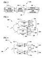
- FIG. 1 shows the eight differential phases used for encoding according to the present invention.
- FIG. 2 is a schematic of a novel optical differential 8-level phase-shift keying transmission system according to the present invention.
- FIG. 3 illustrates a structure of optical demodulators and detectors used in the system shown in FIG. 2 according to a first embodiment of the invention.
- FIG. 4 illustrates another structure of optical demodulators and detectors used in the system shown in FIG. 2 according to a second embodiment of the invention.
- FIG. 5 is a diagram of a first embodiment of optical encoding eight different phases using three cascaded optical modulators.
- FIG. 6 is a schematic diagram of an electrical encoder according to a first embodiment of the invention for use in the system shown in FIG. 2 .
- FIG. 7 is a diagram of a second embodiment of optical encoding using two Mach-Zehnder modulators in a Mach-Zehnder interferometer to cascade a phase modulator.
- FIG. 8 is a diagram of a third embodiment of optical encoding using four Mach-Zehnder modulators in a Mach-Zehnder interferometer.
- optical demodulators 200 MZ interferometer 210 firstarm 212 first demodulator, first arm 214 first detector, first arm 216 second demodulator, first arm 218 second detector, first ann 220 second arm 222 first demodulator, second arm 224 first detector, second arm 226 second demodulator, second arm 228 second detector, second arm 229 XOR gate 300 MZ interferometer 310 first arm 320 second arm.
- first optical demodulator 314 first detector 316 sum/addition 322 second demodulator 324 second detector 326 difference/subtract 400 optical encoder - first embodiment 410 laser source 430 first modulator (I) 440 second modulator (Q) 450 third modulator (D) 500 electrical encoder 600 optical encoder - second embodiment 610 first modulator 620 second modulator 630 third modulator 700 optical encoder - third embodiment 710 first modulator, upper arm 720 second modulator, upper arm 730 first modulator, lower arm 740 second modulator, lower arm
- OD8PSK optical differentiation 8-level phase-shift keying
- eight differential phases between successive bits can have a value of 0, ⁇ /4, ⁇ 2, 3 ⁇ /4, 5 ⁇ /4, 6 ⁇ 4, or 7 ⁇ /4 as shown in FIG. 1 .
- Each encoded symbol carries three bits of information and the symbol rate is one third of the total bit rate.
- FIG. 2 A schematic view of OD8PSK transmission system 100 is shown in FIG. 2 . It comprises an electrical encoder 110 , an optical encoder 120 to produce a differentially encoded optical signal 130 for transmission through an optical transmission medium 140 , and combined optical demodulators and balanced optical detectors 150 .
- the interferometer 200 includes four optical one-bit delayed Mach-Zehnder (MZ) demodulators 212 , 216 , 222 , and 226 and four balanced detectors 214 , 218 , 224 , and 228 for decoding the OD8PSK encoded signals.
- MZ Mach-Zehnder
- the structure of the optical demodulators and detectors is shown in the diagram of FIG. 3 . As shown, the incoming differentially encoded optical signal is divided into two optical signals at a first optical coupler (not shown) for the two arms of the optical demodulator. The two optical signals are further divided to produce separate optical signal for each of the four one-bit delayed optical MZ demodulator.
- an optical 3 dB coupler (not shown) is used for dividing the incoming differentially encoded optical signal into two optical signals for the two arms 210 , 220 .
- Two additional optical 3 dB couplers (not shown), one in each arm 210 , 220 , further divides the two optical signal into four optical signals to be demodulated.
- Each optical demodulator is a one-bit delayed Mach-Zehnder interferometer (MZI) with a phase shift of 3 ⁇ /8, ⁇ /8 and ⁇ /8, and ⁇ 3 ⁇ /8 between two arms 210 , 220 , respectively, of the interferometer 200 .
- a balanced detector is used after each optical demodulator to detect the demodulated signal.
- the demodulators are arranged so that the original input data are recovered directly from the output signals of the receivers. Two input data channels, a and b, are recovered directly at the first arm 210 of the interferometer 200 while the third input data channel, c, is recovered from two balanced receivers, 222 and 224 , through an XOR gate 226 , as shown in the second arm 220 in FIG. 3 .
- each optical demodulator 312 , 322 is a one-bit delayed Mach-Zehnder (MZ) interferometer with a phase shift of ⁇ /8, 3 ⁇ /8 between two arms 310 , 320 of the MZ interferometer 300 .
- a balanced detector 314 , 324 is used after each optical demodulator 312 , 322 to detect the demodulated signal.
- the two original input data, a and b are recovered directly from the output signals of the receivers.
- the third input data channel, c is through electrical processing of the output signals of the receivers.
- the electrical processing includes addition 316 and subtraction 326 of the output signals to generate c 1 and c 2 , respectively.
- the third input data channel, c is recovered from c 1 and c 2 , through an XOR gate 328 , as in FIG. 4 .
- the electrical encoder maps three independent data channels, a, b, and c, into three differentially-encoded data sequences I, Q and D as shown in the schematic diagram of FIG. 6 .
- the encoded data sequences drive optical modulators to generate differentially-encoded optical signal at a symbol rate equal to the bit rate of each input data channel.
- the differentially encoded optical signal is demodulated optically and the original data, a, b and c, are recovered by the receivers (detectors) with direct detection.
- the modulator 420 after the source laser 410 is for return to zero pulse carving. For non-return to zero formats, the modulator 420 is not required.
- the first modulator 430 is a Mach-Zehnder (MZ) modulator biased at transmission null and driven by one (I) of the three encoded outputs of the electrical encoder 500 ( FIG. 6 ) with a peak-to-peak voltage of approximately 2V, so that the encoded phase differences are 0 or ⁇ .
- the second and third modulators 440 and 450 are optical phase modulators with the encoded phase differences of 0 or ⁇ /2 and 0 or ⁇ /4, respectively.
- the electrical encoder maps three independent data channels, a, b, and c, into three differentially-encoded data sequences, I, Q and D, to exactly recover the three original binary input data sequences with the optical encoding and demodulation scheme defined above.
- a schematic diagram of the electrical encoder 500 is shown in FIG. 6 .
- Q [q c + ( q d + q d ) c] ( ab+ ⁇ b )+[ q c+ ( qd+ q d ) c ] ( a b + ⁇ b )
- D ( d c + d c )( ab+ ⁇ b )+( dc+ d c )( a b + ⁇ b )
- I, Q, and D are output of the electrical encoder for a given set of input bits, a, b, and
- another method is used to produce eight different phases with differences that are integer multiple of ⁇ /4 using two MZ modulators 610 , 620 in a MZ interferometer 600 and to cascade a phase modulator as shown in FIG. 7 .
- the two MZ modulators 610 , 620 are biased at transmission null and driven by I and Q, respectively, of three encoded outputs of the electrical encoder 500 ( FIG. 6 ) with a peak-to-peak voltage of approximately 2V.
- the MZ interferometer 600 has differential phase of ⁇ /2 between two arms.
- the encoded output signals from the interferometer has a differential phase between successive bits of 0, ⁇ /2, ⁇ , or 3 ⁇ /2.
- the phase modulator 630 driven by D provides phase changes of 0, ⁇ /4.
- Q d [i ( q ⁇ + q b )+ ⁇ ( q a+q b )]+ d[ ( i ⁇ + ⁇ a ) c+ ( q b + q b ) c ]
- D ( d c + d c )( ab+ ⁇ b )+( dc+ d c )( a b + ⁇ b )
- a third embodiment for optical OD8PSK encoding uses four modulators 710 , 720 , 730 and 740 in a MZ interferometer 700 as shown in FIG. 8 .
- the MZ interferometer 700 also has differential phase 750 of ⁇ /2 between the two arms of the MZ Interferometer 700 .
- the first MZ modulators 710 , 730 in the upper and lower arms are biased at approximately V ⁇ /2 and driven by D and D , respectively, with a voltage of approximately V ⁇ /2 so that the peak power ratio between the outputs from the two modulators is sin ( ⁇ /8)/cos ( ⁇ /8) or cos ( ⁇ /8)/sin ( ⁇ /8).
- the second MZ modulators 720 , 740 in the upper and lower arms are biased at approximately 2V ⁇ transmission null and driven by I and Q, respectively, of three encoded outputs of the electrical encoder with a peak-to-peak voltage of approximately 2V ⁇ .
- the preferred embodiment of the present invention includes an electrical encoder and an optical encoder for generation of differentially encoded 8-level phase-modulated optical signals and optical demodulators and balanced detectors for detection of the optical signals.
- the optical signals are transmitted through optical fiber links or air.
- the electrical encoder maps three independent data channels into three differentially-encoded data sequences.
- the encoded data sequences from the electrical encoder drive optical modulators to generate differentially-encoded 8-level phase modulated optical signals at a symbol rate equal to the bit rate of each input data channel.
- the optical signals After transmission through optical fiber, the optical signals are demodulated optically and the original data are recovered by the balanced detectors with direct detection.
- optical differential 8-level phase-shift keying transmission system of the present invention has been described and illustrated using a particular coding scheme, the description is for illustration only and alternative coding schemes may be substituted. Those skilled in the art will recognize that plural coding methods are available and that the transmission efficiency would be greatly improved when used in conjunction with the optical differential 8-level phase-shift keying transmission system of the present invention.
Abstract
Description
| 100 | |
| 110 | |
| 120 | |
| 130 | differentially encoded |
| 140 | |
| 150 | |
| 200 | |
| 210 | |
| 212 | first demodulator, |
| 214 | first detector, first arm |
| 216 | second demodulator, |
| 218 | second detector, |
| 220 | |
| 222 | first demodulator, |
| 224 | first detector, |
| 226 | second demodulator, |
| 228 | second detector, |
| 229 | |
| 300 | |
| 310 | |
| 320 | second arm. |
| 312 | first |
| 314 | |
| 316 | sum/ |
| 322 | |
| 324 | |
| 326 | difference/ |
| 400 | optical encoder - |
| 410 | |
| 430 | first modulator (I) |
| 440 | second modulator (Q) |
| 450 | third modulator (D) |
| 500 | |
| 600 | optical encoder - |
| 610 | |
| 620 | |
| 630 | |
| 700 | optical encoder - |
| 710 | first modulator, |
| 720 | second modulator, |
| 730 | first modulator, |
| 740 | second modulator, lower arm |
I=
Q=[q
D=(d
where the bar above the symbol indicates a logical inversion, I, Q, and D are output of the electrical encoder for a given set of input bits, a, b, and c, and i, q, and d are the output of the electrical encoder in the previous time slot (i.e. ik=Ik−1, qk=Qk−1, and dk=Dk−1).
I=
Q=
D=(d
I=(iā
Q=(ia
D=[(iq+ī
Claims (16)
I=
Q=[q
D=(d
I=
Q=
D=(d
I=[(
+[(iā
Q=[(ia
+[(
D=[(i
Priority Applications (1)
| Application Number | Priority Date | Filing Date | Title |
|---|---|---|---|
| US11/168,154 US7433604B1 (en) | 2004-07-21 | 2005-06-28 | Direct-detection optical differential 8-level phase shift keying (OD8PSK) for spectrally efficient transmission |
Applications Claiming Priority (2)
| Application Number | Priority Date | Filing Date | Title |
|---|---|---|---|
| US58992204P | 2004-07-21 | 2004-07-21 | |
| US11/168,154 US7433604B1 (en) | 2004-07-21 | 2005-06-28 | Direct-detection optical differential 8-level phase shift keying (OD8PSK) for spectrally efficient transmission |
Publications (1)
| Publication Number | Publication Date |
|---|---|
| US7433604B1 true US7433604B1 (en) | 2008-10-07 |
Family
ID=39797347
Family Applications (1)
| Application Number | Title | Priority Date | Filing Date |
|---|---|---|---|
| US11/168,154 Active 2026-12-06 US7433604B1 (en) | 2004-07-21 | 2005-06-28 | Direct-detection optical differential 8-level phase shift keying (OD8PSK) for spectrally efficient transmission |
Country Status (1)
| Country | Link |
|---|---|
| US (1) | US7433604B1 (en) |
Cited By (10)
| Publication number | Priority date | Publication date | Assignee | Title |
|---|---|---|---|---|
| US20060245764A1 (en) * | 2003-07-01 | 2006-11-02 | Horst Wernz | Transmitter for an optical communication signal |
| US20080056733A1 (en) * | 2006-08-30 | 2008-03-06 | Fujitsu Limited | Phase monitor used in optical receiver |
| US20080166126A1 (en) * | 2004-04-30 | 2008-07-10 | Universitat Stuttgart | Device and Method for Decoding an Optical Multi-Level Dpsk Signal |
| US20080181618A1 (en) * | 2007-01-26 | 2008-07-31 | Cechan Tian | Modulating A Signal According To 2n-PSK Modulation |
| US20100008679A1 (en) * | 2008-07-10 | 2010-01-14 | Finisar Corporation | Phase Shift Keyed Modulation of Optical Signal Using Chirp Managed Laser |
| US20110008054A1 (en) * | 2007-12-14 | 2011-01-13 | Instituto Tecnologico Y De Estudios Superiores De Monterrey | Modulator and demodulator for a differential optical modulation format with eight phase changes |
| US20110200337A1 (en) * | 2010-02-14 | 2011-08-18 | Johnny Karout | Modulation scheme |
| US20120263456A1 (en) * | 2011-04-13 | 2012-10-18 | Fujitsu Limited | Skew suppression method and optical transmission system |
| US8983244B2 (en) | 2011-01-31 | 2015-03-17 | Jds Uniphase Corporation | Optical interferometer |
| US10727937B1 (en) * | 2019-03-01 | 2020-07-28 | Huawei Technologies Co., Ltd. | Multi-layer encoding of optical signals |
Citations (1)
| Publication number | Priority date | Publication date | Assignee | Title |
|---|---|---|---|---|
| US20040081470A1 (en) * | 2000-12-21 | 2004-04-29 | Robert Griffin | Optical communications |
-
2005
- 2005-06-28 US US11/168,154 patent/US7433604B1/en active Active
Patent Citations (1)
| Publication number | Priority date | Publication date | Assignee | Title |
|---|---|---|---|---|
| US20040081470A1 (en) * | 2000-12-21 | 2004-04-29 | Robert Griffin | Optical communications |
Non-Patent Citations (6)
| Title |
|---|
| Han, Y. et al., "Simplified Receiver Implementation for Optical Differential 8-level Phase-Shift Keying", Electronics Letters, vol. 40, No. 21, Oct. 14, 2004. |
| Han, Yan and Guifang Li, "Sensitivity Limits and Degradations in OD8PSK", IEEE Phonetics Technology Letters, Aug. 24, 2004. |
| Kim, C and Li, G., "Direct Detection Differential 8-level Phase Shift Keying (OD8PSK) for Spectrally Efficient Transmission", Optical Society of America (2004). |
| Ohm et al., Differential optical 8-PSK with direct detection (8-DPSK/DD), ITG-Fachtagung, Leipzig, Germany, May 2003, pp. 177-181. * |
| Ohm et al.; Dispersion Compensation and Dispersion Tolerance of Optical 40 Gbit/s DBPSK, DQPSK and 8-DPSK Transmission Systems with RZ and NRZ Impulse Shaping, ITG-Fachtagung, Leipzig, Germany, May 2004. * |
| Ohm; Optical 8-DPSK and receiver with direct detection and multilevel electrical signals; Advanced Modulation Formats, 2004 IEEE/LEOS Workshop on; Jul. 1-2, 2004 pp. 45-46. * |
Cited By (18)
| Publication number | Priority date | Publication date | Assignee | Title |
|---|---|---|---|---|
| US8014683B2 (en) * | 2003-07-01 | 2011-09-06 | Ericsson Ab | Transmitter for an optical communication signal |
| US20060245764A1 (en) * | 2003-07-01 | 2006-11-02 | Horst Wernz | Transmitter for an optical communication signal |
| US20080166126A1 (en) * | 2004-04-30 | 2008-07-10 | Universitat Stuttgart | Device and Method for Decoding an Optical Multi-Level Dpsk Signal |
| US7941058B2 (en) * | 2004-04-30 | 2011-05-10 | Universitat Stuttgart | Device and method for decoding an optical multi-level DPSK signal |
| US20080056733A1 (en) * | 2006-08-30 | 2008-03-06 | Fujitsu Limited | Phase monitor used in optical receiver |
| US7676162B2 (en) * | 2006-08-30 | 2010-03-09 | Fujitsu Limited | Phase monitor used in optical receiver |
| US20080181618A1 (en) * | 2007-01-26 | 2008-07-31 | Cechan Tian | Modulating A Signal According To 2n-PSK Modulation |
| US7860402B2 (en) * | 2007-01-26 | 2010-12-28 | Fujitsu Limited | Modulating a signal according to 2n-PSK modulation |
| US20110008054A1 (en) * | 2007-12-14 | 2011-01-13 | Instituto Tecnologico Y De Estudios Superiores De Monterrey | Modulator and demodulator for a differential optical modulation format with eight phase changes |
| US8687970B2 (en) * | 2007-12-14 | 2014-04-01 | Instituto Tecnologico Y De Estudios Superiores De Monterrey | Modulator and demodulator for a differential optical modulation format with eight phase changes |
| US20100008679A1 (en) * | 2008-07-10 | 2010-01-14 | Finisar Corporation | Phase Shift Keyed Modulation of Optical Signal Using Chirp Managed Laser |
| US8068742B2 (en) * | 2008-07-10 | 2011-11-29 | Finisar Corporation | Phase shift keyed modulation of optical signal using chirp managed laser |
| US20110200337A1 (en) * | 2010-02-14 | 2011-08-18 | Johnny Karout | Modulation scheme |
| US8983244B2 (en) | 2011-01-31 | 2015-03-17 | Jds Uniphase Corporation | Optical interferometer |
| US20120263456A1 (en) * | 2011-04-13 | 2012-10-18 | Fujitsu Limited | Skew suppression method and optical transmission system |
| US8855498B2 (en) * | 2011-04-13 | 2014-10-07 | Fujitsu Limited | Skew suppression method and optical transmission system |
| US10727937B1 (en) * | 2019-03-01 | 2020-07-28 | Huawei Technologies Co., Ltd. | Multi-layer encoding of optical signals |
| JP2022518571A (en) * | 2019-03-01 | 2022-03-15 | 華為技術有限公司 | Multilayer coding of optical signals |
Similar Documents
| Publication | Publication Date | Title |
|---|---|---|
| US7433604B1 (en) | Direct-detection optical differential 8-level phase shift keying (OD8PSK) for spectrally efficient transmission | |
| US7983570B2 (en) | Direct detection differential polarization-phase-shift keying for high spectral efficiency optical communication | |
| US8213806B2 (en) | Optical communications | |
| US7327961B2 (en) | Differential encoder for an optical DQPSK modulator | |
| Sakamoto et al. | 50-Gb/s 16 QAM by a quad-parallel Mach-Zehnder modulator | |
| JP5015288B2 (en) | Optical transmission method and apparatus | |
| CN101895495B (en) | Method and system for transmitting and receiving by orthogonally dual-polarized differential quaternary phase shift keying | |
| US20030198478A1 (en) | Method and system for generating and decoding a bandwidth efficient multi-level signal | |
| JP5182290B2 (en) | Optical modulator and optical communication system | |
| EP2154796B1 (en) | Device and method for receiving a dopsk signal and method for obtaining a dopsk signal | |
| US20090136241A1 (en) | Optical msk data format | |
| US10895797B2 (en) | Line coding for optical transmission | |
| US8873953B2 (en) | Multiple-symbol polarization switching for differential-detection modulation formats | |
| US20110150479A1 (en) | Multi-Level Polarization Multi-Level Phase Modulator | |
| US20100239264A1 (en) | Optical transmission system, apparatus and method | |
| JPH08139681A (en) | Device and system for optical transmission | |
| EP1968215A2 (en) | Apparatus and method for light intensity modulation and optical transmission system employing the same | |
| EP1633061B1 (en) | Method and system for increasing the spectral efficiency of binary coded digital signals | |
| Sakamoto et al. | 50-km SMF transmission of 50-Gb/s 16 QAM generated by quad-parallel MZM | |
| Lu et al. | Mark ratio modulation over pulse position modulation | |
| CN102118337A (en) | Method and device for regenerating phase modulation format signal | |
| Olsson et al. | Electro-optical subcarrier modulation transmitter for 100 GbE DWDM transport | |
| US11677475B2 (en) | Encoding and decoding communications traffic in a pulse amplitude modulation format and optical apparatus for same | |
| TW201145857A (en) | Method for transmitting data on an optical channel | |
| Dong et al. | Generation of 16-Gb/s MSK signal using a single 10-GHz SSB modulator and simplified encoder/decoder |
Legal Events
| Date | Code | Title | Description |
|---|---|---|---|
| AS | Assignment |
Owner name: RESEARCH FOUNDATION OF THE UNIVERSITY OF CENTRAL F Free format text: ASSIGNMENT OF ASSIGNORS INTEREST;ASSIGNORS:KIM, CHEOLHWAN;LI, GUIFANG;HAN, YAN;REEL/FRAME:016744/0960;SIGNING DATES FROM 20050426 TO 20050624 |
|
| STCF | Information on status: patent grant |
Free format text: PATENTED CASE |
|
| FPAY | Fee payment |
Year of fee payment: 4 |
|
| FPAY | Fee payment |
Year of fee payment: 8 |
|
| MAFP | Maintenance fee payment |
Free format text: PAYMENT OF MAINTENANCE FEE, 12TH YR, SMALL ENTITY (ORIGINAL EVENT CODE: M2553); ENTITY STATUS OF PATENT OWNER: SMALL ENTITY Year of fee payment: 12 |