US7428097B1 - Poled structure with inhibition blocks - Google Patents

Poled structure with inhibition blocks Download PDF

Info

Publication number
US7428097B1
US7428097B1 US11/859,648 US85964807A US7428097B1 US 7428097 B1 US7428097 B1 US 7428097B1 US 85964807 A US85964807 A US 85964807A US 7428097 B1 US7428097 B1 US 7428097B1
Authority
US
United States
Prior art keywords
electrode
inhibition
poled structure
combs
strip
Prior art date
Legal status (The legal status is an assumption and is not a legal conclusion. Google has not performed a legal analysis and makes no representation as to the accuracy of the status listed.)
Active
Application number
US11/859,648
Inventor
Tze Chia Lin
Shang Ling Liu
Tso Lun Wu
Ming Hsien Chou
Current Assignee (The listed assignees may be inaccurate. Google has not performed a legal analysis and makes no representation or warranty as to the accuracy of the list.)
HC Photonics Corp
Original Assignee
HC Photonics Corp
Priority date (The priority date is an assumption and is not a legal conclusion. Google has not performed a legal analysis and makes no representation as to the accuracy of the date listed.)
Filing date
Publication date
Application filed by HC Photonics Corp filed Critical HC Photonics Corp
Priority to US11/859,648 priority Critical patent/US7428097B1/en
Assigned to HC PHOTONICS CORP. reassignment HC PHOTONICS CORP. ASSIGNMENT OF ASSIGNORS INTEREST (SEE DOCUMENT FOR DETAILS). Assignors: CHOU, MING HSIEN, LIN, TZE CHIA, LIU, SHANG LING, WU, TSO LUN
Application granted granted Critical
Publication of US7428097B1 publication Critical patent/US7428097B1/en
Active legal-status Critical Current
Anticipated expiration legal-status Critical

Links

Images

Classifications

    • GPHYSICS
    • G02OPTICS
    • G02FOPTICAL DEVICES OR ARRANGEMENTS FOR THE CONTROL OF LIGHT BY MODIFICATION OF THE OPTICAL PROPERTIES OF THE MEDIA OF THE ELEMENTS INVOLVED THEREIN; NON-LINEAR OPTICS; FREQUENCY-CHANGING OF LIGHT; OPTICAL LOGIC ELEMENTS; OPTICAL ANALOGUE/DIGITAL CONVERTERS
    • G02F1/00Devices or arrangements for the control of the intensity, colour, phase, polarisation or direction of light arriving from an independent light source, e.g. switching, gating or modulating; Non-linear optics
    • G02F1/35Non-linear optics
    • G02F1/355Non-linear optics characterised by the materials used
    • G02F1/3558Poled materials, e.g. with periodic poling; Fabrication of domain inverted structures, e.g. for quasi-phase-matching [QPM]
    • GPHYSICS
    • G02OPTICS
    • G02FOPTICAL DEVICES OR ARRANGEMENTS FOR THE CONTROL OF LIGHT BY MODIFICATION OF THE OPTICAL PROPERTIES OF THE MEDIA OF THE ELEMENTS INVOLVED THEREIN; NON-LINEAR OPTICS; FREQUENCY-CHANGING OF LIGHT; OPTICAL LOGIC ELEMENTS; OPTICAL ANALOGUE/DIGITAL CONVERTERS
    • G02F2201/00Constructional arrangements not provided for in groups G02F1/00 - G02F7/00
    • G02F2201/12Constructional arrangements not provided for in groups G02F1/00 - G02F7/00 electrode
    • G02F2201/122Constructional arrangements not provided for in groups G02F1/00 - G02F7/00 electrode having a particular pattern

Definitions

  • the present invention relates to a poled structure, and more particularly, to a poled structure with inhibition blocks to prevent the occurrence of over-poling.
  • the poled structure having poled domains in a ferroelectric single crystal such as lithium niobate (LiNbO 3 ), lithium tantalite (LiTaO 3 ) and potassium titanyl phosphate (KTiOPO 4 ) may be widely used in the optical fields such as optical communication, optical storage and optical measurement.
  • a ferroelectric single crystal such as lithium niobate (LiNbO 3 ), lithium tantalite (LiTaO 3 ) and potassium titanyl phosphate (KTiOPO 4 )
  • There are several methods for preparing the poled structure such as the proton-exchanging method, the electron beam-scanning method, the electric voltage applying method, etc.
  • U.S. Pat. No. 6,002,515 discloses a method for manufacturing a polarization inversion part on a ferroelectric crystal substrate.
  • the polarization inversion part is prepared by steps of applying a voltage in the polarization direction of the ferroelectric crystal substrate to form a polarization inversion part, conducting a heat treatment for reducing an internal electric field generated in the substrate by the applied voltage, and then reinverting polarization in a part of the polarization inversion part by applying a reverse direction voltage against the voltage that was previously applied.
  • the method for preparing a polarization inversion part disclosed in U.S. Pat. No. 6,002,515 requires performing the application of electric voltage twice.
  • U.S. Pat. No. 6,353,495 discloses a method for forming an optical waveguide element.
  • the disclosed method forms a convex ridge portion having a concave portion on a ferroelectric single crystalline substrate, and a ferroelectric single crystalline film is then formed in the concave portion.
  • a comb-shaped electrode and a uniform electrode are formed on a main surface of the ferroelectric single crystalline substrate, and electric voltage is applied to these two electrodes to form a ferroelectric domain-inverted structure in the film in the concave portion.
  • a poled structure comprises a ferroelectric substrate having a top surface and a bottom surface, at least one inhibition block positioned in the ferroelectric substrate, an electrode structure including a first electrode and a second electrode on the top surface and a third electrode in a portion of the bottom surface between the first electrode and the second electrode and a plurality of inverted domains positioned outside of the inhibition block in the ferroelectric substrate.
  • the ferroelectric substrate has a first polarization direction and a first crystal structure
  • the inhibition block has a second crystal structure different from the first crystal structure
  • the inverted domains has a second polarization direction substantially opposite to the first polarization direction.
  • FIG. 1 to FIG. 5 illustrate a method for preparing a poled structure according to the first embodiment of the present invention
  • FIG. 6 and FIG. 7 illustrate a poled structure according to the second embodiment of the present invention
  • FIG. 8 and FIG. 9 illustrate a poled structure according to the third embodiment of the present invention.
  • FIG. 10 and FIG. 11 illustrate a poled structure according to the fourth embodiment of the present invention.
  • FIG. 12 and FIG. 13 illustrate a poled structure according to the fifth embodiment of the present invention.
  • FIG. 14 and FIG. 15 illustrate a poled structure according to the sixth embodiment of the present invention.
  • FIG. 16 and FIG. 17 illustrate a poled structure according to the seventh embodiment of the present invention.
  • FIG. 18 and FIG. 19 illustrate a poled structure according to the eighth embodiment of the present invention.
  • FIG. 1 to FIG. 5 illustrate a method for preparing a poled structure 10 A according to the first embodiment of the present invention, wherein FIG. 2 is a cross-sectional view of FIG. 1 .
  • the method first provides a ferroelectric substrate 12 with a first polarization direction 14 and a first crystal structure, and the ferroelectric substrate 12 has a top surface 12 A and a bottom surface 12 B.
  • a doping process such as a proton-exchanging process or an implanting process, is then performed to form a plurality of inhibition blocks 16 in an upper portion of the ferroelectric substrate 12 , and the inhibition blocks 16 have a second crystal structure different from the first crystal structure, as shown in FIG. 2 .
  • fabrication processes such as metal deposition and etching processes, are then performed to form an electrode structure 20 including a first electrode 22 and a second electrode 24 on the top surface 12 A and a third electrode 26 in a portion of the bottom surface 12 B between the first electrode 22 and the second electrode 24 .
  • the first electrode 22 is a positive electrode including a body 22 A and a plurality of combs 22 B
  • the second electrode 24 is a strip-shaped negative electrode
  • the doping process forms the inhibition blocks 16 between the combs 22 B of the first electrode 22 .
  • the first electrode 22 and the second electrode 24 are separated by a poling area 28 , and the doping process preferably forms the inhibition blocks 16 covering a portion of the poling area 16 near the first electrode 22 .
  • the ferroelectric substrate 12 may include a trench (not shown in the drawings) on the top surface 12 A.
  • a poling process is performed on the electrode structure 20 to form a plurality of inverted domains 30 outside of the inhibition block 16 in the ferroelectric substrate 12 , and the inverted domains 30 have a second polarization direction 32 substantially opposite to the first polarization direction 14 .
  • the poling process is performed by applying a first voltage to the first electrode 22 , a second voltage to the second electrode 24 and a third voltage to the third electrode 26 .
  • the first voltage is higher than the second voltage
  • the first voltage is higher than the third voltage
  • the third voltage is higher than the second voltage or equals to the second voltage.
  • the inhibition blocks 16 near the first electrode 22 can prevent the inverted domains 30 from merging in the ferroelectric substrate 12 between the first electrode 22 and the second electrode 24 such that uniformly deeper periodic inverted domain 30 can be prepared in the ferroelectric substrate 12 .
  • the purpose of the doping process is to change the original crystal structure of the ferroelectric substrate 12 , whose polarization direction cannot be reversed by the subsequent poling process so that the enlarging of the inverted domains 30 due to over-poling can be inhibited.
  • FIG. 6 and FIG. 7 illustrate a poled structure 10 B according to the second embodiment of the present invention.
  • FIG. 6 is a top view of the poled structure 10 B
  • FIG. 7 is a cross-sectional view of the poled structure 10 B.
  • the first electrode 22 of the prepared poled structure 10 B includes a plurality of combs 22 B
  • the second electrode 24 includes a plurality of combs 24 B
  • the doping process forms a plurality of inhibition blocks 16 between the combs 22 B of the first electrode 22 and between the combs 24 B of the second electrode 24 .
  • the first electrode 22 and the second electrode 24 are separated by a poling area 28 , and the doping process forms the inhibition blocks 16 covering a portion of the poling area 28 .
  • the inhibition blocks 16 between the combs 22 B, 24 B of the first electrode 22 and the second electrode 24 can prevent the inverted domain 30 from merging in the ferroelectric substrate 12 between the first electrode 22 and the second electrode 24 such that a uniformly deeper periodic inverted domain 30 can be prepared in the ferroelectric substrate 12 .
  • FIG. 8 and FIG. 9 illustrate a poled structure 10 C according to the third embodiment of the present invention.
  • FIG. 8 is a top view of the poled structure 10 C
  • FIG. 97 is a cross-sectional view of the poled structure 10 C.
  • the first electrode 22 of the prepared poled structure 10 C is a strip-shaped positive electrode
  • the second electrode 24 is a negative electrode including a plurality of combs 24 B
  • the doping process forms the inhibition blocks 16 between the combs 24 B of the second electrode 24 .
  • the first electrode 22 and the second electrode 24 are separated by a poling area 28 , and the doping process forms the inhibition blocks 16 covering a portion of the poling area 28 .
  • the inhibition blocks 16 between the combs 24 B of the second electrode 24 can prevent the inverted domain 30 from merging in the ferroelectric substrate 12 between the first electrode 22 and the second electrode 24 such that a uniformly deeper periodic inverted domain 30 can be prepared in the ferroelectric substrate 12 .
  • FIG. 10 and FIG. 11 illustrate a poled structure 10 D according to the fourth embodiment of the present invention.
  • FIG. 10 is a top view of the poled structure 10 D and
  • FIG. 11 is a cross-sectional view of the poled structure 10 D.
  • the first electrode 22 of the poled structure 10 D is a positive electrode including a plurality of combs 22 B
  • the second electrode 24 is a strip-shaped negative electrode
  • the doping process forms a strip-shaped inhibition block 18 near the second electrode 24 .
  • the first electrode 22 and the second electrode 24 are separated by a poling area 28 , and the doping process forms the strip-shaped inhibition block 18 covering a portion of the poling area 28 near the second electrode 24 .
  • the strip-shaped inhibition block 18 in front of the strip-shaped negative electrode (the second electrode 24 ) can prevent the second electrode 24 from the occurrence of the leakage when the inverted domains 30 reach to the strip-shaped negative electrode 24 from the positive electrode 22 , since the doping process changes the crystal structure of the strip-shaped inhibition block 18 , whose polarization is not easily reversed.
  • FIG. 12 and FIG. 13 illustrate a poled structure 10 E according to the fifth embodiment of the present invention.
  • FIG. 12 is a top view of the poled structure 10 E and
  • FIG. 13 is a cross-sectional view of the poled structure 10 E.
  • the first electrode 22 of the poled structure 10 E is a positive electrode including a plurality of combs 22 B
  • the second electrode 24 is a strip-shaped negative electrode
  • the doping process forms a plurality of inhibition blocks 16 between the combs 22 B and a strip-shaped inhibition block 18 near the second electrode 24 .
  • the first electrode 22 and the second electrode 24 are separated by a poling area 28 , and the doping process forms the inhibition blocks 16 covering a portion of the poling area near the first electrode 22 and the strip-shaped inhibition block 18 covering a portion of the poling area 28 near the second electrode 24 . Due to the application of the inhibition blocks 16 and the strip-shaped inhibition block 18 , this embodiment can not only inhibit over-poling but also prevent leakage, and the inverted domains 30 can be prepared more uniformly.
  • FIG. 14 and FIG. 15 illustrate a poled structure 10 F according to the sixth embodiment of the present invention.
  • FIG. 14 is a top view of the poled structure 10 F
  • FIG. 15 is a cross-sectional view of the poled structure 10 F.
  • the first electrode 22 of the poled structure 10 F includes a plurality of combs 22 B
  • the second electrode 24 includes a plurality of combs 24 B
  • the doping process forms a plurality of inhibition blocks 16 between the combs 22 B of the first electrode 22 and a strip-shaped inhibition block 18 near the second electrode 24 .
  • the first electrode 22 and the second electrode 24 are separated by a poling area 28 , and the doping process forms the inhibition blocks 16 covering a portion of the poling area 28 near the first electrode 22 and the strip-shaped inhibition block 18 covering a portion of the poling area 28 near the second electrode 24 . Due to the application of the inhibition blocks 16 and the strip-shaped inhibition block 18 , this embodiment can not only inhibit over-poling but also prevent leakage, and the inverted domains 30 can be prepared more uniformly.
  • FIG. 16 and FIG. 17 illustrate a poled structure 10 G according to the seventh embodiment of the present invention.
  • FIG. 16 is a top view of the poled structure 10 G
  • FIG. 17 is a cross-sectional view of the poled structure 10 G.
  • the first electrode 22 of the poled structure 10 G includes a plurality of combs 22 B, the doping process forms a strip-shaped inhibition block 18 in the ferroelectric substrate 12 , and the second electrode 24 is formed on the strip-shaped inhibition block 18 .
  • the strip-shaped inhibition block 18 under the strip-shaped negative electrode 24 supports the conductivity and serves as the extension of the strip-shaped negative electrode 24 , which can increase the internal electrical field as the poling process is performed by applying voltages to the positive electrode 22 and the negative electrode 24 , and the increased internal electrical field is contributory to the formation of the inverted domains 30 .
  • FIG. 18 and FIG. 19 illustrate a poled structure 10 H according to the eighth embodiment of the present invention.
  • FIG. 18 is a top view of the poled structure 10 H
  • FIG. 19 is a cross-sectional view of the poled structure 10 H.
  • the first electrode 22 of the poled structure 10 H includes a plurality of combs 22 B
  • the doping process forms a plurality of inhibition blocks 16 in the ferroelectric substrate 12
  • the second electrode 24 is formed on the inhibition blocks 16 .
  • the inhibition block 16 under the strip-shaped negative electrode 24 supports the conductivity and serves as the extension of the strip-shaped negative electrode 24 , which can increase the internal electrical field as the poling process is performed by applying voltages to the positive electrode 22 and the negative electrode 24 , and the increased internal electrical field is contributory to the formation of the inverted domains 30 .
  • FIG. 20 and FIG. 21 illustrate a poled structure 10 I according to the ninth embodiment of the present invention.
  • FIG. 20 is a top view of the poled structure 10 I
  • FIG. 21 is a cross-sectional view of the poled structure 10 I.
  • the first electrode 22 of the poled structure 10 I includes a plurality of combs 22 B
  • the doping process forms a plurality of inhibition blocks 16 between the combs 22 B and a strip-shaped inhibition block 18 in the ferroelectric substrate 12
  • the second electrode 24 is formed on the strip-shaped inhibition block 18 .
  • the strip-shaped inhibition blocks 16 between the combs 24 B of the positive electrode 22 can inhibit over-poling and the strip-shaped inhibition block 18 under the negative electrode 24 can increase the internal field to help the formulation of inverted domains 30 uniformly.

Landscapes

  • Physics & Mathematics (AREA)
  • Nonlinear Science (AREA)
  • General Physics & Mathematics (AREA)
  • Optics & Photonics (AREA)
  • Optical Modulation, Optical Deflection, Nonlinear Optics, Optical Demodulation, Optical Logic Elements (AREA)

Abstract

A poled structure comprises a ferroelectric substrate having a top surface and a bottom surface, at least one inhibition block positioned in the ferroelectric substrate, an electrode structure including a first electrode and a second electrode on the top surface and a third electrode in a portion of the bottom surface between the first electrode and the second electrode and a plurality of inverted domains positioned outside of the inhibition block in the ferroelectric substrate. The ferroelectric substrate has a first polarization direction and a first crystal structure, the inhibition block has a second crystal structure different from the first crystal structure, and the inverted domains has a second polarization direction substantially opposite to the first polarization direction.

Description

BACKGROUND OF THE INVENTION
(A) Field of the Invention
The present invention relates to a poled structure, and more particularly, to a poled structure with inhibition blocks to prevent the occurrence of over-poling.
(B) Description of the Related Art
The poled structure having poled domains in a ferroelectric single crystal such as lithium niobate (LiNbO3), lithium tantalite (LiTaO3) and potassium titanyl phosphate (KTiOPO4) may be widely used in the optical fields such as optical communication, optical storage and optical measurement. There are several methods for preparing the poled structure such as the proton-exchanging method, the electron beam-scanning method, the electric voltage applying method, etc.
U.S. Pat. No. 6,002,515 discloses a method for manufacturing a polarization inversion part on a ferroelectric crystal substrate. The polarization inversion part is prepared by steps of applying a voltage in the polarization direction of the ferroelectric crystal substrate to form a polarization inversion part, conducting a heat treatment for reducing an internal electric field generated in the substrate by the applied voltage, and then reinverting polarization in a part of the polarization inversion part by applying a reverse direction voltage against the voltage that was previously applied. In other words, the method for preparing a polarization inversion part disclosed in U.S. Pat. No. 6,002,515 requires performing the application of electric voltage twice.
U.S. Pat. No. 6,353,495 discloses a method for forming an optical waveguide element. The disclosed method forms a convex ridge portion having a concave portion on a ferroelectric single crystalline substrate, and a ferroelectric single crystalline film is then formed in the concave portion. A comb-shaped electrode and a uniform electrode are formed on a main surface of the ferroelectric single crystalline substrate, and electric voltage is applied to these two electrodes to form a ferroelectric domain-inverted structure in the film in the concave portion.
SUMMARY OF THE INVENTION
One aspect of the present invention provides a poled structure with inhibition blocks to prevent the occurrence of over-poling.
A poled structure according to this aspect of the present invention comprises a ferroelectric substrate having a top surface and a bottom surface, at least one inhibition block positioned in the ferroelectric substrate, an electrode structure including a first electrode and a second electrode on the top surface and a third electrode in a portion of the bottom surface between the first electrode and the second electrode and a plurality of inverted domains positioned outside of the inhibition block in the ferroelectric substrate. The ferroelectric substrate has a first polarization direction and a first crystal structure, the inhibition block has a second crystal structure different from the first crystal structure, and the inverted domains has a second polarization direction substantially opposite to the first polarization direction.
BRIEF DESCRIPTION OF THE DRAWINGS
The objectives and advantages of the present invention will become apparent upon reading the following description and upon reference to the accompanying drawings in which:
FIG. 1 to FIG. 5 illustrate a method for preparing a poled structure according to the first embodiment of the present invention;
FIG. 6 and FIG. 7 illustrate a poled structure according to the second embodiment of the present invention;
FIG. 8 and FIG. 9 illustrate a poled structure according to the third embodiment of the present invention;
FIG. 10 and FIG. 11 illustrate a poled structure according to the fourth embodiment of the present invention;
FIG. 12 and FIG. 13 illustrate a poled structure according to the fifth embodiment of the present invention;
FIG. 14 and FIG. 15 illustrate a poled structure according to the sixth embodiment of the present invention;
FIG. 16 and FIG. 17 illustrate a poled structure according to the seventh embodiment of the present invention; and
FIG. 18 and FIG. 19 illustrate a poled structure according to the eighth embodiment of the present invention.
DETAILED DESCRIPTION OF THE INVENTION
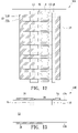
FIG. 1 to FIG. 5 illustrate a method for preparing a poled structure 10A according to the first embodiment of the present invention, wherein FIG. 2 is a cross-sectional view of FIG. 1. The method first provides a ferroelectric substrate 12 with a first polarization direction 14 and a first crystal structure, and the ferroelectric substrate 12 has a top surface 12A and a bottom surface 12B. Subsequently, a doping process, such as a proton-exchanging process or an implanting process, is then performed to form a plurality of inhibition blocks 16 in an upper portion of the ferroelectric substrate 12, and the inhibition blocks 16 have a second crystal structure different from the first crystal structure, as shown in FIG. 2.
Referring to FIG. 3 and FIG. 4, fabrication processes, such as metal deposition and etching processes, are then performed to form an electrode structure 20 including a first electrode 22 and a second electrode 24 on the top surface 12A and a third electrode 26 in a portion of the bottom surface 12B between the first electrode 22 and the second electrode 24. In particular, the first electrode 22 is a positive electrode including a body 22A and a plurality of combs 22B, the second electrode 24 is a strip-shaped negative electrode, and the doping process forms the inhibition blocks 16 between the combs 22B of the first electrode 22. Furthermore, the first electrode 22 and the second electrode 24 are separated by a poling area 28, and the doping process preferably forms the inhibition blocks 16 covering a portion of the poling area 16 near the first electrode 22. Optionally, the ferroelectric substrate 12 may include a trench (not shown in the drawings) on the top surface 12A.
Referring to FIG. 5, a poling process is performed on the electrode structure 20 to form a plurality of inverted domains 30 outside of the inhibition block 16 in the ferroelectric substrate 12, and the inverted domains 30 have a second polarization direction 32 substantially opposite to the first polarization direction 14. Preferably, the poling process is performed by applying a first voltage to the first electrode 22, a second voltage to the second electrode 24 and a third voltage to the third electrode 26. Preferably, the first voltage is higher than the second voltage, the first voltage is higher than the third voltage, and the third voltage is higher than the second voltage or equals to the second voltage.
In particular, the inhibition blocks 16 near the first electrode 22 can prevent the inverted domains 30 from merging in the ferroelectric substrate 12 between the first electrode 22 and the second electrode 24 such that uniformly deeper periodic inverted domain 30 can be prepared in the ferroelectric substrate 12. The purpose of the doping process is to change the original crystal structure of the ferroelectric substrate 12, whose polarization direction cannot be reversed by the subsequent poling process so that the enlarging of the inverted domains 30 due to over-poling can be inhibited.
FIG. 6 and FIG. 7 illustrate a poled structure 10B according to the second embodiment of the present invention. FIG. 6 is a top view of the poled structure 10B and FIG. 7 is a cross-sectional view of the poled structure 10B. Compared with the prepared poled structure 10A in FIG. 5, the first electrode 22 of the prepared poled structure 10B includes a plurality of combs 22B, the second electrode 24 includes a plurality of combs 24B, and the doping process forms a plurality of inhibition blocks 16 between the combs 22B of the first electrode 22 and between the combs 24B of the second electrode 24. In particular, the first electrode 22 and the second electrode 24 are separated by a poling area 28, and the doping process forms the inhibition blocks 16 covering a portion of the poling area 28. The inhibition blocks 16 between the combs 22B, 24B of the first electrode 22 and the second electrode 24 can prevent the inverted domain 30 from merging in the ferroelectric substrate 12 between the first electrode 22 and the second electrode 24 such that a uniformly deeper periodic inverted domain 30 can be prepared in the ferroelectric substrate 12.
FIG. 8 and FIG. 9 illustrate a poled structure 10C according to the third embodiment of the present invention. FIG. 8 is a top view of the poled structure 10C and FIG. 97 is a cross-sectional view of the poled structure 10C. Compared with the prepared poled structure 10A in FIG. 5, the first electrode 22 of the prepared poled structure 10C is a strip-shaped positive electrode, the second electrode 24 is a negative electrode including a plurality of combs 24B, and the doping process forms the inhibition blocks 16 between the combs 24B of the second electrode 24. In particular, the first electrode 22 and the second electrode 24 are separated by a poling area 28, and the doping process forms the inhibition blocks 16 covering a portion of the poling area 28. The inhibition blocks 16 between the combs 24B of the second electrode 24 can prevent the inverted domain 30 from merging in the ferroelectric substrate 12 between the first electrode 22 and the second electrode 24 such that a uniformly deeper periodic inverted domain 30 can be prepared in the ferroelectric substrate 12.
FIG. 10 and FIG. 11 illustrate a poled structure 10D according to the fourth embodiment of the present invention. FIG. 10 is a top view of the poled structure 10D and FIG. 11 is a cross-sectional view of the poled structure 10D. Compared with the prepared poled structure 10A in FIG. 5, the first electrode 22 of the poled structure 10D is a positive electrode including a plurality of combs 22B, the second electrode 24 is a strip-shaped negative electrode, and the doping process forms a strip-shaped inhibition block 18 near the second electrode 24. Preferably, the first electrode 22 and the second electrode 24 are separated by a poling area 28, and the doping process forms the strip-shaped inhibition block 18 covering a portion of the poling area 28 near the second electrode 24. The strip-shaped inhibition block 18 in front of the strip-shaped negative electrode (the second electrode 24) can prevent the second electrode 24 from the occurrence of the leakage when the inverted domains 30 reach to the strip-shaped negative electrode 24 from the positive electrode 22, since the doping process changes the crystal structure of the strip-shaped inhibition block 18, whose polarization is not easily reversed.
FIG. 12 and FIG. 13 illustrate a poled structure 10E according to the fifth embodiment of the present invention. FIG. 12 is a top view of the poled structure 10E and FIG. 13 is a cross-sectional view of the poled structure 10E. Compared with the prepared poled structure 10A in FIG. 5, the first electrode 22 of the poled structure 10E is a positive electrode including a plurality of combs 22B, the second electrode 24 is a strip-shaped negative electrode, and the doping process forms a plurality of inhibition blocks 16 between the combs 22B and a strip-shaped inhibition block 18 near the second electrode 24. Preferably, the first electrode 22 and the second electrode 24 are separated by a poling area 28, and the doping process forms the inhibition blocks 16 covering a portion of the poling area near the first electrode 22 and the strip-shaped inhibition block 18 covering a portion of the poling area 28 near the second electrode 24. Due to the application of the inhibition blocks 16 and the strip-shaped inhibition block 18, this embodiment can not only inhibit over-poling but also prevent leakage, and the inverted domains 30 can be prepared more uniformly.
FIG. 14 and FIG. 15 illustrate a poled structure 10F according to the sixth embodiment of the present invention. FIG. 14 is a top view of the poled structure 10F and FIG. 15 is a cross-sectional view of the poled structure 10F. Compared with the prepared poled structure 10A in FIG. 5, the first electrode 22 of the poled structure 10F includes a plurality of combs 22B, the second electrode 24 includes a plurality of combs 24B, and the doping process forms a plurality of inhibition blocks 16 between the combs 22B of the first electrode 22 and a strip-shaped inhibition block 18 near the second electrode 24. Preferably, the first electrode 22 and the second electrode 24 are separated by a poling area 28, and the doping process forms the inhibition blocks 16 covering a portion of the poling area 28 near the first electrode 22 and the strip-shaped inhibition block 18 covering a portion of the poling area 28 near the second electrode 24. Due to the application of the inhibition blocks 16 and the strip-shaped inhibition block 18, this embodiment can not only inhibit over-poling but also prevent leakage, and the inverted domains 30 can be prepared more uniformly.
FIG. 16 and FIG. 17 illustrate a poled structure 10G according to the seventh embodiment of the present invention. FIG. 16 is a top view of the poled structure 10G and FIG. 17 is a cross-sectional view of the poled structure 10G. Compared with the prepared poled structure 10A in FIG. 5, the first electrode 22 of the poled structure 10G includes a plurality of combs 22B, the doping process forms a strip-shaped inhibition block 18 in the ferroelectric substrate 12, and the second electrode 24 is formed on the strip-shaped inhibition block 18. In particular, the strip-shaped inhibition block 18 under the strip-shaped negative electrode 24 supports the conductivity and serves as the extension of the strip-shaped negative electrode 24, which can increase the internal electrical field as the poling process is performed by applying voltages to the positive electrode 22 and the negative electrode 24, and the increased internal electrical field is contributory to the formation of the inverted domains 30.
FIG. 18 and FIG. 19 illustrate a poled structure 10H according to the eighth embodiment of the present invention. FIG. 18 is a top view of the poled structure 10H and FIG. 19 is a cross-sectional view of the poled structure 10H. Compared with the prepared poled structure 10A in FIG. 5, the first electrode 22 of the poled structure 10H includes a plurality of combs 22B, the doping process forms a plurality of inhibition blocks 16 in the ferroelectric substrate 12, and the second electrode 24 is formed on the inhibition blocks 16. In particular, the inhibition block 16 under the strip-shaped negative electrode 24 supports the conductivity and serves as the extension of the strip-shaped negative electrode 24, which can increase the internal electrical field as the poling process is performed by applying voltages to the positive electrode 22 and the negative electrode 24, and the increased internal electrical field is contributory to the formation of the inverted domains 30.
FIG. 20 and FIG. 21 illustrate a poled structure 10I according to the ninth embodiment of the present invention. FIG. 20 is a top view of the poled structure 10I and FIG. 21 is a cross-sectional view of the poled structure 10I. Compared with the prepared poled structure 10A in FIG. 5, the first electrode 22 of the poled structure 10I includes a plurality of combs 22B, the doping process forms a plurality of inhibition blocks 16 between the combs 22B and a strip-shaped inhibition block 18 in the ferroelectric substrate 12, and the second electrode 24 is formed on the strip-shaped inhibition block 18. In particular, the strip-shaped inhibition blocks 16 between the combs 24B of the positive electrode 22 can inhibit over-poling and the strip-shaped inhibition block 18 under the negative electrode 24 can increase the internal field to help the formulation of inverted domains 30 uniformly.
The above-described embodiments of the present invention are intended to be illustrative only. Numerous alternative embodiments may be devised by those skilled in the art without departing from the scope of the following claims.

Claims (19)

1. A poled structure, comprising:
a ferroelectric substrate with a first polarization direction and a first crystal structure, and the ferroelectric substrate having a top surface and a bottom surface;
at least one inhibition block positioned in the ferroelectric substrate, and the inhibition block having a second crystal structure different from the first crystal structure; and
an electrode structure including a first electrode and a second electrode on the top surface and a third electrode in a portion of the bottom surface between the first electrode and the second electrode.
2. The poled structure as claimed in claim 1, wherein the inhibition block is formed in an upper portion of the ferroelectric substrate.
3. The poled structure as claimed in claim 1, wherein the first electrode is a positive electrode including a plurality of combs, the second electrode is a strip-shaped negative electrode, and the doping process forms a plurality of inhibition blocks between the combs of the first electrode.
4. The poled structure as claimed in claim 3, wherein the first electrode and the second electrode are separated by a poling area, and the inhibition blocks cover a portion of the poling area near the first electrode.
5. The poled structure as claimed in claim 1, wherein the first electrode includes a plurality of combs, the second electrode includes a plurality of combs, and a plurality of inhibition blocks are positioned between the combs.
6. The poled structure as claimed in claim 5, wherein the first electrode and the second electrode are separated by a poling area, and the inhibition blocks cover a portion of the poling area.
7. The poled structure as claimed in claim 1, wherein the first electrode is a strip-shaped positive electrode, the second electrode is a negative electrode including a plurality of combs, and a plurality of inhibition blocks are positioned between the combs of the second electrode.
8. The poled structure as claimed in claim 7, wherein the first electrode and the second electrode are separated by a poling area, and the inhibition blocks cover a portion of the poling area.
9. The poled structure as claimed in claim 1, wherein the first electrode is a positive electrode including a plurality of combs, the second electrode is a strip-shaped negative electrode, and an inhibition block is positioned near the second electrode.
10. The poled structure as claimed in claim 9, wherein the first electrode and the second electrode are separated by a poling area, and the inhibition block is a strip-shaped inhibition block covers a portion of the poling area near the second electrode.
11. The poled structure as claimed in claim 1, wherein the first electrode is a positive electrode including a plurality of combs, the second electrode is a strip-shaped negative electrode, and a plurality of first inhibition blocks are positioned between the combs and a second inhibition block near the second electrode.
12. The poled structure as claimed in claim 11, wherein the first electrode and the second electrode are separated by a poling area, and the first inhibition blocks covers a portion of the poling area near the first electrode and the second inhibition block covers a portion of the poling area near the second electrode.
13. The poled structure as claimed in claim 1, wherein the first electrode includes a plurality of combs, the second electrode includes a plurality of combs, and a plurality of first inhibition blocks are positioned between the combs of the first electrode and a second inhibition block is positioned near the second electrode.
14. The poled structure as claimed in claim 13, wherein the first electrode and the second electrode are separated by a poling area, and the first inhibition blocks covers a portion of the poling area near the first electrode and the second inhibition block covers a portion of the poling area near the second electrode.
15. The poled structure as claimed in claim 1, wherein the first electrode includes a plurality of combs, a strip-shaped inhibition block is positioned in the ferroelectric substrate, and the second electrode is formed on the strip-shaped inhibition block.
16. The poled structure as claimed in claim 1, wherein the first electrode includes a plurality of combs, a plurality of inhibition blocks are positioned in the ferroelectric substrate, and the second electrode is formed on the inhibition blocks.
17. The poled structure as claimed in claim 1, wherein the first electrode includes a plurality of combs, a plurality of first inhibition blocks are positioned between the combs and a second inhibition block is positioned in the ferroelectric substrate, and the second electrode is formed on the second inhibition block.
18. The poled structure as claimed in claim 1, wherein the ferroelectric substrate includes a trench on the top surface.
19. The poled structure as claimed in claim 1, further comprising a plurality of inverted domains positioned outside of the inhibition block in the ferroelectric substrate, and the inverted domains having a second polarization direction substantially opposite to the first polarization direction.
US11/859,648 2007-09-21 2007-09-21 Poled structure with inhibition blocks Active US7428097B1 (en)

Priority Applications (1)

Application Number Priority Date Filing Date Title
US11/859,648 US7428097B1 (en) 2007-09-21 2007-09-21 Poled structure with inhibition blocks

Applications Claiming Priority (1)

Application Number Priority Date Filing Date Title
US11/859,648 US7428097B1 (en) 2007-09-21 2007-09-21 Poled structure with inhibition blocks

Publications (1)

Publication Number Publication Date
US7428097B1 true US7428097B1 (en) 2008-09-23

Family

ID=39764185

Family Applications (1)

Application Number Title Priority Date Filing Date
US11/859,648 Active US7428097B1 (en) 2007-09-21 2007-09-21 Poled structure with inhibition blocks

Country Status (1)

Country Link
US (1) US7428097B1 (en)

Citations (3)

* Cited by examiner, † Cited by third party
Publication number Priority date Publication date Assignee Title
US6002515A (en) 1997-01-14 1999-12-14 Matsushita Electric Industrial Co., Ltd. Method for producing polarization inversion part, optical wavelength conversion element using the same, and optical waveguide
US6353495B1 (en) 1998-08-18 2002-03-05 Matsushita Electric Industrial Co., Ltd. Method for forming a ferroelectric domain-inverted structure
US20070258131A1 (en) * 2004-10-14 2007-11-08 Ngk Insulators, Ltd. Method for fabricating polarization reversal structure and reversal structure

Patent Citations (3)

* Cited by examiner, † Cited by third party
Publication number Priority date Publication date Assignee Title
US6002515A (en) 1997-01-14 1999-12-14 Matsushita Electric Industrial Co., Ltd. Method for producing polarization inversion part, optical wavelength conversion element using the same, and optical waveguide
US6353495B1 (en) 1998-08-18 2002-03-05 Matsushita Electric Industrial Co., Ltd. Method for forming a ferroelectric domain-inverted structure
US20070258131A1 (en) * 2004-10-14 2007-11-08 Ngk Insulators, Ltd. Method for fabricating polarization reversal structure and reversal structure

Similar Documents

Publication Publication Date Title
EP0532969B1 (en) Process for fabricating an optical device for generating a second harmonic optical beam
CN1147860A (en) Fabrication of Patterned Polarized Dielectric Material Structures and Devices
CN103901698A (en) Electrode structure manufacturing method for suppressing reversal domain lateral growth in ferroelectric crystal material polarization process
US7486432B2 (en) Method for preparing a periodically poled structure
JPH04104233A (en) Optical waveguide device and production thereof
US12007666B2 (en) Wavelength conversion element and method for producing same
US7428097B1 (en) Poled structure with inhibition blocks
JP3999362B2 (en) Method for producing ferroelectric crystal having periodic domain-inverted structure
US7474458B1 (en) Method for preparing a poled structure with inhibition blocks
Nagy et al. Periodic poling of ion-sliced X-cut magnesium oxide doped lithium niobate thin films
US20090080062A1 (en) Method for preparing a poled structure by using double-sided electrodes
US7515794B1 (en) Periodically poled element having a suppressing structure for the domain spreading
Horikawa et al. Formation of domain-inverted grating in MgO: LiNbO3 by voltage application with insulation layer cladding
Lee et al. Periodical domain inversion in singlemode Ti: MgO: LiNbO3 channel waveguides
US20080160175A1 (en) Method for Preparing a Periodically Poled Structure
US7502163B1 (en) Method for preparing a poled structure by using leakage and tunnel effects
US7394588B2 (en) Wavelength converter structure and method for preparing the same
US7446930B2 (en) Method of inverting polarization by controlling defect density or degree of order of lattice points
JP2004070207A (en) Method of manufacturing polarization reversal crystal
JP6019618B2 (en) Method for forming periodic domain-inverted structure and method for forming wavelength conversion element
JP2003307757A (en) Method for manufacturing domain inversion part
JP4514146B2 (en) Method for manufacturing periodically poled optical waveguide device
Janner et al. Grinding free electric-field poling of Ti indiffused z-cut LiNbO3 wafer with submicron resolution
RU2439636C1 (en) Method of forming domain structure in monocrystalline wafer of nonlinear-optic ferroelectric material
GB2368402A (en) Stabilising polar and ferroelectric devices

Legal Events

Date Code Title Description
AS Assignment

Owner name: HC PHOTONICS CORP., TAIWAN

Free format text: ASSIGNMENT OF ASSIGNORS INTEREST;ASSIGNORS:LIN, TZE CHIA;LIU, SHANG LING;WU, TSO LUN;AND OTHERS;REEL/FRAME:019862/0582

Effective date: 20070427

STCF Information on status: patent grant

Free format text: PATENTED CASE

FPAY Fee payment

Year of fee payment: 4

FPAY Fee payment

Year of fee payment: 8

MAFP Maintenance fee payment

Free format text: PAYMENT OF MAINTENANCE FEE, 12TH YR, SMALL ENTITY (ORIGINAL EVENT CODE: M2553); ENTITY STATUS OF PATENT OWNER: SMALL ENTITY

Year of fee payment: 12