US7395039B2 - Transmitter - Google Patents
Transmitter Download PDFInfo
- Publication number
- US7395039B2 US7395039B2 US11/282,597 US28259705A US7395039B2 US 7395039 B2 US7395039 B2 US 7395039B2 US 28259705 A US28259705 A US 28259705A US 7395039 B2 US7395039 B2 US 7395039B2
- Authority
- US
- United States
- Prior art keywords
- radio
- amplitude component
- voltage
- amplitude
- modulated signal
- Prior art date
- Legal status (The legal status is an assumption and is not a legal conclusion. Google has not performed a legal analysis and makes no representation as to the accuracy of the status listed.)
- Expired - Fee Related, expires
Links
Images


Classifications
-
- H—ELECTRICITY
- H03—ELECTRONIC CIRCUITRY
- H03G—CONTROL OF AMPLIFICATION
- H03G3/00—Gain control in amplifiers or frequency changers
- H03G3/20—Automatic control
- H03G3/30—Automatic control in amplifiers having semiconductor devices
- H03G3/3036—Automatic control in amplifiers having semiconductor devices in high-frequency amplifiers or in frequency-changers
- H03G3/3042—Automatic control in amplifiers having semiconductor devices in high-frequency amplifiers or in frequency-changers in modulators, frequency-changers, transmitters or power amplifiers
-
- H—ELECTRICITY
- H03—ELECTRONIC CIRCUITRY
- H03C—MODULATION
- H03C5/00—Amplitude modulation and angle modulation produced simultaneously or at will by the same modulating signal
-
- H—ELECTRICITY
- H04—ELECTRIC COMMUNICATION TECHNIQUE
- H04L—TRANSMISSION OF DIGITAL INFORMATION, e.g. TELEGRAPHIC COMMUNICATION
- H04L27/00—Modulated-carrier systems
- H04L27/26—Systems using multi-frequency codes
- H04L27/2601—Multicarrier modulation systems
- H04L27/2626—Arrangements specific to the transmitter only
Definitions
- the present invention relates to a radio transmitter used for communication methods using subcarriers such as the OFDM (orthogonal frequency division multiplex).
- subcarriers such as the OFDM (orthogonal frequency division multiplex).
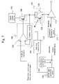
- FIG. 8 is a block diagram showing the EER method in outline.
- a modulated signal for example a QAM signal
- outputted from an OFDM signal generation circuit 100 as modulated signal generating means is divided into two branches.
- the modulated signal is upconverted by a quadrature modulation circuit 111 , and inputted as a radio-frequency modulated wave to a radio-frequency modulated signal input terminal of a radio-frequency power amplifier 112 comprising a saturated amplifier.
- the modulated signal is converted to an amplitude component by an amplitude extraction circuit 101 , amplified to a desired amplitude component voltage level by an operational amplifier 103 , and inputted to an emitter follower 106 as voltage converting means.
- reference numeral 102 represents an amplitude amplification circuit as amplitude amplifying means
- reference numeral 104 represent a feedback circuit
- reference numeral 105 represents a supply voltage portion.
- the radio-frequency power amplifier 112 When a radio-frequency modulated wave which is an input signal is amplified by the radio-frequency power amplifier 112 comprising a saturated amplifier, the amplitude component of the radio-frequency modulated wave is temporarily lost in the process. However, when the supply voltage of the radio-frequency power amplifier 112 is controlled in proportion to the amplitude component of the radio-frequency modulated wave which is the input signal, the amplitude component of the radio-frequency modulated wave is inputted from the supply voltage portion 105 to the supply voltage terminal of the radio-frequency power amplifier 112 . As a result, a radio-frequency modulated wave containing the original amplitude component which radio-frequency modulated wave is restored at the radio-frequency power amplifier 112 is outputted.
- this structure enables the radio-frequency power amplifier to operate in a highly efficient saturated condition even when the amplitude component of the modulated signal is changed, so that the efficiency of the radio-frequency power amplifier 112 can be enhanced.
- the saturated amplifier refers to a Class-F amplifier where harmonic control is performed so that the drain voltage waveform is rectangular, or a Class-E or a Class-D amplifier where the load condition is optimized so that the drain voltage waveform and the drain current waveform do not overlap each other.
- the saturated amplifier since the period during which the drain current and the drain voltage are simultaneously generated is minimized as a characteristic thereof, power consumption can be suppressed.
- the DC power is 600 mW.
- the saturated amplifier as the radio-frequency power amplifier 112 , no current flows when the field-effect transistor is off, and only the supply voltage is applied. Consequently, the DC power consumption is 0.
- the drain-source voltage VDS is a saturated voltage, that is, 0.3 V at the most.
- the original modulated signal (precisely, radio-frequency modulated wave since the original modulated signal is frequency-converted) cannot be reproduced. That is, the errors of the amplitude component and the phase component appear as a spectral distortion of the outputted radio-frequency modulated wave and degradation in modulation accuracy.
- the transmission path of the amplitude component it is necessary for the transmission path of the amplitude component to have a closed loop structure having a feedback circuit so that the error component reaching the supply voltage terminal of the radio-frequency power amplifier is reduced.
- the saturated amplifier When the saturated amplifier is used in a completely saturated region, the amount of fluctuations in the phase change with respect to the change in the amplitude component inputted to the supply voltage terminal of the radio-frequency power amplifier is increased, so that the arithmetic throughput of the inverse correction processing is increased.
- the characteristic of the radio-frequency power amplifier is changed due to fluctuations in temperature or power, since the amount of fluctuations in the error function is increased, a spectral distortion or degradation in modulation accuracy occurs in the radio-frequency modulated wave as a result.
- the saturated amplifier characteristic to be used a region that is not completely saturated, that is, a region close to the saturated region, for example, the 1-dB gain compression point is used.
- Patent Document 1 U.S. Pat. No. 5,251,330A1
- the modulated signal in a modulated signal with a high PAPR and high instantaneous peak power like that of the IEEE 802.11a/g standard which is a wireless LAN standard, there are cases where by the transmitter characteristic fluctuating, a time delay occurs between a first amplitude component outputted from the amplitude extraction circuit 101 and a second amplitude component of a radio-frequency modulated wave inputted to the radio-frequency modulated signal input terminal of the radio-frequency power amplifier 112 , amplified and occurring at the output terminal of the radio-frequency power amplifier 112 .
- the following problem arises:
- the second amplitude component leaks to the feedback circuit 104 as shown in FIG. 8
- the leakage component and the first amplitude component are superimposed on each other in the feedback circuit 104 .
- This causes ringing due to a transient response, so that the amplitude component outputted from the amplitude amplification circuit 102 constituting the closed loop oscillates without converging. Consequently, the modulated waveform cannot be reproduced and a distortion occurs at the output terminal of the radio-frequency power amplifier 112 , that is, the saturated amplifier.
- the modulated signal in a modulated wave where the PAPR is high and the difference between the average power and the instantaneous peak power is large like that of the IEEE 802.11a/g standard which is a wireless LAN standard, in a linear amplifier where no amplitude component is required of the supply voltage of the radio-frequency power amplifier, a large capacitance can be set in the vicinity of the supply voltage terminal in order to suppress the modulated wave characteristic degradation due to supply voltage fluctuations.
- the supply voltage terminal of the radio-frequency power amplifier it is necessary for the supply voltage terminal of the radio-frequency power amplifier to linearly transmit an amplitude component having a frequency component of, for example, approximately 40 MHz. For this reason, a capacitance having a high capacitance value cannot be set at the supply voltage terminal of the radio-frequency power amplifier. That is, the capacitance value of the capacitance stays at a value where at least a signal of 40 MHz can pass. Therefore, the error of the amplitude component is inputted to the supply voltage terminal of the radio-frequency power amplifier 112 without attenuated. In that case, a linear distortion such as a ripple occurs. This appears as a spectral distortion of the modulated wave and degradation in modulation accuracy as a result.
- an object of the present invention is to provide a transmitter capable of realizing a highly efficient EER method where no distortion occurs in the output modulated wave.
- a transmitter of a first aspect of the invention is provided with: modulated signal generating means for generating a modulated signal; amplitude extracting means for extracting an amplitude component from the modulated signal generated by the modulated signal generating means; amplitude amplifying means having a feedback circuit and for amplifying the amplitude component extracted by the amplitude extracting means; voltage converting means for voltage-converting the amplitude component amplified by the amplitude amplifying means; control means for outputting a control signal according to a signal related to a level of the amplitude component of the modulated signal generated by the modulated signal generating means; voltage adjusting means for outputting the amplitude component voltage-converted by the voltage converting means which amplitude component is changed by the control signal from the control means; and a radio-frequency power amplifier where the modulated signal is inputted to a radio-frequency modulated signal input terminal, the amplitude component outputted from the voltage adjusting means is inputted to a supply voltage
- a high frequency component that affects a characteristic of a closed loop by the feedback circuit of the amplitude amplifying means is suppressed by the voltage adjusting means according to the control signal.
- the amplitude component returning from the supply voltage terminal of the radio-frequency power amplifier to the amplitude amplifying means through the voltage adjusting means and the feedback circuit since of the amplitude component returning from the supply voltage terminal of the radio-frequency power amplifier to the amplitude amplifying means through the voltage adjusting means and the feedback circuit, the high frequency component that affects the characteristic of the closed loop by the feedback circuit of the amplitude amplifying means is suppressed by the voltage adjusting means according to the control signal, the amount of isolation by the voltage adjusting means between the output terminal of the radio-frequency power amplifier and the amplitude amplifying means having the feedback circuit can be changed.
- the level that the amplified amplitude component of the radio-frequency modulated wave inputted from the radio-frequency modulated signal input terminal of the radio-frequency power amplifier and occurring at the radio-frequency output terminal is inputted to the feedback circuit of the amplitude amplifying means through the supply voltage terminal can be attenuated. Consequently, the unnecessary transient response caused in the closed loop structure of the amplitude amplifying means can be reduced. As a result, the distortion component caused from an oscillation of the amplitude component can be reduced in the output of the radio-frequency power amplifier.
- the power loss consumed by the voltage adjusting means can be reduced.
- the amplitude component extracted by the amplitude extracting means is used as the signal related to the level of the amplitude component of the modulated signal generated by the modulated signal generating means.
- the amplitude component voltage-converted by the voltage converting means can be outputted in a condition of being changed according to the voltage level of the amplitude component extracted by the amplitude extracting means. That is, the amount of isolation by the voltage adjusting means between the output terminal of the radio-frequency power amplifier and the amplitude amplifying means having the feedback circuit can be changed according to the voltage level of the amplitude component extracted by the amplitude extracting means.
- a transmitter of a second aspect of the invention is different from that of the first aspect of the invention in that as the signal related to the level of the amplitude component of the modulated signal generated by the modulated signal generating means, at least one predetermined power level control signal for specifying a power level of the modulated signal generated by the modulated signal generating means or at least one predetermined data rate control signal for specifying a data rate of the modulated signal generated by the modulated signal generating means is used.
- a structure that changes the amount of isolation by the voltage adjusting means according to at least one predetermined power level control signal or at least one predetermined data rate control signal of the modulated signal controlled and outputted by the modulated signal generating means.
- the level that the amplified amplitude component of the radio-frequency modulated wave inputted from the radio-frequency modulated signal input terminal of the radio-frequency power amplifier and occurring at the radio-frequency output terminal is inputted to the feedback circuit of the amplitude amplifying means through the supply voltage terminal can be attenuated. Consequently, the unnecessary transient response caused in the closed loop structure of the amplitude amplifying means can be reduced. As a result, the distortion component caused from an oscillation of the amplitude component can be reduced in the output of the radio-frequency power amplifier.
- the power loss consumed by the voltage adjusting means can be reduced.
- the voltage adjusting means when the voltage adjusting means is controlled according to the level of the amplitude component extracted by the amplitude extracting means, a control operation, requiring quick response, according to the level of the amplitude component occurs, so that power consumption involved in the control operation (for example, a switching control operation) occurs.
- a control operation requiring quick response does not occur, power consumption can be suppressed.
- the control condition of the voltage adjusting means can be set before the amplitude component is outputted, unnecessary amplitude component fluctuations caused by controlling the voltage adjusting means are not superimposed on the amplitude component. For this reason, the distortion component occurring in the output of the radio-frequency power amplifier comprising, for example, a saturated amplifier can be reduced.
- the voltage adjusting means be provided with: a switching circuit for short-circuiting the voltage converting means and the supply voltage terminal of the radio-frequency power amplifier; and a buffer circuit provided between the voltage converting means and the supply voltage terminal of the radio-frequency power amplifier and either of the circuits be selectively operated by the control signal from the control means.
- the structure since it is necessary only to switch between the two circuits instead of continuously changing the amount of isolation from the supply voltage terminal of the radio-frequency power amplifier to the voltage converting means for the amplitude component, the structure can be simplified. In this structure, the amount of isolation changes over the entire frequency band.
- the voltage converting means and the supply voltage terminal of the radio-frequency power amplifier can be short-circuited by the switching circuit. Consequently, the influence of the characteristic variation of the voltage adjusting means on the amplitude component can be minimized.
- the voltage adjusting means comprises a frequency characteristic adjustment circuit and a frequency characteristic of an output terminal of the voltage adjusting means is changed by the control signal from the control means.
- the frequency components other than the necessary amplitude component band is attenuated, so that the distortion of the output waveform can be further reduced.
- isolation does not change in the principal frequency band of the amplitude component, and isolation is ensured only by the high frequency components which are a cause of distortion.
- the frequency characteristic adjustment circuit can serve also as a radio-frequency choke coil that supplies power to the radio-frequency power amplifier. Consequently, the structure of the transmitter can be simplified.
- the voltage adjusting means comprises an impedance adjustment circuit and an output terminal impedance of the voltage adjusting means is changed by a switching control signal from switching control means.
- the output terminal impedance when the amplitude component is large, the output terminal impedance is fluctuated from the optimum load to the output impedance where the amount of isolation is large to thereby reduce the distortion of the output waveform although the efficiency is degraded, whereas when the amplitude component is small, that is, the output power is low, the output terminal impedance is fluctuated so that the load of the radio-frequency power amplifier is optimum to thereby reduce the degradation in the efficiency of the radio-frequency power amplifier.
- the saturated amplifier can be highly efficiently optimized.
- the voltage adjusting means have an emitter follower structure of a bipolar transistor.
- the amplitude component is converted to a voltage that is lower by a constant voltage level (for example, 0.7 V) of the emitter-base voltage determined by the built-in potential of the p-n junction, the fluctuations in the amplitude component can be reduced.
- a constant voltage level for example, 0.7 V
- the radio-frequency power amplifier which is at least an MMIC (microwave monolithic IC) and the voltage adjusting means which is a silicon IC may be integrated on the same board as an integrated functional device (module structure), that is, as a radio-frequency power amplifier module.
- the IC device-to-IC device distance between the voltage adjusting means and the radio-frequency power amplifier can be reduced. Consequently, a group delay of the amplitude component can be reduced that is caused by the capacitance attributed to a stray capacitance caused on the board and part terminals or packaging.
- FIG. 1 is a block diagram showing the structure of a transmitter according to a first embodiment of the present invention
- FIG. 2A is a graph showing the time characteristic of an amplitude component voltage V_AM of the output of an amplitude extraction circuit 101 in the transmitter according to the first embodiment of the present invention ( ⁇ t_delay, a voltage adjustment circuit is fixed);
- FIG. 2B is a graph showing the time characteristic of an amplitude component voltage V_AM-PA of the output of a radio-frequency power amplifier in the transmitter according to the first embodiment of the present invention ( ⁇ t_delay, the voltage adjustment circuit is fixed);
- FIG. 2C is a graph showing the time characteristic of an amplitude component voltage V_AM-OUT of the output of an operational amplifier in the transmitter according to the first embodiment of the present invention ( ⁇ t_delay, the voltage adjustment circuit is fixed);
- FIG. 3A is a graph showing the time characteristic of the amplitude component voltage V_AM of the output of the amplitude extraction circuit 101 in the transmitter according to the first embodiment of the present invention ( ⁇ >>t_delay, the voltage adjustment circuit is fixed);
- FIG. 3B is a graph showing the time characteristic of the amplitude component voltage V_AM-PA of the output of the radio-frequency power amplifier in the transmitter according to the first embodiment of the present invention ( ⁇ >>t_delay, the voltage adjustment circuit is fixed);
- FIG. 3C is a graph showing the time characteristic of the amplitude component voltage V_AM-OUT of the output of the operational amplifier in the transmitter according to the first embodiment of the present invention ( ⁇ >>t_delay, the voltage adjustment circuit is fixed);
- FIG. 4A is a graph showing the time characteristic of the amplitude component voltage V_AM of the output of the amplitude extraction circuit 101 in the transmitter according to the first embodiment of the present invention ( ⁇ >>t_delay, the voltage adjustment circuit is controlled);
- FIG. 5 is a graph showing the OFDM waveform amplitude distribution of 64QAM with respect to the amplitude component up to a peak voltage of 3 V;
- FIG. 6A is a circuit diagram showing the concrete circuit structure when the voltage adjustment circuit is a frequency characteristic adjustment circuit
- FIG. 6B is a graph showing the concrete frequency characteristic when the voltage adjustment circuit is a frequency characteristic adjustment circuit
- FIG. 8 is a block diagram showing the structure of the conventional transmitter
- FIG. 9A is a circuit diagram showing a concrete structure of the voltage adjustment circuit 107 ;
- FIG. 9B is a Smith chart showing the optimum load of the radio-frequency power amplifier.
- FIG. 9C is a Smith chart showing the output impedance of the voltage adjustment circuit 107 .
- a first embodiment of the present invention will be described with reference to the drawings.
- the embodiment of the present invention will be described with an IEEE 802.11a wireless LAN system as an example.
- FIG. 1 is a block diagram of a transmitter according to the first embodiment of the present invention realizing a transmitter using an EER method.
- the voltage adjustment circuit 107 comprises, for example, the switching circuit 108 and the buffer circuit 109 . Then, at the switching control circuit 110 , the level of the amplitude component of the output of the inputted amplitude extraction circuit 101 is compared with the preset reference amplitude level, and a switching control signal is generated in accordance with the result of the comparison. Then, the switching to the circuit to be operated is performed in accordance with the switching control signal. That is, whether the switching circuit 108 is brought into conduction or the buffer circuit 109 is brought into the operating state is switched in accordance with the switching control signal.
- the radio-frequency power amplifier 112 operates as a saturated amplifier. For this reason, the modulated wave inputted through the radio-frequency modulated signal input terminal occurs at the output terminal as a modulated wave containing only a phase component with the amplitude component being attenuated. However, by again supplying the amplitude components of the output of the voltage adjustment circuit 107 to the supply voltage terminal and multiplying them together, an OFDM modulated wave provided with correct phase and amplitude components is obtained.
- the gain of the closed loop circuit adjusted by the feedback circuit 104 is one time, and the saturated gain of the radio-frequency power amplifier 112 is the 1-dB gain compression point. Moreover, it is assumed that there is a delay of a time t_delay as the delay time amount between the amplitude component V_AM inputted to the noninverting input terminal of the operational amplifier and the amplitude component V_AM-PA inputted to the inverting input terminal thereof.
- the operational amplifier 103 fluctuates the amplitude component V_AM-OUT so as to counteract the influence of the amplitude component V_AM-PM. Consequently, in the steady state, the influence of the amplitude component V_AM-PA is removed, so that the amplitude component V_AM-OUT is an amplitude synchronized with the amplitude component V_AM.
- the characteristic of the closed loop constituted by the operational amplifier 103 is a transient response condition.
- ringing is caused by the voltage difference between the amplitude component V_AM of the noninverting terminal input waveform of the operational amplifier 103 and the amplitude component V_AM-PA of the inverting terminal input waveform thereof, and a vibration not proportional to the amplitude component V_AM occurs as shown in FIG. 3C until the steady state is brought about.
- FIG. 4A is a graph showing the time characteristic of the amplitude component voltage V_AM of the output of the amplitude extraction circuit 101 in the transmitter ( ⁇ >>t_delay, the voltage adjustment circuit 107 is controlled).
- FIG. 4B is a graph showing the time characteristic of the amplitude component voltage V_AM-PA of the output of the radio-frequency power amplifier 112 in the transmitter ( ⁇ >>t_delay, the voltage adjustment circuit 107 is controlled).
- FIG. 4C is a graph showing the time characteristic of the amplitude component voltage V_AM-OUT of the output of the operational amplifier 103 in the transmitter ( ⁇ >>t_delay, the voltage adjustment circuit 107 is controlled).
- the switching control circuit 110 compares the level of the amplitude component with a preset reference voltage Vcont. At this time, when the level of the amplitude component is not more than the reference voltage Vcont, the switching circuit 108 is operated, an amplitude component having the same level as the amplitude component of the output of the emitter follower 106 is inputted to the supply voltage terminal of the radio-frequency power amplifier 112 , and the amount of isolation of the voltage adjustment circuit 107 is reduced, whereby the power loss being caused is reduced.
- FIG. 5 shows the probability distribution with respect to the amplitude component of the OFDM modulated signal at the time of typical 64QAM. The efficiency when the peak voltage of the OFDM signal is 3 V will be concretely described with reference to FIG. 5 .
- the capacitance value C 2 of the variable capacitance device 114 is increased by the switching control signal voltage, and the pass band of the low-pass filter including an inductor 117 (inductance value L 1 ), a capacitance 115 (capacitance value C 1 ) and the variable capacitance device 114 (capacitance value C 2 ) is changed so as to be reduced, thereby attenuating the high frequency components of the amplitude component.
- the amount of isolation is increased.
- the amount of isolation is not changed.
- variable capacitance device 114 to be controlled has a low-pass filter structure, so that an OFDM modulated wave where the distortion is further reduced can be outputted by reducing abrupt fluctuations of the amplitude component.
- inductors which are passive devices can be used compared to transistors which are active devices, the loss insertion can be reduced, and higher efficiency can be attained.
- the voltage adjustment circuit 107 has a low-pass filter structure using inductors, the following advantage is obtained: While an inductor for cutting a radio-frequency signal is generally necessary when power is supplied to the radio-frequency power amplifier 112 , by using the inductor of the voltage adjustment circuit 107 also as the signal cutting inductor, the circuit structure of the radio-frequency power amplifier 112 can be simplified.
- FIGS. 9A , 9 B and 9 C show an example when the structure that controls the output terminal impedance is adopted.
- FIG. 9A shows a concrete structure of the voltage adjustment circuit 107 .
- FIG. 9B is a Smith chart showing the optimum load of the radio-frequency power amplifier.
- FIG. 9C is a Smith chart showing the output impedance of the voltage adjustment circuit 107 .
- reference numeral 141 represents a optimum load point at the time of high power
- reference numeral 142 represent a optimum load point at the time of average power
- reference numeral 143 represents a Optimum load point at the time of lower part.
- the optimum output load point changes according to the outputted power. Consequently, when the load of the radio-frequency power amplifier is optimized by the load of the outputted average power, the outputted load is not optimum both when the outputted power is higher than the average power and when it is lower than the average power, so that the efficiency is decreased.
- This transmitter is different from that of the first embodiment in that as shown in FIG. 7 , the switching control circuit 110 performs the switching control of the voltage adjustment circuit 107 not according to the amplitude component but according to at least one predetermined power level control signal for specifying the power level of the OFDM modulated signal or at least one data rate control signal for specifying the data rate of the OFDM modulated signal which control signals are outputted from the OFDM signal generation circuit 100 .
- the power level control signal and the data rate control signal will be described.
- the above-mentioned two control signals are specified mainly from a base server (a base station in the case of mobile telephones), and the power level and the data rate of the transmitter (in this case, a handset such as a mobile telephone) are set according to the control signal specification.
- the power level is controlled according to the signal (power level control signal) specified by the receiver so that the transmitted power is reduced when the transmitter-receiver distance is short and the transmitted power is increased when the distance is increased to degrade the quality of the received speed.
- the transmitter transmits the output power just at the power level specified by the receiver.
- the data rate is controlled according to the signal (data rate control signal) specified by the receiver so that when the amount of transmitted data is small, the data rate at which the transmitter transmits the data is normally minimized in accordance with the amount.
- the data rate of the modulated signal and the output power level outputted by the radio-frequency power amplifier are controlled by the control signal (specified by the receiver) from the CPU controlling the transmitter.
- the OFDM signal generation circuit 100 includes the function.
- the switching control circuit 110 controls the voltage adjustment circuit 107 so as to reduce the amount of isolation and reduce the insertion loss irrespective of the level of the amplitude component.
- the time during which the voltage adjustment circuit 107 is used with a low loss is longer than in the transmitter structured in the first embodiment, so that higher efficiency can be attained.
- the transient response characteristic caused when the voltage adjustment circuit 107 is controlled is not caused in the amplitude component. Consequently, an OFDM modulated signal with a reduced distortion component can be outputted.
- the radio-frequency power amplifier which is at least an MMIC (microwave monolithic IC) and the voltage adjusting means which is a silicon IC may be integrated on the same board as an integrated functional device (module structure), that is, as a radio-frequency power amplifier module.
Landscapes
- Engineering & Computer Science (AREA)
- Computer Networks & Wireless Communication (AREA)
- Signal Processing (AREA)
- Amplifiers (AREA)
- Transmitters (AREA)
Abstract
Description
50%×0.964+25%×0.036=49.1%
Since the efficiency when only the
Claims (10)
Applications Claiming Priority (2)
| Application Number | Priority Date | Filing Date | Title |
|---|---|---|---|
| JP2004-339817 | 2004-11-25 | ||
| JP2004339817A JP4553696B2 (en) | 2004-11-25 | 2004-11-25 | Transmitter |
Publications (2)
| Publication Number | Publication Date |
|---|---|
| US20060111057A1 US20060111057A1 (en) | 2006-05-25 |
| US7395039B2 true US7395039B2 (en) | 2008-07-01 |
Family
ID=36461547
Family Applications (1)
| Application Number | Title | Priority Date | Filing Date |
|---|---|---|---|
| US11/282,597 Expired - Fee Related US7395039B2 (en) | 2004-11-25 | 2005-11-21 | Transmitter |
Country Status (2)
| Country | Link |
|---|---|
| US (1) | US7395039B2 (en) |
| JP (1) | JP4553696B2 (en) |
Cited By (12)
| Publication number | Priority date | Publication date | Assignee | Title |
|---|---|---|---|---|
| US20080012638A1 (en) * | 2006-07-12 | 2008-01-17 | Kabushiki Kaisha Toshiba | Power supply apparatus, amplifier apparatus, radio apparatus and reproducing apparatus |
| US20080198944A1 (en) * | 2007-02-15 | 2008-08-21 | Samsung Electronics Co. Ltd. | Power transmission apparatus in wireless communication systems |
| US20080242253A1 (en) * | 2007-03-30 | 2008-10-02 | Kabushiki Kaisha Toshiba | Frequency converter and radio receiver using the same |
| US20090191923A1 (en) * | 2008-01-25 | 2009-07-30 | Fujitsu Limited | Power amplifying apparatus with bandwidth limitation processing on variable power supply |
| US20110223874A1 (en) * | 2010-03-12 | 2011-09-15 | Sunrise Micro Devices, Inc. | Power efficient communications |
| US20130072255A1 (en) * | 2010-05-27 | 2013-03-21 | France Telecom | Nfc for mobile telephone |
| US20130093513A1 (en) * | 2011-10-14 | 2013-04-18 | Samsung Electronics Co., Ltd. | Apparatus and method for expanding operation region of power amplifier |
| US20150194884A1 (en) * | 2010-04-20 | 2015-07-09 | Rf Micro Devices, Inc. | Direct current (dc)-dc converter having a multi-stage output filter |
| US9362825B2 (en) | 2010-04-20 | 2016-06-07 | Rf Micro Devices, Inc. | Look-up table based configuration of a DC-DC converter |
| US9553550B2 (en) | 2010-04-20 | 2017-01-24 | Qorvo Us, Inc. | Multiband RF switch ground isolation |
| US9577590B2 (en) | 2010-04-20 | 2017-02-21 | Qorvo Us, Inc. | Dual inductive element charge pump buck and buck power supplies |
| US9900204B2 (en) | 2010-04-20 | 2018-02-20 | Qorvo Us, Inc. | Multiple functional equivalence digital communications interface |
Families Citing this family (6)
| Publication number | Priority date | Publication date | Assignee | Title |
|---|---|---|---|---|
| JP2006135422A (en) * | 2004-11-02 | 2006-05-25 | Matsushita Electric Ind Co Ltd | Transmitter circuit |
| US9413233B2 (en) * | 2005-10-24 | 2016-08-09 | Parkervision, Inc. | Switching power supply with dynamically programmed threshold voltage |
| FI20075958A0 (en) | 2007-12-21 | 2007-12-21 | Nokia Corp | Processing of broadcast signals in a radio transmitter |
| JP5258545B2 (en) * | 2008-12-25 | 2013-08-07 | 京セラ株式会社 | Transmitter and signal processing method |
| EP2487790B1 (en) * | 2009-10-06 | 2015-04-01 | Fujitsu Limited | Papr (peak-to-average power ratio) determining apparatus and communication apparatus |
| US9281782B2 (en) | 2011-06-03 | 2016-03-08 | Kyocera Corporation | Transmitter and signal processing method |
Citations (6)
| Publication number | Priority date | Publication date | Assignee | Title |
|---|---|---|---|---|
| US5251330A (en) | 1989-06-30 | 1993-10-05 | Nippon Telegraph & Telephone Corporation | Linear transmitter |
| US5854971A (en) * | 1995-03-31 | 1998-12-29 | Hitachi, Ltd. | Output-controlled power amplifier, radio communication terminal and radio communication base station |
| US20050202789A1 (en) * | 2004-03-12 | 2005-09-15 | Matsushita Electric Industrial Co., Ltd. | Transmitter and transceiver |
| US7116946B2 (en) * | 2002-10-28 | 2006-10-03 | Matsushita Electric Industrial Co., Ltd. | Transmitter |
| US7276985B2 (en) * | 2005-02-14 | 2007-10-02 | Matsushita Electric Industrial Co., Ltd. | Transmission modulation apparatus, communication apparatus and mobile wireless apparatus |
| US7295599B1 (en) * | 2001-12-04 | 2007-11-13 | Ellipsis Digital Systems, Inc. | Digital conversion and compensation system |
Family Cites Families (3)
| Publication number | Priority date | Publication date | Assignee | Title |
|---|---|---|---|---|
| US6701138B2 (en) * | 2001-06-11 | 2004-03-02 | Rf Micro Devices, Inc. | Power amplifier control |
| US6566944B1 (en) * | 2002-02-21 | 2003-05-20 | Ericsson Inc. | Current modulator with dynamic amplifier impedance compensation |
| EP1450479B1 (en) * | 2003-02-20 | 2012-03-28 | Sony Ericsson Mobile Communications AB | Efficient modulation of RF signals |
-
2004
- 2004-11-25 JP JP2004339817A patent/JP4553696B2/en not_active Expired - Fee Related
-
2005
- 2005-11-21 US US11/282,597 patent/US7395039B2/en not_active Expired - Fee Related
Patent Citations (6)
| Publication number | Priority date | Publication date | Assignee | Title |
|---|---|---|---|---|
| US5251330A (en) | 1989-06-30 | 1993-10-05 | Nippon Telegraph & Telephone Corporation | Linear transmitter |
| US5854971A (en) * | 1995-03-31 | 1998-12-29 | Hitachi, Ltd. | Output-controlled power amplifier, radio communication terminal and radio communication base station |
| US7295599B1 (en) * | 2001-12-04 | 2007-11-13 | Ellipsis Digital Systems, Inc. | Digital conversion and compensation system |
| US7116946B2 (en) * | 2002-10-28 | 2006-10-03 | Matsushita Electric Industrial Co., Ltd. | Transmitter |
| US20050202789A1 (en) * | 2004-03-12 | 2005-09-15 | Matsushita Electric Industrial Co., Ltd. | Transmitter and transceiver |
| US7276985B2 (en) * | 2005-02-14 | 2007-10-02 | Matsushita Electric Industrial Co., Ltd. | Transmission modulation apparatus, communication apparatus and mobile wireless apparatus |
Cited By (31)
| Publication number | Priority date | Publication date | Assignee | Title |
|---|---|---|---|---|
| US7583149B2 (en) | 2006-07-12 | 2009-09-01 | Kabushiki Kaisha Toshiba | Power supply apparatus, amplifier apparatus, radio apparatus and reproducing apparatus |
| US20080012638A1 (en) * | 2006-07-12 | 2008-01-17 | Kabushiki Kaisha Toshiba | Power supply apparatus, amplifier apparatus, radio apparatus and reproducing apparatus |
| US20080198944A1 (en) * | 2007-02-15 | 2008-08-21 | Samsung Electronics Co. Ltd. | Power transmission apparatus in wireless communication systems |
| US7924939B2 (en) * | 2007-02-15 | 2011-04-12 | Samsung Electronics Co., Ltd. | Power transmission apparatus in wireless communication systems |
| US20080242253A1 (en) * | 2007-03-30 | 2008-10-02 | Kabushiki Kaisha Toshiba | Frequency converter and radio receiver using the same |
| US8489037B2 (en) * | 2008-01-25 | 2013-07-16 | Fujitsu Limited | Power amplifying apparatus with bandwidth limitation processing on variable power supply |
| US20090191923A1 (en) * | 2008-01-25 | 2009-07-30 | Fujitsu Limited | Power amplifying apparatus with bandwidth limitation processing on variable power supply |
| US9461689B2 (en) | 2010-03-12 | 2016-10-04 | Sunrise Micro Devices, Inc. | Power efficient communications |
| US9548783B2 (en) | 2010-03-12 | 2017-01-17 | Sunrise Micro Devices, Inc. | Power efficient communications |
| US9564939B2 (en) | 2010-03-12 | 2017-02-07 | Sunrise Micro Devices, Inc. | Power efficient communications |
| US20130035043A1 (en) * | 2010-03-12 | 2013-02-07 | Sunrise Micro Devices, Inc. | Power efficient communications |
| US9553626B2 (en) | 2010-03-12 | 2017-01-24 | Sunrise Micro Devices, Inc. | Power efficient communications |
| US9544004B2 (en) | 2010-03-12 | 2017-01-10 | Sunrise Micro Devices, Inc. | Power efficient communications |
| US20110223874A1 (en) * | 2010-03-12 | 2011-09-15 | Sunrise Micro Devices, Inc. | Power efficient communications |
| US9461688B2 (en) | 2010-03-12 | 2016-10-04 | Sunrise Micro Devices, Inc. | Power efficient communications |
| US9198133B2 (en) * | 2010-03-12 | 2015-11-24 | Sunrise Micro Devices, Inc. | Power efficient communications |
| US9198134B2 (en) * | 2010-03-12 | 2015-11-24 | Sunrise Micro Devices, Inc. | Power efficient communications |
| US9237526B2 (en) | 2010-03-12 | 2016-01-12 | Sunrise Micro Devices, Inc. | Power efficient communications |
| US9241315B2 (en) | 2010-03-12 | 2016-01-19 | Sunrise Micro Devices, Inc. | Power efficient communications |
| US9362825B2 (en) | 2010-04-20 | 2016-06-07 | Rf Micro Devices, Inc. | Look-up table based configuration of a DC-DC converter |
| US20150194884A1 (en) * | 2010-04-20 | 2015-07-09 | Rf Micro Devices, Inc. | Direct current (dc)-dc converter having a multi-stage output filter |
| US9553550B2 (en) | 2010-04-20 | 2017-01-24 | Qorvo Us, Inc. | Multiband RF switch ground isolation |
| US9577590B2 (en) | 2010-04-20 | 2017-02-21 | Qorvo Us, Inc. | Dual inductive element charge pump buck and buck power supplies |
| US9722492B2 (en) * | 2010-04-20 | 2017-08-01 | Qorvo Us, Inc. | Direct current (DC)-DC converter having a multi-stage output filter |
| US9900204B2 (en) | 2010-04-20 | 2018-02-20 | Qorvo Us, Inc. | Multiple functional equivalence digital communications interface |
| US8670801B2 (en) * | 2010-05-27 | 2014-03-11 | Orange | NFC for mobile telephone |
| US20130072255A1 (en) * | 2010-05-27 | 2013-03-21 | France Telecom | Nfc for mobile telephone |
| US9065394B2 (en) | 2011-10-14 | 2015-06-23 | Samsung Electronics Co., Ltd. | Apparatus and method for expanding operation region of power amplifier |
| US8643435B2 (en) * | 2011-10-14 | 2014-02-04 | Samsung Electronics Co., Ltd. | Apparatus and method for expanding operation region of power amplifier |
| US20130093513A1 (en) * | 2011-10-14 | 2013-04-18 | Samsung Electronics Co., Ltd. | Apparatus and method for expanding operation region of power amplifier |
| KR101800728B1 (en) | 2011-10-14 | 2017-11-24 | 삼성전자주식회사 | Apparatus and method for expanding dynamic range of power amplifier |
Also Published As
| Publication number | Publication date |
|---|---|
| US20060111057A1 (en) | 2006-05-25 |
| JP2006148835A (en) | 2006-06-08 |
| JP4553696B2 (en) | 2010-09-29 |
Similar Documents
| Publication | Publication Date | Title |
|---|---|---|
| US7395039B2 (en) | Transmitter | |
| US11683013B2 (en) | Power amplifier bias modulation for low bandwidth envelope tracking | |
| JP5973453B2 (en) | Matching network for transmitter circuits | |
| US7139534B2 (en) | Transmission circuit | |
| US9405332B2 (en) | RF power amplifier with linearity control | |
| US7560984B2 (en) | Transmitter | |
| US8548400B2 (en) | System and method for polar modulation using power amplifier bias control | |
| US20020090921A1 (en) | Transmitter circuits | |
| US7741904B2 (en) | Efficient integrated linear amplifier module | |
| KR19980086858A (en) | High efficiency power amplifier | |
| US20040130374A1 (en) | Bias circuit linearization and dynamic power control | |
| US6624700B2 (en) | Radio frequency power amplifier for cellular telephones | |
| JP2008283678A (en) | Transmission circuit and communication device | |
| US11368176B2 (en) | Transmission unit | |
| US7782133B2 (en) | Power amplifier with output power control | |
| JPWO2010076845A1 (en) | Polar modulation device and communication device | |
| Kheirkhahi et al. | RF power amplifier efficiency enhancement by envelope injection and termination for mobile terminal applications | |
| US7956683B2 (en) | High efficiency linear power amplifiers with load compensation | |
| CN100586031C (en) | Sending device and wireless communication device | |
| GB2592678A (en) | Amplifier and amplification method | |
| KR100983604B1 (en) | Apparatus of a Cartesian feedback linearization with improved efficiency | |
| JP2006157708A (en) | Amplifier and wireless communication device | |
| Hsiao et al. | Key distortion issues and their solutions in direct-conversion transmitters for today's mobile communication systems |
Legal Events
| Date | Code | Title | Description |
|---|---|---|---|
| AS | Assignment |
Owner name: MATSUSHITA ELECTRIC INDUSTRIAL CO., LTD., JAPAN Free format text: ASSIGNMENT OF ASSIGNORS INTEREST;ASSIGNORS:AKIZUKI, TAIJI;TANABE, MITSURU;REEL/FRAME:018409/0039 Effective date: 20051114 |
|
| STCF | Information on status: patent grant |
Free format text: PATENTED CASE |
|
| FEPP | Fee payment procedure |
Free format text: PAYOR NUMBER ASSIGNED (ORIGINAL EVENT CODE: ASPN); ENTITY STATUS OF PATENT OWNER: LARGE ENTITY |
|
| FPAY | Fee payment |
Year of fee payment: 4 |
|
| AS | Assignment |
Owner name: PANASONIC CORPORATION, JAPAN Free format text: CHANGE OF NAME;ASSIGNOR:MATSUSHITA ELECTRIC INDUSTRIAL CO., LTD.;REEL/FRAME:031947/0358 Effective date: 20081001 |
|
| AS | Assignment |
Owner name: PANASONIC CORPORATION, JAPAN Free format text: LIEN;ASSIGNOR:COLLABO INNOVATIONS, INC.;REEL/FRAME:031997/0445 Effective date: 20131213 |
|
| AS | Assignment |
Owner name: COLLABO INNOVATIONS, INC., CANADA Free format text: ASSIGNMENT OF ASSIGNORS INTEREST;ASSIGNOR:PANASONIC CORPORATION;REEL/FRAME:033021/0806 Effective date: 20131212 |
|
| FPAY | Fee payment |
Year of fee payment: 8 |
|
| FEPP | Fee payment procedure |
Free format text: MAINTENANCE FEE REMINDER MAILED (ORIGINAL EVENT CODE: REM.); ENTITY STATUS OF PATENT OWNER: LARGE ENTITY |
|
| LAPS | Lapse for failure to pay maintenance fees |
Free format text: PATENT EXPIRED FOR FAILURE TO PAY MAINTENANCE FEES (ORIGINAL EVENT CODE: EXP.); ENTITY STATUS OF PATENT OWNER: LARGE ENTITY |
|
| STCH | Information on status: patent discontinuation |
Free format text: PATENT EXPIRED DUE TO NONPAYMENT OF MAINTENANCE FEES UNDER 37 CFR 1.362 |
|
| FP | Lapsed due to failure to pay maintenance fee |
Effective date: 20200701 |