US7364835B2 - Developer-soluble materials and methods of using the same in via-first dual damascene applications - Google Patents
Developer-soluble materials and methods of using the same in via-first dual damascene applications Download PDFInfo
- Publication number
- US7364835B2 US7364835B2 US10/966,909 US96690904A US7364835B2 US 7364835 B2 US7364835 B2 US 7364835B2 US 96690904 A US96690904 A US 96690904A US 7364835 B2 US7364835 B2 US 7364835B2
- Authority
- US
- United States
- Prior art keywords
- composition
- layer
- polymer
- substrate
- applying
- Prior art date
- Legal status (The legal status is an assumption and is not a legal conclusion. Google has not performed a legal analysis and makes no representation as to the accuracy of the status listed.)
- Active, expires
Links
- 238000000034 method Methods 0.000 title claims abstract description 83
- 230000009977 dual effect Effects 0.000 title claims abstract description 25
- 239000002195 soluble material Substances 0.000 title 1
- 239000000203 mixture Substances 0.000 claims abstract description 104
- 239000000758 substrate Substances 0.000 claims abstract description 40
- 229920002120 photoresistant polymer Polymers 0.000 claims abstract description 18
- 229920005575 poly(amic acid) Polymers 0.000 claims abstract description 14
- 238000000059 patterning Methods 0.000 claims abstract description 11
- 230000003667 anti-reflective effect Effects 0.000 claims abstract description 8
- 229920000728 polyester Polymers 0.000 claims abstract description 4
- 229920000642 polymer Polymers 0.000 claims description 44
- 239000000178 monomer Substances 0.000 claims description 19
- 150000001875 compounds Chemical class 0.000 claims description 14
- 239000002904 solvent Substances 0.000 claims description 9
- 238000005530 etching Methods 0.000 claims description 7
- KWYUFKZDYYNOTN-UHFFFAOYSA-M Potassium hydroxide Chemical compound [OH-].[K+] KWYUFKZDYYNOTN-UHFFFAOYSA-M 0.000 claims description 6
- XUIMIQQOPSSXEZ-UHFFFAOYSA-N Silicon Chemical compound [Si] XUIMIQQOPSSXEZ-UHFFFAOYSA-N 0.000 claims description 6
- HEMHJVSKTPXQMS-UHFFFAOYSA-M Sodium hydroxide Chemical compound [OH-].[Na+] HEMHJVSKTPXQMS-UHFFFAOYSA-M 0.000 claims description 6
- ZUOUZKKEUPVFJK-UHFFFAOYSA-N diphenyl Chemical compound C1=CC=CC=C1C1=CC=CC=C1 ZUOUZKKEUPVFJK-UHFFFAOYSA-N 0.000 claims description 6
- 229910052710 silicon Inorganic materials 0.000 claims description 6
- 239000010703 silicon Substances 0.000 claims description 6
- WGTYBPLFGIVFAS-UHFFFAOYSA-M tetramethylammonium hydroxide Chemical group [OH-].C[N+](C)(C)C WGTYBPLFGIVFAS-UHFFFAOYSA-M 0.000 claims description 6
- 238000012876 topography Methods 0.000 claims description 6
- 239000004593 Epoxy Substances 0.000 claims description 5
- 239000003431 cross linking reagent Substances 0.000 claims description 5
- 125000001931 aliphatic group Chemical group 0.000 claims description 3
- 235000010290 biphenyl Nutrition 0.000 claims description 3
- 239000004305 biphenyl Substances 0.000 claims description 3
- 125000004122 cyclic group Chemical group 0.000 claims description 3
- 238000010438 heat treatment Methods 0.000 claims description 3
- 125000001997 phenyl group Chemical group [H]C1=C([H])C([H])=C(*)C([H])=C1[H] 0.000 claims description 3
- JBRZTFJDHDCESZ-UHFFFAOYSA-N AsGa Chemical compound [As]#[Ga] JBRZTFJDHDCESZ-UHFFFAOYSA-N 0.000 claims description 2
- 229910001218 Gallium arsenide Inorganic materials 0.000 claims description 2
- 229910000577 Silicon-germanium Inorganic materials 0.000 claims description 2
- MVETVBHSYIYRCX-UHFFFAOYSA-I [Ta+5].[O-]N=O.[O-]N=O.[O-]N=O.[O-]N=O.[O-]N=O Chemical compound [Ta+5].[O-]N=O.[O-]N=O.[O-]N=O.[O-]N=O.[O-]N=O MVETVBHSYIYRCX-UHFFFAOYSA-I 0.000 claims description 2
- 230000003213 activating effect Effects 0.000 claims description 2
- 229910052782 aluminium Inorganic materials 0.000 claims description 2
- XAGFODPZIPBFFR-UHFFFAOYSA-N aluminium Chemical compound [Al] XAGFODPZIPBFFR-UHFFFAOYSA-N 0.000 claims description 2
- 229920003180 amino resin Polymers 0.000 claims description 2
- 125000005428 anthryl group Chemical group [H]C1=C([H])C([H])=C2C([H])=C3C(*)=C([H])C([H])=C([H])C3=C([H])C2=C1[H] 0.000 claims description 2
- 150000007973 cyanuric acids Chemical class 0.000 claims description 2
- 125000003700 epoxy group Chemical group 0.000 claims description 2
- 125000000524 functional group Chemical group 0.000 claims description 2
- 229910052732 germanium Inorganic materials 0.000 claims description 2
- GNPVGFCGXDBREM-UHFFFAOYSA-N germanium atom Chemical compound [Ge] GNPVGFCGXDBREM-UHFFFAOYSA-N 0.000 claims description 2
- 125000001624 naphthyl group Chemical group 0.000 claims description 2
- 229920000647 polyepoxide Polymers 0.000 claims description 2
- 230000005855 radiation Effects 0.000 claims description 2
- 229910052715 tantalum Inorganic materials 0.000 claims description 2
- GUVRBAGPIYLISA-UHFFFAOYSA-N tantalum atom Chemical compound [Ta] GUVRBAGPIYLISA-UHFFFAOYSA-N 0.000 claims description 2
- WFKWXMTUELFFGS-UHFFFAOYSA-N tungsten Chemical compound [W] WFKWXMTUELFFGS-UHFFFAOYSA-N 0.000 claims description 2
- 229910052721 tungsten Inorganic materials 0.000 claims description 2
- 239000010937 tungsten Substances 0.000 claims description 2
- WQJQOUPTWCFRMM-UHFFFAOYSA-N tungsten disilicide Chemical compound [Si]#[W]#[Si] WQJQOUPTWCFRMM-UHFFFAOYSA-N 0.000 claims description 2
- 229910021342 tungsten silicide Inorganic materials 0.000 claims description 2
- 239000007864 aqueous solution Substances 0.000 claims 1
- 239000006117 anti-reflective coating Substances 0.000 abstract description 23
- 239000000463 material Substances 0.000 abstract description 19
- RYGMFSIKBFXOCR-UHFFFAOYSA-N Copper Chemical compound [Cu] RYGMFSIKBFXOCR-UHFFFAOYSA-N 0.000 abstract description 3
- 229910052802 copper Inorganic materials 0.000 abstract description 3
- 239000010949 copper Substances 0.000 abstract description 3
- 238000011049 filling Methods 0.000 abstract description 3
- 239000004642 Polyimide Substances 0.000 abstract description 2
- 229920001721 polyimide Polymers 0.000 abstract description 2
- 238000003491 array Methods 0.000 abstract 1
- 239000004065 semiconductor Substances 0.000 abstract 1
- ARXJGSRGQADJSQ-UHFFFAOYSA-N 1-methoxypropan-2-ol Chemical compound COCC(C)O ARXJGSRGQADJSQ-UHFFFAOYSA-N 0.000 description 63
- 239000010410 layer Substances 0.000 description 51
- 238000002360 preparation method Methods 0.000 description 15
- 239000007787 solid Substances 0.000 description 15
- 239000003153 chemical reaction reagent Substances 0.000 description 13
- 239000012452 mother liquor Substances 0.000 description 13
- 238000009472 formulation Methods 0.000 description 11
- 239000004615 ingredient Substances 0.000 description 11
- 238000006243 chemical reaction Methods 0.000 description 10
- LLHKCFNBLRBOGN-UHFFFAOYSA-N propylene glycol methyl ether acetate Chemical compound COCC(C)OC(C)=O LLHKCFNBLRBOGN-UHFFFAOYSA-N 0.000 description 10
- 235000012431 wafers Nutrition 0.000 description 10
- 238000002156 mixing Methods 0.000 description 7
- 239000000126 substance Substances 0.000 description 6
- 239000004971 Cross linker Substances 0.000 description 5
- 238000004519 manufacturing process Methods 0.000 description 5
- -1 POWDERLINK 1174 Polymers 0.000 description 4
- HTZCNXWZYVXIMZ-UHFFFAOYSA-M benzyl(triethyl)azanium;chloride Chemical compound [Cl-].CC[N+](CC)(CC)CC1=CC=CC=C1 HTZCNXWZYVXIMZ-UHFFFAOYSA-M 0.000 description 4
- 238000000576 coating method Methods 0.000 description 4
- XLYOFNOQVPJJNP-UHFFFAOYSA-N water Chemical compound O XLYOFNOQVPJJNP-UHFFFAOYSA-N 0.000 description 4
- KRKNYBCHXYNGOX-UHFFFAOYSA-N citric acid Chemical compound OC(=O)CC(O)(C(O)=O)CC(O)=O KRKNYBCHXYNGOX-UHFFFAOYSA-N 0.000 description 3
- 239000011248 coating agent Substances 0.000 description 3
- 150000004985 diamines Chemical class 0.000 description 3
- ANSXAPJVJOKRDJ-UHFFFAOYSA-N furo[3,4-f][2]benzofuran-1,3,5,7-tetrone Chemical compound C1=C2C(=O)OC(=O)C2=CC2=C1C(=O)OC2=O ANSXAPJVJOKRDJ-UHFFFAOYSA-N 0.000 description 3
- RAXXELZNTBOGNW-UHFFFAOYSA-N imidazole Natural products C1=CNC=N1 RAXXELZNTBOGNW-UHFFFAOYSA-N 0.000 description 3
- 239000003921 oil Substances 0.000 description 3
- 230000003287 optical effect Effects 0.000 description 3
- VLDPXPPHXDGHEW-UHFFFAOYSA-N 1-chloro-2-dichlorophosphoryloxybenzene Chemical compound ClC1=CC=CC=C1OP(Cl)(Cl)=O VLDPXPPHXDGHEW-UHFFFAOYSA-N 0.000 description 2
- IJGRMHOSHXDMSA-UHFFFAOYSA-N Atomic nitrogen Chemical compound N#N IJGRMHOSHXDMSA-UHFFFAOYSA-N 0.000 description 2
- LGRFSURHDFAFJT-UHFFFAOYSA-N Phthalic anhydride Natural products C1=CC=C2C(=O)OC(=O)C2=C1 LGRFSURHDFAFJT-UHFFFAOYSA-N 0.000 description 2
- 239000002253 acid Substances 0.000 description 2
- 125000000217 alkyl group Chemical group 0.000 description 2
- 125000003118 aryl group Chemical group 0.000 description 2
- 230000008901 benefit Effects 0.000 description 2
- JHIWVOJDXOSYLW-UHFFFAOYSA-N butyl 2,2-difluorocyclopropane-1-carboxylate Chemical compound CCCCOC(=O)C1CC1(F)F JHIWVOJDXOSYLW-UHFFFAOYSA-N 0.000 description 2
- 239000003054 catalyst Substances 0.000 description 2
- 239000003989 dielectric material Substances 0.000 description 2
- 238000004090 dissolution Methods 0.000 description 2
- LZCLXQDLBQLTDK-UHFFFAOYSA-N ethyl 2-hydroxypropanoate Chemical compound CCOC(=O)C(C)O LZCLXQDLBQLTDK-UHFFFAOYSA-N 0.000 description 2
- 239000012456 homogeneous solution Substances 0.000 description 2
- 238000001459 lithography Methods 0.000 description 2
- 238000005259 measurement Methods 0.000 description 2
- 229910052751 metal Inorganic materials 0.000 description 2
- 239000002184 metal Substances 0.000 description 2
- 239000012299 nitrogen atmosphere Substances 0.000 description 2
- 238000009987 spinning Methods 0.000 description 2
- 238000003756 stirring Methods 0.000 description 2
- FENFUOGYJVOCRY-UHFFFAOYSA-N 1-propoxypropan-2-ol Chemical compound CCCOCC(C)O FENFUOGYJVOCRY-UHFFFAOYSA-N 0.000 description 1
- MSTZGVRUOMBULC-UHFFFAOYSA-N 2-amino-4-[2-(3-amino-4-hydroxyphenyl)-1,1,1,3,3,3-hexafluoropropan-2-yl]phenol Chemical compound C1=C(O)C(N)=CC(C(C=2C=C(N)C(O)=CC=2)(C(F)(F)F)C(F)(F)F)=C1 MSTZGVRUOMBULC-UHFFFAOYSA-N 0.000 description 1
- YWQIVUUGLJFRHG-UHFFFAOYSA-N 3,7-dihydroxynaphthalene-1-carboxylic acid Chemical compound C1=C(O)C=C2C(C(=O)O)=CC(O)=CC2=C1 YWQIVUUGLJFRHG-UHFFFAOYSA-N 0.000 description 1
- XGWFJBFNAQHLEF-UHFFFAOYSA-N 9-anthroic acid Chemical compound C1=CC=C2C(C(=O)O)=C(C=CC=C3)C3=CC2=C1 XGWFJBFNAQHLEF-UHFFFAOYSA-N 0.000 description 1
- 229920003319 Araldite® Polymers 0.000 description 1
- 229920003270 Cymel® Polymers 0.000 description 1
- OTMSDBZUPAUEDD-UHFFFAOYSA-N Ethane Chemical compound CC OTMSDBZUPAUEDD-UHFFFAOYSA-N 0.000 description 1
- 229920002274 Nalgene Polymers 0.000 description 1
- GTDPSWPPOUPBNX-UHFFFAOYSA-N ac1mqpva Chemical compound CC12C(=O)OC(=O)C1(C)C1(C)C2(C)C(=O)OC1=O GTDPSWPPOUPBNX-UHFFFAOYSA-N 0.000 description 1
- DHKHKXVYLBGOIT-UHFFFAOYSA-N acetaldehyde Diethyl Acetal Natural products CCOC(C)OCC DHKHKXVYLBGOIT-UHFFFAOYSA-N 0.000 description 1
- 125000002777 acetyl group Chemical class [H]C([H])([H])C(*)=O 0.000 description 1
- 150000007513 acids Chemical class 0.000 description 1
- 239000002318 adhesion promoter Substances 0.000 description 1
- 150000001454 anthracenes Chemical class 0.000 description 1
- 230000015572 biosynthetic process Effects 0.000 description 1
- 238000009835 boiling Methods 0.000 description 1
- 150000001732 carboxylic acid derivatives Chemical group 0.000 description 1
- 238000001311 chemical methods and process Methods 0.000 description 1
- 238000004140 cleaning Methods 0.000 description 1
- 239000004020 conductor Substances 0.000 description 1
- 238000004132 cross linking Methods 0.000 description 1
- 239000008367 deionised water Substances 0.000 description 1
- 229910021641 deionized water Inorganic materials 0.000 description 1
- 125000006159 dianhydride group Chemical group 0.000 description 1
- 229940116333 ethyl lactate Drugs 0.000 description 1
- 125000000623 heterocyclic group Chemical group 0.000 description 1
- 239000007970 homogeneous dispersion Substances 0.000 description 1
- 230000010354 integration Effects 0.000 description 1
- 239000011229 interlayer Substances 0.000 description 1
- 230000031700 light absorption Effects 0.000 description 1
- 230000000873 masking effect Effects 0.000 description 1
- JDSHMPZPIAZGSV-UHFFFAOYSA-N melamine Chemical compound NC1=NC(N)=NC(N)=N1 JDSHMPZPIAZGSV-UHFFFAOYSA-N 0.000 description 1
- 238000001465 metallisation Methods 0.000 description 1
- 238000004377 microelectronic Methods 0.000 description 1
- 229910052757 nitrogen Inorganic materials 0.000 description 1
- 230000000379 polymerizing effect Effects 0.000 description 1
- 239000000843 powder Substances 0.000 description 1
- 238000002310 reflectometry Methods 0.000 description 1
- 238000010992 reflux Methods 0.000 description 1
- 229920002545 silicone oil Polymers 0.000 description 1
- 238000004528 spin coating Methods 0.000 description 1
- 239000004094 surface-active agent Substances 0.000 description 1
- RKHXQBLJXBGEKF-UHFFFAOYSA-M tetrabutylphosphanium;bromide Chemical compound [Br-].CCCC[P+](CCCC)(CCCC)CCCC RKHXQBLJXBGEKF-UHFFFAOYSA-M 0.000 description 1
Images


Classifications
-
- H—ELECTRICITY
- H01—ELECTRIC ELEMENTS
- H01L—SEMICONDUCTOR DEVICES NOT COVERED BY CLASS H10
- H01L21/00—Processes or apparatus adapted for the manufacture or treatment of semiconductor or solid state devices or of parts thereof
- H01L21/02—Manufacture or treatment of semiconductor devices or of parts thereof
- H01L21/04—Manufacture or treatment of semiconductor devices or of parts thereof the devices having at least one potential-jump barrier or surface barrier, e.g. PN junction, depletion layer or carrier concentration layer
- H01L21/18—Manufacture or treatment of semiconductor devices or of parts thereof the devices having at least one potential-jump barrier or surface barrier, e.g. PN junction, depletion layer or carrier concentration layer the devices having semiconductor bodies comprising elements of Group IV of the Periodic System or AIIIBV compounds with or without impurities, e.g. doping materials
- H01L21/28—Manufacture of electrodes on semiconductor bodies using processes or apparatus not provided for in groups H01L21/20 - H01L21/268
-
- H—ELECTRICITY
- H01—ELECTRIC ELEMENTS
- H01L—SEMICONDUCTOR DEVICES NOT COVERED BY CLASS H10
- H01L21/00—Processes or apparatus adapted for the manufacture or treatment of semiconductor or solid state devices or of parts thereof
- H01L21/02—Manufacture or treatment of semiconductor devices or of parts thereof
- H01L21/02104—Forming layers
- H01L21/02107—Forming insulating materials on a substrate
- H01L21/02109—Forming insulating materials on a substrate characterised by the type of layer, e.g. type of material, porous/non-porous, pre-cursors, mixtures or laminates
- H01L21/02112—Forming insulating materials on a substrate characterised by the type of layer, e.g. type of material, porous/non-porous, pre-cursors, mixtures or laminates characterised by the material of the layer
- H01L21/02118—Forming insulating materials on a substrate characterised by the type of layer, e.g. type of material, porous/non-porous, pre-cursors, mixtures or laminates characterised by the material of the layer carbon based polymeric organic or inorganic material, e.g. polyimides, poly cyclobutene or PVC
-
- G—PHYSICS
- G03—PHOTOGRAPHY; CINEMATOGRAPHY; ANALOGOUS TECHNIQUES USING WAVES OTHER THAN OPTICAL WAVES; ELECTROGRAPHY; HOLOGRAPHY
- G03F—PHOTOMECHANICAL PRODUCTION OF TEXTURED OR PATTERNED SURFACES, e.g. FOR PRINTING, FOR PROCESSING OF SEMICONDUCTOR DEVICES; MATERIALS THEREFOR; ORIGINALS THEREFOR; APPARATUS SPECIALLY ADAPTED THEREFOR
- G03F7/00—Photomechanical, e.g. photolithographic, production of textured or patterned surfaces, e.g. printing surfaces; Materials therefor, e.g. comprising photoresists; Apparatus specially adapted therefor
- G03F7/004—Photosensitive materials
- G03F7/09—Photosensitive materials characterised by structural details, e.g. supports, auxiliary layers
- G03F7/091—Photosensitive materials characterised by structural details, e.g. supports, auxiliary layers characterised by antireflection means or light filtering or absorbing means, e.g. anti-halation, contrast enhancement
-
- H—ELECTRICITY
- H01—ELECTRIC ELEMENTS
- H01L—SEMICONDUCTOR DEVICES NOT COVERED BY CLASS H10
- H01L21/00—Processes or apparatus adapted for the manufacture or treatment of semiconductor or solid state devices or of parts thereof
- H01L21/02—Manufacture or treatment of semiconductor devices or of parts thereof
- H01L21/04—Manufacture or treatment of semiconductor devices or of parts thereof the devices having at least one potential-jump barrier or surface barrier, e.g. PN junction, depletion layer or carrier concentration layer
- H01L21/18—Manufacture or treatment of semiconductor devices or of parts thereof the devices having at least one potential-jump barrier or surface barrier, e.g. PN junction, depletion layer or carrier concentration layer the devices having semiconductor bodies comprising elements of Group IV of the Periodic System or AIIIBV compounds with or without impurities, e.g. doping materials
- H01L21/30—Treatment of semiconductor bodies using processes or apparatus not provided for in groups H01L21/20 - H01L21/26
- H01L21/31—Treatment of semiconductor bodies using processes or apparatus not provided for in groups H01L21/20 - H01L21/26 to form insulating layers thereon, e.g. for masking or by using photolithographic techniques; After treatment of these layers; Selection of materials for these layers
- H01L21/312—Organic layers, e.g. photoresist
-
- H—ELECTRICITY
- H01—ELECTRIC ELEMENTS
- H01L—SEMICONDUCTOR DEVICES NOT COVERED BY CLASS H10
- H01L21/00—Processes or apparatus adapted for the manufacture or treatment of semiconductor or solid state devices or of parts thereof
- H01L21/70—Manufacture or treatment of devices consisting of a plurality of solid state components formed in or on a common substrate or of parts thereof; Manufacture of integrated circuit devices or of parts thereof
- H01L21/71—Manufacture of specific parts of devices defined in group H01L21/70
- H01L21/768—Applying interconnections to be used for carrying current between separate components within a device comprising conductors and dielectrics
- H01L21/76801—Applying interconnections to be used for carrying current between separate components within a device comprising conductors and dielectrics characterised by the formation and the after-treatment of the dielectrics, e.g. smoothing
- H01L21/76802—Applying interconnections to be used for carrying current between separate components within a device comprising conductors and dielectrics characterised by the formation and the after-treatment of the dielectrics, e.g. smoothing by forming openings in dielectrics
- H01L21/76807—Applying interconnections to be used for carrying current between separate components within a device comprising conductors and dielectrics characterised by the formation and the after-treatment of the dielectrics, e.g. smoothing by forming openings in dielectrics for dual damascene structures
- H01L21/76808—Applying interconnections to be used for carrying current between separate components within a device comprising conductors and dielectrics characterised by the formation and the after-treatment of the dielectrics, e.g. smoothing by forming openings in dielectrics for dual damascene structures involving intermediate temporary filling with material
Definitions
- the present invention is concerned with new dual damascene methods utilizing a developer solution contact step after baking of a gap-fill or anti-reflective composition and prior to application of a photoresist layer. These methods result in cured layers having low biases, even on highly topographic surfaces.
- the damascene integration scheme is one way to allow for increasing chip densities on a substrate as design rules continue to shrink integrated circuit devices.
- the damascene process eliminates the need to etch the metal layer that provides the interconnections, permits more densely spaced interconnects, and eliminates the need for dielectric gap-fill materials.
- damascene processes There are two general classes of damascene processes: single damascene and dual damascene.
- the single damascene process fabricates interconnections by forming a conducting plug through a dielectric layer to connect to the underlying conducting layer. Another dielectric layer is then formed, with the actual interconnect wiring metallization being patterned in the second layer.
- the dual damascene process constructs multi-level interconnects of smaller size than the single damascene process.
- the via and trench patterns are patterned into a single dielectric layer and then filled in one step with a conducting material such as a metal.
- Dual damascene processes involve fewer steps, resulting in smaller, more complex integrated circuit devices, thus lowering manufacturing complexity and cost.
- Via-first dual damascene is a somewhat simpler technique, because the vias are formed on top of the full stack of layers.
- the vias are etched, followed by lithography processes to form the trench patterns.
- Via-first dual damascene requires a fill composition capable of protecting the bottom of the via during the trench etch step, and of planarizing the surface to allow easier trench patterning.
- Two techniques are commonly used in via-first dual damascene processes: partial fill and full fill. In partial fill processes, the gap-fill material protects only the bottoms of the via holes, requiring consistent coverage and depth control. In full-fill processes, the vias are completely filled and the layer is planarized. The etching process is performed on the top layer.
- trench patterning usually requires incorporating an anti-reflective coating into the stack as a hardmask layer, or coating an anti-reflective layer over the gap-fill material before applying the photoresist. These extra layers complicate the process and increase manufacturing costs.
- FIG. 1 A typical via-first dual damascene process is illustrated in FIG. 1 .
- a dielectric layer ( 10 ) is deposited onto a substrate ( 12 ) with a conductive layer ( 14 ).
- a gap-fill material without light-absorbing properties ( 16 ) has mostly filled the vias ( 17 ).
- a hardmask layer ( 18 ) and a bottom anti-reflective coating ( 20 ) are applied for reflection control for the patterned photoresist ( 22 ) to permit the trench to be etched into the dielectric layer ( 10 ).
- bottom anti-reflective coatings vary based on feature density and size. Differences in feature density result in iso-dense bias, in which the depth of the bottom anti-reflective coating is greater in isolated device features than in dense device features.
- the use of very thick bottom anti-reflective coatings addresses this problem, but requires a troublesome blanket-etch step to planarize the layer and reduce its thickness to more useful levels before the photoresist layer can be applied and patterned. This requires additional manufacturing steps, and may require wafers to be transferred between the etch and lithography bays during manufacturing.
- FIG. 2 shows a dielectric layer ( 24 ) with via openings ( 26 ) formed over a substrate ( 28 ) with a conductive layer ( 30 ) that has been coated with a conventional, gap-fill, bottom anti-reflective coating ( 32 ).
- FIG. 2 illustrates the poor fill in the dense areas, nonuniform fill ( 34 ), and voids in the bottom anti-reflective coating ( 36 ).
- Blanket etch steps can also leave debris remaining in device features after etching steps, which can lead to poor electrical connections and device failure. Removal of such debris may require the use of time-consuming, wet-cleaning techniques, and despite this, debris may still remain.
- Thick bottom anti-reflective coatings can also result in a fence problem in trenches and vias. The bottom anti-reflective coating and the dielectric material undergo a chemical reaction when in contact with one another, forming a thin residue inside the vias. The residue can cause incomplete trench etch, leading to poor device feature integrity.
- the present invention is broadly concerned with new methods of forming dual damascene structures.
- the inventive methods comprise applying (e.g., by spin coating) a composition to a substrate so as to form a layer of that composition on the substrate surface.
- the composition layer is then baked, and a developer is puddled on the cured layer so as to remove (recess) at least some of the layer.
- the developer is removed (e.g., by spinning) from the cured layer, and the layer structure is further processed as necessary for its intended final use.
- the substrate utilized will preferably include topography (e.g., contact holes, via holes, raised features, trenches). This topography can be included directly on the substrate surface, or it can be included in one or more layers of other material formed on the substrate surface.
- the substrate can be any microelectronic substrate. Preferred substrates include those commonly used in dual damascene structures, with particularly preferred substrates being selected from the group consisting of silicon, aluminum, tungsten, tungsten silicide, gallium arsenide, germanium, tantalum, tantalum nitrite, and SiGe.
- composition utilized can be any suitable crosslinking composition, including conventional anti-reflective coating and/or gap-fill compositions.
- This composition can be applied to the substrate at any number of average thicknesses depending upon the final use, but will typically be initially applied at thicknesses of from about 150-600 nm. It's preferred that the composition be applied to the substrate in sufficient quantities to substantially planarize the substrate surface.
- the composition comprises a polymer dispersed or dissolved in a solvent system.
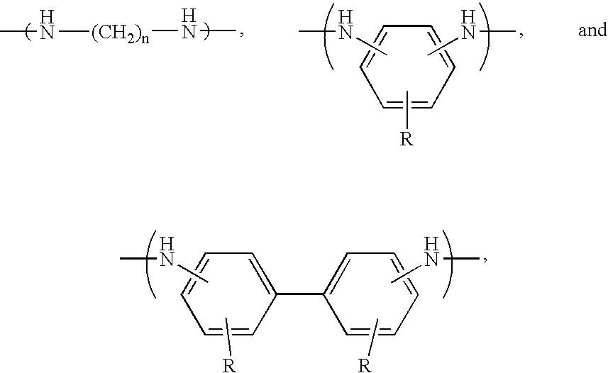
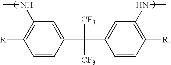
- Preferred polymers include polyesters and polyamic acids, with the preferred polyamic acids including recurring monomers having the formulas
- Preferred X and Y groups include those selected from the group consisting of substituted and unsubstituted phenyl, biphenyl, naphthyl, and anthryl groups, and substituted and unsubstituted C 1 -C 12 aliphatic (preferably alkyl) groups.
- the polyamic acids can be formed by polymerizing a dianhydride with a diamine in the presence of a solvent system and a catalyst.
- Preferred dianhydrides have the formula
- the most preferred polyamic acids for use in the present invention comprise recurring monomers selected from the group consisting of
- X is selected from the group consisting of —O—, —S—, —CH 2 —, —C(CF 3 ) 2 —, and —C(CH 3 ) 2 —;
- n 2-8;
- each R is individually selected from the group consisting of —H and —OH.
- One preferred monomer has the formula
- the polymer comprises an endcap monomer at one of its termini, and even more preferably at both of its termini.
- the endcap monomer will have a formula other than (I) or (II) above, and it will comprise functional groups that are less reactive at room temperature than the those of the other monomers within the polymer, thus reducing room temperature reactions.
- Particularly preferred endcap monomers have the formula
- Scheme A shows one example of how such an endcap monomer can be added to the polymer.
- the compositions are formed by simply dispersing or dissolving the polymers in the solvent system, preferably at ambient conditions and for a sufficient amount of time to form a substantially homogeneous dispersion.
- the polymer should be present in the composition at a level of 1-40% by weight, more preferably from about 5-25% by weight, and even more preferably from about 5-15% by weight, based upon the total weight of solids in the composition taken as 100% by weight.
- the weight average molecular weight of this polymer is preferably from about 1,000-1,000,000 Daltons, and more preferably from about 10,000-100,000 Daltons.
- Preferred solvent systems include a solvent selected from the group consisting of propylene glycol methyl ether acetate (PGMEA), propylene glycol methyl ether (PGME), ethyl lactate, and mixtures thereof.
- the solvent system should have a boiling point of from about 50-250° C., and more preferably from about 150-200° C., and should be utilized at a level of from about 80-98% by weight, preferably from about 80-95% by weight, and even more preferably from about 85-92% by weight, based upon the total weight of the composition taken as 100% by weight.
- the percent solids in the composition will be from about 2-20% by weight, preferably from about 5-20% by weight, and more preferably from about 8-15% by weight, based upon the total weight of the composition taken as 100% by weight.
- any other ingredients should be dissolved or dispersed in the solvent system along with the polymer.
- One such ingredient is a crosslinking agent.
- Preferred crosslinking agents include aminoplasts (e.g., POWDERLINK 1174, CYMEL, both from Cytec Industries), multi-functional epoxies (e.g., CY179MA from Vantico, MY720 from Ciba-Geigy), and cyanurates (triepoxy propyl isocyanurate).
- the crosslinking agent is preferably present in the composition at a level of from about 0-70% by weight, preferably from about 1-30% by weight, and more preferably from about 1-10% by weight, based upon the total weight of polymer solids in the composition taken as 100% by weight.
- the compositions of the invention should crosslink at a temperature of from about 100-250° C., and more preferably from about 150-200° C.
- the compositions also include a light attenuating compound or moiety (also referred to as a chromophore or dye).
- a light attenuating compound or moiety also referred to as a chromophore or dye.
- the light attenuating compound could be chemically attached to a polymer, or it could simply be blended into the polymer solution.
- the chemical technique to attach the light attenuating compound involves reacting the light attenuating compound (containing at least one or more pendant carboxylic acid or phenol functional groups) with an epoxy or a multifunctional epoxy compound.
- the light attenuating compound or moiety should be present in the composition at a level of from about 1-10% by weight, and preferably from about 2-6% by weight, based upon the total weight of solids in the composition taken as 100% by weight.
- the light attenuating compound is selected based upon the wavelength at which the compositions will be processed. Thus, at wavelengths of 248 nm, preferred light attenuating compounds or moieties include napthalenes and anthracenes, with 3,7-dihydroxy-2-napthoic acid being particularly preferred. At wavelengths of 193 nm, preferred light attenuating compounds or moieties include phenyl or biphenyl (aromatic or substituted aromatic rings) compounds. Particularly preferred light attenuating compounds include the following compounds (as well as functional moieties of those compounds):
- R is selected from the group consisting of cyclic (including heterocyclic rings such as cyanuric rings) and aliphatic groups.
- Aliphatic groups include both cyclic (preferably C 3 -C 12 ) and branched and unbranched alkyls (preferably C 1 -C 12 ).
- Typical optional ingredients include surfactants, catalysts, and adhesion promoters.
- the composition After application to the substrate, the composition is baked or cured.
- the baking temperatures and times affect the degree of imidization of the polyamic acid, and therefore the amount of film remaining after contacting the composition with a developer.
- the degree imidization (i.e., the conversion of polyamic acid to polyimide) after baking be at least about 20 greater, and preferably from about 30-90 greater than the degree of imidization prior to baking. This is generally accomplished by heating at a temperature of from about 130-230° C., and preferably from about 150-210° C. This heating step is preferably carried out for a time period of from about 30-120 seconds, and more preferably from about 45-90 seconds.
- the developer is preferably a commercially available aqueous developer comprising a base.
- Particularly preferred developers include those selected from the group consisting of tetramethyl ammonium hydroxide, potassium hydroxide, sodium hydroxide, and mixtures thereof.
- the developer is preferably allowed to contact the layer for a time period of from about 30-90 seconds, more preferably from about 45-80 seconds, and even more preferably for about 55-65 seconds.
- the developer is then removed from the substrate, preferably by spinning at a speed of from about 1,500-2,500 rpm for a time period of from about 20-40 seconds.
- the developer contact step results in the composition being at least partially removed.
- the developer contact step removes or recesses the composition at a rate of from about 1-500 ⁇ of thickness per second of developer contact, more preferably from about 10-300 ⁇ of thickness per second of developer contact, and even more preferably from about 20-200 ⁇ of thickness per second of developer contact.
- the amount of recess can be to a level above, at, or below the upper edge of the vias, depending upon the application. If the material is recessed to a point above the upper edge of the vias, the remaining film can be used as an anti-reflective layer at its first or second reflective minimum thickness.
- the material is recessed to a level at or below the upper edge of the vias, the material will act only as a gap-filling material, and another anti-reflective coating layer is preferably applied to suppress light reflecting from the substrate.
- Having the material recessed to partially fill the vias can be advantageous because less bottom anti-reflective coating must be etched. Minimization of the material that must be etched in the vias results in reduced fencing or crown formation after trench etch.
- fences or crowns are bottom anti-reflective coating or dielectric residue that remains after the trench etch because of poor etch selectivity between the via-fill, bottom anti-reflective coating and the interlayer dielectric.
- the inventive process can be used in both partial fill (i.e., where about 35-65% of the hole's depth is filled with the composition) and full-fill (i.e., where at least about 95%, and preferably about 100% of the hole's depth is filled with the composition) applications.
- the inventive methods can be used to form dual damascene structures possessing properties not previously achieved.
- the structures prepared according to the inventive methods will have low biases, even with very thin layers of the composition.
- the inventive methods will result in layers having biases of less than about 20 nm, preferably less than about 10 nm, and more preferably from about 0-5 nm, even at average film thicknesses of less than about 200 nm.
- the average thickness of a layer is determined by measuring (with an ellipsometer or other conventional device) the thickness of a layer at a point about halfway between two via holes: (1) that are not separated from one another by an intervening feature; and (2) whose boundaries are within 1,000 nm of one another. These measurements are repeated over a wafer (or other area as defined herein) up to 49 times, and the measurements are averaged to determine the average thickness of a layer.
- the bias is determined by subtracting the average thickness of a layer over a dense region from the average thickness of that same layer over an isolated region.
- a dense region is defined as a portion of a substrate that has at least about 50% of its surface area filled with via holes, while an isolated region is defined as a portion of a substrate that has less than about 20% of its surface area filled with via holes.
- a photoresist layer can then be applied to the recessed composition (or to an anti-reflective coating applied on the recessed composition), with the photoresist layer being patterned according to conventional processes (e.g., exposure to activating radiation at the wavelength of interest, developing the exposed photoresist). Since the inventive method is particularly well-suited for via first methods, this patterning step will typically involve patterning the desired trenches, follow by etching (e.g., plasm etching) of those trenches into the substrate. It will be appreciated that this method is particularly advantageous over the prior art because it is compatible with copper-containing circuits, while avoiding the issues typically encountered with methods where etching of copper is required.
- FIG. 1 is a schematic drawing showing prior art, via-first, dual damascene layers using a gap-fill material without light-absorbing properties;
- FIG. 2 is a schematic drawing illustrating the gap-fill properties of prior art organic bottom anti-reflective coatings.
- FIG. 3 is a scanning electron microscope (SEM) photograph showing the different recess levels used with the inventive method described in Example 1.
- a polymer mother liquor and a dye solution were first prepared.
- the polymer mother liquor was prepared by mixing, in the order listed, the following reagents:
- the Bis-AP-AF and the HAB were added to a 1-liter, round-bottom flask.
- the 500 g of PGME were added to the diamines.
- the mixture was stirred until all of the Bis-AP-AF was in solution, and the HAB was broken into a fine, suspended powder.
- the mixture was then heated to 60° C. using a silicone oil bath.
- the PMDA was added, and the addition funnel and flask walls were rinsed with the remaining PGME.
- the flask was then sealed, and the monomers were allowed to react for 24 hours in a nitrogen atmosphere. After 24 hours, the polymer solution was cooled to room temperature, filtered through a 0.45- ⁇ m endpoint filter, and bottled in a 1-liter Nalgene® bottle.
- the dye solution was prepared by mixing the following reagents in a 250-ml flask:
- composition of this example was made by mixing the following ingredients together:
- the total weight of the composition mixture was 130.86 g, with 8% solids.
- the composition was spin applied at 1,500 rpm for 60 seconds onto silicon wafers and then baked at 175° C. for 60 seconds using a proximity bake plate.
- the film thickness of the coating was measured using an ellipsometer. The thickness range was from 290 to 300 nm across a 200-mm silicon wafer.
- the optical properties (n and k values) were determined using a J. A. Woollam variable angle spectroscopic ellipsometer (VASE).
- This composition was also spin applied on substrates having via holes ranging in size from 0.1 to 0.3 ⁇ m.
- the composition was spun on at 1,000 rpm for 10 seconds followed by 1,500 rpm for 30 to 50 seconds.
- the film was then baked on a proximity hotplate at a temperature of 180° C. for a time period of 60 seconds.
- the via holes were completely planarized after the composition was spin coated onto the substrate.
- the thickness of the composition ranged from 100 nm to 600 nm depending on the size and density of via holes present on the substrate.
- a standard 0.26N TMAH developer was puddled on the substrate for 60 seconds and then spun off. The wafer was then rinsed with deionized water, and the wafer was baked at 100° C. for 10 seconds to remove any residual water from the surface of the substrate.
- FIG. 3 shows a set of examples using the composition of this example where the substrate contained via holes that were 0.25 ⁇ m in diameter and 0.7 ⁇ m deep.
- FIG. 3( a ) shows a sample prior to the wet recess process.
- FIG. 3( b ) shows a sample that was baked at 180° C. for 60 seconds, followed by recessing of the composition to the second reflectivity minimum thickness of the composition.
- FIG. 3( c ) shows a sample that was baked at 180° C. for 60 seconds, followed by recessing for 60 seconds to the via surface.
- FIG. 3( d ) shows a sample that was baked at 140° C. for 60 seconds, followed by recessing for 30 seconds so that the composition was recessed to below the upper edge of the via holes (for partial fill).
- This composition was prepared by mixing the following ingredients:
- the total weight of composition was 57.0 g, with 8% solids.
- composition was then spin coated, processed, and examined using the same methods described in Example 1.
- a proximity bake plate was used to bake the wafers.
- This composition was prepared by mixing the following ingredients:
- the total weight of the composition was 38.0 g, with 8% solids.
- composition was then spin coated, processed, and examined using the same methods described in Example 1.
- a proximity bake plate was used to bake the wafers.
- Tables I sets forth the n and k values at 193- and 248-nm wavelengths for the compositions described in Examples 1-3 above.
- a dye solution was prepared by adding the following reagents to a 100-ml, 3-neck, round-bottom flask equipped with nitrogen inlet, thermometer, condenser, and a stir bar:
- the reaction flask was immersed in an oil bath heated to 120° C. The reaction was stirred for 24 hours at reflux.
- Two formulations were prepared—one including the dye solution and one without the dye solution.
- the formulation without the dye solution was prepared by blending the following ingredients to form a homogeneous solution:
- This formulation was spin applied at 1,500 rpm for 60 seconds onto a silicon wafer containing via holes.
- the formulation including the dye solution was prepared by blending the following ingredients to form a homogeneous solution:
- This formulation was spin applied at 1,500 rpm for 60 seconds onto a silicon wafer containing via holes.
- the flask was then immersed in an oil bath maintained at 60° C.
- a water condenser was attached to the flask, and the contents of the flask were stirred using a magnetic stirrer.
- the reagents were stirred and then filtered through a 0.1- ⁇ m endpoint filter.
- the reagents were stirred and then filtered through a 0.1- ⁇ m endpoint filter.
- the reagents were stirred and then filtered through a 0.1- ⁇ m endpoint filter.
- the reagents were stirred and then filtered through a 0.1- ⁇ m endpoint filter.
- the flask was then immersed in an oil bath maintained at 60° C. A water condenser was attached, and the contents of the flask were stirred using a magnetic stirrer. After complete dissolution of the Bis-AP-AF, 3.0 g (0.0137 mole) of pyromellitic dianhydride were added to the solution. The reaction was allowed to stir for 18 hours, and then 4.07 g (0.0275 mole) of phthalic anhydride were added. The reaction was stirred at 60° C. for 3 hours and cooled to ambient temperature.
- the reagents were stirred and then filtered through a 0.1- ⁇ m endpoint filter.
Abstract
Description

Preferred X and Y groups include those selected from the group consisting of substituted and unsubstituted phenyl, biphenyl, naphthyl, and anthryl groups, and substituted and unsubstituted C1-C12 aliphatic (preferably alkyl) groups.

while preferred diamines have the formula
where X and Y are as defined above.

where:


where R is selected from the group consisting of cyclic (including heterocyclic rings such as cyanuric rings) and aliphatic groups. Aliphatic groups include both cyclic (preferably C3-C12) and branched and unbranched alkyls (preferably C1-C12).
-
- 39.46 g of 2,2-bis(3-amino-4-hydroxyphenyl) hexafluoropropane (Bis-AP-AF; obtained from ChrisKev Corp.);
- 1.24 g of 3,3′-dihydroxy-4,4′-aminobenzidine (HAB; obtained from ChrisKev Corp.);
- 500 g of propylene glycol monomethyl ether (PGME; obtained from Harcross Corp.);
- 25 g of pyromellitic dianhydride (PMDA; obtained from ChrisKev Corp.); and
- 91.3 g of PGME.

-
- 7.25 g of triglycidyl epoxy propyl cyanurate (TEPIC; obtained from Aldrich Chemical Corp.);
- 13.33 g of 3,7-dihydroxy napthoic acid (obtained from Aldrich Chemical Corp.);
- 7.25 g of 9-anthracene carboxylic acid (obtained from TCI Chemicals Ltd.);
- 0.56 g of benzyl triethyl ammonium chloride (BTEAC; obtained from Aldrich Chemical Corp.); and
- 122.32 g of PGME.
-
- 55.0 g of the polymer solution prepared above (5.5 g polymer solids and 49.5 g PGME);
- 16.5 g of the dye solution prepared above (3.3 g dye solids and 13.2 g PGME);
- 1.67 g of MY720 (Ciba-Geigy);
- 21.57 g of PGME; and
- 36.12 g of PGMEA.
-
- 24.0 g of the polymer solution prepared above (2.4 g of polymer solids, 21.6 g of PGME);
- 7.20 g of dye solution (1.44 g of solids, 5.76 g of PGME);
- 0.72 g of triepoxy propyl cyanurate (30% of polymer solids);
- 9.34 g of PGME; and
- 15.73 g of PGMEA.
-
- 12.0 g of the polymer solution prepared above (1.2 g of polymer solids, 10.8 g of PGME);
- 7.20 g of the dye solution prepared above (1.44 g of solids, 5.76 g of PGME);
- 0.4 g of CY179MA (33% of polymer solids; obtained from Vantico);
- 7.64 g of PGME; and
- 10.76 g of PGMEA.
| TABLE I | ||||
| Example | n (193 nm) | k (193 nm) | n (248 nm) | k (248 nm) |
| 1 | 1.45 | 0.45 | 1.76 | 0.42 |
| 2 | 1.46 | 0.47 | 1.73 | 0.4 |
| 3 | 1.45 | 0.44 | 1.75 | 0.43 |
-
- 9.61 g of citric acid (obtained from Aldrich);
- 13.91 g of EX721 (obtained from Nagase Chemicals);
- 0.68 g of tetrabutylphosphonium bromide (obtained from Aldrich); and
- 96.80 g of PGME.
-
- 14.29 g of TEPIC (obtained from Nissan Chemical Industries);
- 25.52 g of 3,7-dihydroxynaphthoic acid (obtained from Aldrich);
- 0.214 g of imidazole (obtained Aldrich); and
- 59.98 g of PGME.
-
- 10.0 g of the polymer mother liquor described in this example;
- 1.4 g of N,N-diglycidyl-4-glycidyloxyanaline (obtained from Aldrich);
- 3.45 g of PGME; and
- 12.15 g of propylene glycol propyl ether (PnP; obtained from Harcross).
-
- 10.0 g of the polymer mother liquor described in this example;
- 1.4 g of N,N-diglycidyl-4-glycidyloxyanaline;
- 3.75 g of the dye solution described in this example;
- 3.45 g of PGME; and
- 12.15 g of PnP.
-
- 22.35 g (0.0611 mole) of Bis-AP-AF; and
- 96.96 g of PGME.
-
- 15 g of the polymer mother liquor prepared in this example;
- 3.55 g of crosslinker CY179MA;
- 28.56 g of PGME; and
- 16.90 g of PGMEA.
-
- 36.30 g of the polymer mother liquor prepared in this example;
- 4.00 g of crosslinker MY720 (50% weight solution in PGME);
- 33.30 g of PGME; and
- 26.40 g of PGMEA.
-
- 36.30 g of the polymer mother liquor prepared in this example;
- 4.00 g of crosslinker DEN 438 (obtained from Araldite; 50% weight solution in PGME);
- 33.30 g of PGME; and
- 26.40 g of PGMEA.
-
- 10 g of the polymer mother liquor prepared in this example;
- 1.08 g of crosslinker MY720 (50% weight solution in PGME);
- 0.54 g of trishydroxyphenyl ethane;
- 11.56 g of PGME; and
- 8.316 of PGMEA.
-
- 10.0 g (0.0275 mole) of Bis-AP-AF; and
- 96.96 g of PGME.
-
- 36.30 g of the polymer mother liquor prepared in this example;
- 4.00 g of crosslinker MY720 (50% weight solution in PGME);
- 33.30 g of PGME; and
- 26.40 g of PGMEA.
Claims (36)


Priority Applications (5)
| Application Number | Priority Date | Filing Date | Title |
|---|---|---|---|
| US10/966,909 US7364835B2 (en) | 2003-10-15 | 2004-10-15 | Developer-soluble materials and methods of using the same in via-first dual damascene applications |
| PCT/US2004/034495 WO2005038878A2 (en) | 2003-10-15 | 2004-10-15 | Developer-soluble materials and methods of using the same in via-first dual damascene applications |
| EP04795633.9A EP1673801B1 (en) | 2003-10-15 | 2004-10-15 | Developer-soluble materials and methods of using the same in via-first dual damascene applications |
| JP2006535432A JP5368674B2 (en) | 2003-10-15 | 2004-10-15 | Method for using developer-soluble material and developer-soluble material in via-first dual damascene application |
| KR1020067007008A KR101189397B1 (en) | 2003-10-15 | 2004-10-15 | Developer-soluble materials and methods of using the same in via-first dual damascene applications |
Applications Claiming Priority (2)
| Application Number | Priority Date | Filing Date | Title |
|---|---|---|---|
| US51176203P | 2003-10-15 | 2003-10-15 | |
| US10/966,909 US7364835B2 (en) | 2003-10-15 | 2004-10-15 | Developer-soluble materials and methods of using the same in via-first dual damascene applications |
Publications (2)
| Publication Number | Publication Date |
|---|---|
| US20050148170A1 US20050148170A1 (en) | 2005-07-07 |
| US7364835B2 true US7364835B2 (en) | 2008-04-29 |
Family
ID=34468002
Family Applications (1)
| Application Number | Title | Priority Date | Filing Date |
|---|---|---|---|
| US10/966,909 Active 2025-03-26 US7364835B2 (en) | 2003-10-15 | 2004-10-15 | Developer-soluble materials and methods of using the same in via-first dual damascene applications |
Country Status (5)
| Country | Link |
|---|---|
| US (1) | US7364835B2 (en) |
| EP (1) | EP1673801B1 (en) |
| JP (1) | JP5368674B2 (en) |
| KR (1) | KR101189397B1 (en) |
| WO (1) | WO2005038878A2 (en) |
Cited By (9)
| Publication number | Priority date | Publication date | Assignee | Title |
|---|---|---|---|---|
| US20090035590A1 (en) * | 2007-07-30 | 2009-02-05 | Sullivan Daniel M | Non-covalently crosslinkable materials for photolithography processes |
| US20090325106A1 (en) * | 2008-06-27 | 2009-12-31 | Conley Willard E | Method for Implant Imaging with Spin-on Hard Masks |
| US20120034419A1 (en) * | 2010-08-05 | 2012-02-09 | Brewer Science Inc. | Methods of producing structures using a developer-soluble layer with multilayer technology |
| WO2013055798A1 (en) | 2011-10-10 | 2013-04-18 | Brewer Science Inc. | Spin-on carbon compositions for lithographic processing |
| CN104749880A (en) * | 2013-12-31 | 2015-07-01 | 三星Sdi株式会社 | Hardmask Composition And Method Of Forming Patterns By Using The Hardmask Composition |
| US9121237B2 (en) | 2011-07-28 | 2015-09-01 | Baker Hughes Incorporated | Methods of coating wellbore tools and components having such coatings |
| CN105093834A (en) * | 2014-05-16 | 2015-11-25 | 三星Sdi株式会社 | Hardmask composition and method of forming patterns using the hardmask composition |
| US9874812B2 (en) | 2015-01-30 | 2018-01-23 | Samsung Electronics Co., Ltd. | Methods of forming hardmask material film |
| US9960038B2 (en) | 2010-12-27 | 2018-05-01 | Brewer Science, Inc. | Processes to pattern small features for advanced patterning needs |
Families Citing this family (13)
| Publication number | Priority date | Publication date | Assignee | Title |
|---|---|---|---|---|
| US20070207406A1 (en) * | 2004-04-29 | 2007-09-06 | Guerrero Douglas J | Anti-reflective coatings using vinyl ether crosslinkers |
| US20050255410A1 (en) * | 2004-04-29 | 2005-11-17 | Guerrero Douglas J | Anti-reflective coatings using vinyl ether crosslinkers |
| US20060216929A1 (en) * | 2005-03-28 | 2006-09-28 | Hyun-Mog Park | Etch stopless dual damascene structure and method of fabrication |
| KR100703007B1 (en) * | 2005-11-17 | 2007-04-06 | 삼성전자주식회사 | Composition for forming an organic anti-reflective coating layer of photo sensitivity and method of forming a pattern using the same |
| US7914974B2 (en) | 2006-08-18 | 2011-03-29 | Brewer Science Inc. | Anti-reflective imaging layer for multiple patterning process |
| US7862986B2 (en) * | 2007-10-17 | 2011-01-04 | Macronix International Co., Ltd. | Patterning process |
| US8133659B2 (en) | 2008-01-29 | 2012-03-13 | Brewer Science Inc. | On-track process for patterning hardmask by multiple dark field exposures |
| US9640396B2 (en) | 2009-01-07 | 2017-05-02 | Brewer Science Inc. | Spin-on spacer materials for double- and triple-patterning lithography |
| JP5888523B2 (en) * | 2011-03-15 | 2016-03-22 | 日産化学工業株式会社 | Resist underlayer film forming composition and resist pattern forming method using the same |
| WO2013141015A1 (en) * | 2012-03-23 | 2013-09-26 | 日産化学工業株式会社 | Composition for forming resist lower layer film for euv lithography |
| CN104303107B (en) * | 2012-05-07 | 2016-07-27 | 日产化学工业株式会社 | For forming the compositions of resist lower membrane |
| KR102011446B1 (en) * | 2013-02-26 | 2019-10-14 | 삼성전자주식회사 | Method of forming thin layer patterns in semiconductor device |
| US11022886B2 (en) * | 2017-05-17 | 2021-06-01 | Taiwan Semiconductor Manufacturing Co,, Ltd. | Bottom-up material formation for planarization |
Citations (99)
| Publication number | Priority date | Publication date | Assignee | Title |
|---|---|---|---|---|
| US3615615A (en) | 1970-04-13 | 1971-10-26 | Eastman Kodak Co | Photographic emulsions including reactive quaternary salts |
| JPS48891U (en) | 1971-05-26 | 1973-01-08 | ||
| US3856751A (en) | 1972-06-14 | 1974-12-24 | Eastman Kodak Co | Diacid-xanthylium ion polyester and photographic element comprised thereof |
| US4175175A (en) | 1963-07-16 | 1979-11-20 | Union Carbide Corporation | Polyarylene polyethers |
| US4244799A (en) | 1978-09-11 | 1981-01-13 | Bell Telephone Laboratories, Incorporated | Fabrication of integrated circuits utilizing thick high-resolution patterns |
| US4320224A (en) | 1977-09-07 | 1982-03-16 | Imperial Chemical Industries Limited | Thermoplastic aromatic polyetherketones |
| US4369090A (en) | 1980-11-06 | 1983-01-18 | Texas Instruments Incorporated | Process for etching sloped vias in polyimide insulators |
| US4683024A (en) | 1985-02-04 | 1987-07-28 | American Telephone And Telegraph Company, At&T Bell Laboratories | Device fabrication method using spin-on glass resins |
| US4732841A (en) | 1986-03-24 | 1988-03-22 | Fairchild Semiconductor Corporation | Tri-level resist process for fine resolution photolithography |
| US4738916A (en) | 1984-06-11 | 1988-04-19 | Nippon Telegraph And Telephone Corp. | Intermediate layer material of three-layer resist system |
| US4742152A (en) | 1986-05-27 | 1988-05-03 | United Technologies Corporation | High temperature fluorinated polyimides |
| US4803147A (en) | 1987-11-24 | 1989-02-07 | Hoechst Celanese Corporation | Photosensitive polyimide polymer compositions |
| US4891303A (en) | 1988-05-26 | 1990-01-02 | Texas Instruments Incorporated | Trilayer microlithographic process using a silicon-based resist as the middle layer |
| US4910122A (en) | 1982-09-30 | 1990-03-20 | Brewer Science, Inc. | Anti-reflective coating |
| US4927736A (en) | 1987-07-21 | 1990-05-22 | Hoechst Celanese Corporation | Hydroxy polyimides and high temperature positive photoresists therefrom |
| US4996247A (en) | 1984-02-10 | 1991-02-26 | General Electric Company | Enhancing color stability to sterilizing radiation of polymer compositions |
| US5057399A (en) | 1989-03-31 | 1991-10-15 | Tony Flaim | Method for making polyimide microlithographic compositions soluble in alkaline media |
| US5089593A (en) | 1988-06-28 | 1992-02-18 | Amoco Corporation | Polyimide containing 4,4'-bis(4-amino-2-trifluoromethylphenoxy)-biphenyl moieties |
| US5091047A (en) | 1986-09-11 | 1992-02-25 | National Semiconductor Corp. | Plasma etching using a bilayer mask |
| US5106718A (en) | 1988-10-20 | 1992-04-21 | Ciba-Geigy Corporation | Positive photoresist composition containing alkali-soluble phenolic resin, photosensitive quinonediazide compound and sulfonyl containing compound |
| US5126231A (en) | 1990-02-26 | 1992-06-30 | Applied Materials, Inc. | Process for multi-layer photoresist etching with minimal feature undercut and unchanging photoresist load during etch |
| US5304626A (en) | 1988-06-28 | 1994-04-19 | Amoco Corporation | Polyimide copolymers containing 3,3',4,4'-tetracarboxybiphenyl dianhydride (BPDA) moieties |
| US5370969A (en) | 1992-07-28 | 1994-12-06 | Sharp Kabushiki Kaisha | Trilayer lithographic process |
| US5397684A (en) | 1993-04-27 | 1995-03-14 | International Business Machines Corporation | Antireflective polyimide dielectric for photolithography |
| US5403438A (en) | 1991-01-10 | 1995-04-04 | Fujitsu Limited | Process for forming pattern |
| GB2288184A (en) | 1994-03-31 | 1995-10-11 | Catalysts & Chem Ind Co | Coating composition |
| US5542971A (en) | 1994-12-01 | 1996-08-06 | Pitney Bowes | Bar codes using luminescent invisible inks |
| US5554473A (en) | 1994-11-23 | 1996-09-10 | Mitsubishi Chemical America, Inc. | Photoreceptor having charge transport layers containing a copolycarbonate and layer containing same |
| US5607824A (en) | 1994-07-27 | 1997-03-04 | International Business Machines Corporation | Antireflective coating for microlithography |
| US5632910A (en) | 1993-12-24 | 1997-05-27 | Sony Corporation | Multilayer resist pattern forming method |
| US5688987A (en) | 1994-11-09 | 1997-11-18 | Brewer Science, Inc. | Non-subliming Mid-UV dyes and ultra-thin organic arcs having differential solubility |
| US5691101A (en) | 1994-03-15 | 1997-11-25 | Kabushiki Kaisha Toshiba | Photosensitive composition |
| US5739254A (en) | 1996-08-29 | 1998-04-14 | Xerox Corporation | Process for haloalkylation of high performance polymers |
| JPH10149531A (en) | 1996-11-15 | 1998-06-02 | Sony Corp | Magnetic recording medium and its production |
| US5772925A (en) | 1994-06-29 | 1998-06-30 | Shin-Etsu Chemical Co., Ltd. | Anti-reflective coating composition |
| JPH10307394A (en) | 1997-05-09 | 1998-11-17 | Hitachi Ltd | Positive photosensitive resin composition and pattern forming method by using the same and method of manufacture of electronic device |
| US5925578A (en) | 1995-12-29 | 1999-07-20 | Hyundai Electronics Industries Co., Ltd. | Method for forming fine patterns of a semiconductor device |
| US5952448A (en) | 1996-12-31 | 1999-09-14 | Korea Research Institute Of Chemical Technology | Stable precursor of polyimide and a process for preparing the same |
| US5998569A (en) | 1998-03-17 | 1999-12-07 | International Business Machines Corporation | Environmentally stable optical filter materials |
| US6015650A (en) | 1995-12-29 | 2000-01-18 | Hyundai Electronics Industries Co., Ltd. | Method for forming micro patterns of semiconductor devices |
| US6020269A (en) | 1998-12-02 | 2000-02-01 | Advanced Micro Devices, Inc. | Ultra-thin resist and nitride/oxide hard mask for metal etch |
| US6046112A (en) * | 1998-12-14 | 2000-04-04 | Taiwan Semiconductor Manufacturing Company | Chemical mechanical polishing slurry |
| US6054254A (en) | 1997-07-03 | 2000-04-25 | Kabushiki Kaisha Toshiba | Composition for underlying film and method of forming a pattern using the film |
| US6071662A (en) | 1998-07-23 | 2000-06-06 | Xerox Corporation | Imaging member with improved anti-curl backing layer |
| US6110653A (en) | 1999-07-26 | 2000-08-29 | International Business Machines Corporation | Acid sensitive ARC and method of use |
| US6127070A (en) | 1998-12-01 | 2000-10-03 | Advanced Micro Devices, Inc. | Thin resist with nitride hard mask for via etch application |
| US6136679A (en) | 1999-03-05 | 2000-10-24 | Taiwan Semiconductor Manufacturing Company | Gate micro-patterning process |
| US6136511A (en) | 1999-01-20 | 2000-10-24 | Micron Technology, Inc. | Method of patterning substrates using multilayer resist processing |
| US6156658A (en) | 1998-12-02 | 2000-12-05 | Advanced Micro Devices, Inc. | Ultra-thin resist and silicon/oxide hard mask for metal etch |
| US6156665A (en) | 1998-04-13 | 2000-12-05 | Lucent Technologies Inc. | Trilayer lift-off process for semiconductor device metallization |
| US6165695A (en) | 1998-12-01 | 2000-12-26 | Advanced Micro Devices, Inc. | Thin resist with amorphous silicon hard mask for via etch application |
| US6171763B1 (en) | 1998-12-02 | 2001-01-09 | Advanced Micro Devices, Inc. | Ultra-thin resist and oxide/nitride hard mask for metal etch |
| US6200907B1 (en) | 1998-12-02 | 2001-03-13 | Advanced Micro Devices, Inc. | Ultra-thin resist and barrier metal/oxide hard mask for metal etch |
| US6218292B1 (en) | 1997-12-18 | 2001-04-17 | Advanced Micro Devices, Inc. | Dual layer bottom anti-reflective coating |
| US6251562B1 (en) | 1998-12-23 | 2001-06-26 | International Business Machines Corporation | Antireflective polymer and method of use |
| US6306560B1 (en) | 1998-12-02 | 2001-10-23 | Advanced Micro Devices, Inc. | Ultra-thin resist and SiON/oxide hard mask for metal etch |
| US6309789B1 (en) | 1998-06-03 | 2001-10-30 | Clariant Finance (Bvi) Limited | Composition for reflection reducing coating |
| US6309926B1 (en) | 1998-12-04 | 2001-10-30 | Advanced Micro Devices | Thin resist with nitride hard mask for gate etch application |
| US6319649B1 (en) | 1994-10-13 | 2001-11-20 | Hitachi, Ltd. | Photosensitive resin composition and method of forming resist images |
| US6338936B1 (en) | 1998-02-02 | 2002-01-15 | Taiyo Ink Manufacturing Co., Ltd. | Photosensitive resin composition and method for formation of resist pattern by use thereof |
| US20020009599A1 (en) | 2000-01-26 | 2002-01-24 | Welch Cletus N. | Photochromic polyurethane coating and articles having such a coating |
| US6359028B1 (en) | 1995-07-12 | 2002-03-19 | Mitsubishi Engineering-Plastics Corporation | Polycarbonate resin composition |
| US6361833B1 (en) | 1998-10-28 | 2002-03-26 | Henkel Corporation | Composition and process for treating metal surfaces |
| US6380611B1 (en) | 1998-09-03 | 2002-04-30 | Micron Technology, Inc. | Treatment for film surface to reduce photo footing |
| US6391472B1 (en) | 1999-08-26 | 2002-05-21 | Brewer Science, Inc. | Fill material for dual damascene processes |
| US6440640B1 (en) | 1998-12-01 | 2002-08-27 | Advanced Micro Devices, Inc. | Thin resist with transition metal hard mask for via etch application |
| US6451498B1 (en) | 1998-05-28 | 2002-09-17 | Atotech Deutschland Gmbh | Photosensitive composition |
| US6455416B1 (en) * | 2000-10-24 | 2002-09-24 | Advanced Micro Devices, Inc. | Developer soluble dyed BARC for dual damascene process |
| US6458705B1 (en) | 2001-06-06 | 2002-10-01 | United Microelectronics Corp. | Method for forming via-first dual damascene interconnect structure |
| US6488509B1 (en) | 2002-01-23 | 2002-12-03 | Taiwan Semiconductor Manufacturing Company | Plug filling for dual-damascene process |
| US6487879B1 (en) | 1997-03-07 | 2002-12-03 | Corning Incorporated | Method of making titania-doped fused silica |
| US6509137B1 (en) | 2000-02-10 | 2003-01-21 | Winbond Electronics Corp. | Multilayer photoresist process in photolithography |
| US20030040179A1 (en) | 2001-08-24 | 2003-02-27 | Thakar Gautam V. | Polysilicon processing using an anti-reflective dual layer hardmask for 193 nm lithography |
| US6586560B1 (en) | 2001-09-18 | 2003-07-01 | Microchem Corp. | Alkaline soluble maleimide-containing polymers |
| JP2003183387A (en) * | 2001-12-19 | 2003-07-03 | Central Glass Co Ltd | Fluorine-containing alicylic diamine and polymer using the same |
| US20030122269A1 (en) | 2001-05-29 | 2003-07-03 | Essilor International Compagnie Generale D'optique | Method for forming on-site a coated optical article |
| US20030129531A1 (en) | 2002-01-09 | 2003-07-10 | Oberlander Joseph E. | Positive-working photoimageable bottom antireflective coating |
| US20030129547A1 (en) | 2002-01-09 | 2003-07-10 | Neisser Mark O. | Process for producing an image using a first minimum bottom antireflective coating composition |
| US20030143404A1 (en) | 2001-11-01 | 2003-07-31 | Welch Cletus N. | Articles having a photochromic polymeric coating |
| US20030166828A1 (en) | 2002-01-17 | 2003-09-04 | Brewer Science, Inc. | Spin bowl compatible polyamic acids/imides as wet developable polymer binders for anti-reflective coatings |
| US20030194636A1 (en) | 2002-04-11 | 2003-10-16 | Wanat Stanley F. | Photoresist compositions comprising acetals and ketals as solvents |
| US6638853B1 (en) * | 2002-07-03 | 2003-10-28 | Taiwan Semiconductor Manufacturing Co. Ltd. | Method for avoiding photoresist resist residue on semioconductor feature sidewalls |
| US20030215736A1 (en) | 2002-01-09 | 2003-11-20 | Oberlander Joseph E. | Negative-working photoimageable bottom antireflective coating |
| US6680252B2 (en) * | 2001-05-15 | 2004-01-20 | United Microelectronics Corp. | Method for planarizing barc layer in dual damascene process |
| US20040018451A1 (en) | 2002-07-23 | 2004-01-29 | Samsung Electronics Co., Ltd. | Photoresist developer-soluble organic bottom antireflective composition and photolithography and etching process using the same |
| US6709979B2 (en) * | 2000-05-29 | 2004-03-23 | Sony Corporation | Method of manufacturing a semiconductor device |
| US20040058275A1 (en) | 2002-06-25 | 2004-03-25 | Brewer Science, Inc. | Wet-developable anti-reflective compositions |
| US20040077173A1 (en) | 2002-10-17 | 2004-04-22 | Swaminathan Sivakumar | Using water soluble bottom anti-reflective coating |
| US6740469B2 (en) | 2002-06-25 | 2004-05-25 | Brewer Science Inc. | Developer-soluble metal alkoxide coatings for microelectronic applications |
| US20040219456A1 (en) | 2002-07-31 | 2004-11-04 | Guerrero Douglas J. | Photosensitive bottom anti-reflective coatings |
| US20040220379A1 (en) * | 2003-05-02 | 2004-11-04 | Park Seung Koo | Polyamic ester having moieties of electro optic and nonlinear optical compound in side chains as an electro optic and nonlinear optical polymer, manufacturing method therefor and film manufactured therefrom |
| WO2004113417A1 (en) | 2003-05-23 | 2004-12-29 | Dow Corning Corporation | Siloxane resin-based anti-reflective coating composition having high wet etch rate |
| US6838223B2 (en) | 2002-02-16 | 2005-01-04 | Samsung Electronics Co., Ltd. | Compositions for anti-reflective light absorbing layer and method for forming patterns in semiconductor device using the same |
| US6849293B2 (en) * | 2002-05-02 | 2005-02-01 | Institute Of Microelectronics | Method to minimize iso-dense contact or via gap filling variation of polymeric materials in the spin coat process |
| US20050074699A1 (en) | 2003-06-11 | 2005-04-07 | Sun Sam X. | Wet developable hard mask in conjunction with thin photoresist for micro photolithography |
| US6893702B2 (en) * | 2000-05-29 | 2005-05-17 | Fujitsu Limited | Magnetic recording medium substrate, method of producing the same, and method of evaluating magnetic recording medium |
| US6924228B2 (en) * | 2003-03-06 | 2005-08-02 | Samsung Electronics Co., Ltd. | Method of forming a via contact structure using a dual damascene technique |
| US6976904B2 (en) * | 1998-07-09 | 2005-12-20 | Li Family Holdings, Ltd. | Chemical mechanical polishing slurry |
| US7265431B2 (en) | 2002-05-17 | 2007-09-04 | Intel Corporation | Imageable bottom anti-reflective coating for high resolution lithography |
Family Cites Families (4)
| Publication number | Priority date | Publication date | Assignee | Title |
|---|---|---|---|---|
| JP3039467B2 (en) * | 1997-07-31 | 2000-05-08 | 日本電気株式会社 | Resist development method |
| KR100416596B1 (en) * | 2001-05-10 | 2004-02-05 | 삼성전자주식회사 | Method of manufacturing interconnection wire in semiconductor device |
| US6670425B2 (en) * | 2001-06-05 | 2003-12-30 | Brewer Science, Inc. | Anti-reflective coating of polymer with epoxide rings reacted with light attenuating compound and unreacted epoxide rings |
| JP3708472B2 (en) * | 2001-10-12 | 2005-10-19 | 東京応化工業株式会社 | Resist pattern forming method and semiconductor device manufacturing method |
-
2004
- 2004-10-15 EP EP04795633.9A patent/EP1673801B1/en not_active Not-in-force
- 2004-10-15 WO PCT/US2004/034495 patent/WO2005038878A2/en active Search and Examination
- 2004-10-15 JP JP2006535432A patent/JP5368674B2/en active Active
- 2004-10-15 US US10/966,909 patent/US7364835B2/en active Active
- 2004-10-15 KR KR1020067007008A patent/KR101189397B1/en active IP Right Grant
Patent Citations (106)
| Publication number | Priority date | Publication date | Assignee | Title |
|---|---|---|---|---|
| US4175175A (en) | 1963-07-16 | 1979-11-20 | Union Carbide Corporation | Polyarylene polyethers |
| US3615615A (en) | 1970-04-13 | 1971-10-26 | Eastman Kodak Co | Photographic emulsions including reactive quaternary salts |
| JPS48891U (en) | 1971-05-26 | 1973-01-08 | ||
| US3856751A (en) | 1972-06-14 | 1974-12-24 | Eastman Kodak Co | Diacid-xanthylium ion polyester and photographic element comprised thereof |
| US4320224A (en) | 1977-09-07 | 1982-03-16 | Imperial Chemical Industries Limited | Thermoplastic aromatic polyetherketones |
| US4244799A (en) | 1978-09-11 | 1981-01-13 | Bell Telephone Laboratories, Incorporated | Fabrication of integrated circuits utilizing thick high-resolution patterns |
| US4369090A (en) | 1980-11-06 | 1983-01-18 | Texas Instruments Incorporated | Process for etching sloped vias in polyimide insulators |
| US4910122A (en) | 1982-09-30 | 1990-03-20 | Brewer Science, Inc. | Anti-reflective coating |
| US4996247A (en) | 1984-02-10 | 1991-02-26 | General Electric Company | Enhancing color stability to sterilizing radiation of polymer compositions |
| US4738916A (en) | 1984-06-11 | 1988-04-19 | Nippon Telegraph And Telephone Corp. | Intermediate layer material of three-layer resist system |
| US4683024A (en) | 1985-02-04 | 1987-07-28 | American Telephone And Telegraph Company, At&T Bell Laboratories | Device fabrication method using spin-on glass resins |
| US4732841A (en) | 1986-03-24 | 1988-03-22 | Fairchild Semiconductor Corporation | Tri-level resist process for fine resolution photolithography |
| US4742152A (en) | 1986-05-27 | 1988-05-03 | United Technologies Corporation | High temperature fluorinated polyimides |
| US5091047A (en) | 1986-09-11 | 1992-02-25 | National Semiconductor Corp. | Plasma etching using a bilayer mask |
| US4927736A (en) | 1987-07-21 | 1990-05-22 | Hoechst Celanese Corporation | Hydroxy polyimides and high temperature positive photoresists therefrom |
| US4803147A (en) | 1987-11-24 | 1989-02-07 | Hoechst Celanese Corporation | Photosensitive polyimide polymer compositions |
| US4891303A (en) | 1988-05-26 | 1990-01-02 | Texas Instruments Incorporated | Trilayer microlithographic process using a silicon-based resist as the middle layer |
| US5304626A (en) | 1988-06-28 | 1994-04-19 | Amoco Corporation | Polyimide copolymers containing 3,3',4,4'-tetracarboxybiphenyl dianhydride (BPDA) moieties |
| US5089593A (en) | 1988-06-28 | 1992-02-18 | Amoco Corporation | Polyimide containing 4,4'-bis(4-amino-2-trifluoromethylphenoxy)-biphenyl moieties |
| US5106718A (en) | 1988-10-20 | 1992-04-21 | Ciba-Geigy Corporation | Positive photoresist composition containing alkali-soluble phenolic resin, photosensitive quinonediazide compound and sulfonyl containing compound |
| US5057399A (en) | 1989-03-31 | 1991-10-15 | Tony Flaim | Method for making polyimide microlithographic compositions soluble in alkaline media |
| US5126231A (en) | 1990-02-26 | 1992-06-30 | Applied Materials, Inc. | Process for multi-layer photoresist etching with minimal feature undercut and unchanging photoresist load during etch |
| US5403438A (en) | 1991-01-10 | 1995-04-04 | Fujitsu Limited | Process for forming pattern |
| US5370969A (en) | 1992-07-28 | 1994-12-06 | Sharp Kabushiki Kaisha | Trilayer lithographic process |
| US5397684A (en) | 1993-04-27 | 1995-03-14 | International Business Machines Corporation | Antireflective polyimide dielectric for photolithography |
| US5632910A (en) | 1993-12-24 | 1997-05-27 | Sony Corporation | Multilayer resist pattern forming method |
| US5691101A (en) | 1994-03-15 | 1997-11-25 | Kabushiki Kaisha Toshiba | Photosensitive composition |
| GB2288184A (en) | 1994-03-31 | 1995-10-11 | Catalysts & Chem Ind Co | Coating composition |
| US5772925A (en) | 1994-06-29 | 1998-06-30 | Shin-Etsu Chemical Co., Ltd. | Anti-reflective coating composition |
| US5607824A (en) | 1994-07-27 | 1997-03-04 | International Business Machines Corporation | Antireflective coating for microlithography |
| US6319649B1 (en) | 1994-10-13 | 2001-11-20 | Hitachi, Ltd. | Photosensitive resin composition and method of forming resist images |
| US5688987A (en) | 1994-11-09 | 1997-11-18 | Brewer Science, Inc. | Non-subliming Mid-UV dyes and ultra-thin organic arcs having differential solubility |
| US5892096A (en) | 1994-11-09 | 1999-04-06 | Brewer Science, Inc. | Non-subliming mid-UV dyes and ultra-thin organic arcs having differential solubility |
| US5554473A (en) | 1994-11-23 | 1996-09-10 | Mitsubishi Chemical America, Inc. | Photoreceptor having charge transport layers containing a copolycarbonate and layer containing same |
| US5542971A (en) | 1994-12-01 | 1996-08-06 | Pitney Bowes | Bar codes using luminescent invisible inks |
| US6359028B1 (en) | 1995-07-12 | 2002-03-19 | Mitsubishi Engineering-Plastics Corporation | Polycarbonate resin composition |
| US5925578A (en) | 1995-12-29 | 1999-07-20 | Hyundai Electronics Industries Co., Ltd. | Method for forming fine patterns of a semiconductor device |
| US6015650A (en) | 1995-12-29 | 2000-01-18 | Hyundai Electronics Industries Co., Ltd. | Method for forming micro patterns of semiconductor devices |
| US5739254A (en) | 1996-08-29 | 1998-04-14 | Xerox Corporation | Process for haloalkylation of high performance polymers |
| JPH10149531A (en) | 1996-11-15 | 1998-06-02 | Sony Corp | Magnetic recording medium and its production |
| US5952448A (en) | 1996-12-31 | 1999-09-14 | Korea Research Institute Of Chemical Technology | Stable precursor of polyimide and a process for preparing the same |
| US6487879B1 (en) | 1997-03-07 | 2002-12-03 | Corning Incorporated | Method of making titania-doped fused silica |
| JPH10307394A (en) | 1997-05-09 | 1998-11-17 | Hitachi Ltd | Positive photosensitive resin composition and pattern forming method by using the same and method of manufacture of electronic device |
| US6054254A (en) | 1997-07-03 | 2000-04-25 | Kabushiki Kaisha Toshiba | Composition for underlying film and method of forming a pattern using the film |
| US6218292B1 (en) | 1997-12-18 | 2001-04-17 | Advanced Micro Devices, Inc. | Dual layer bottom anti-reflective coating |
| US6576409B2 (en) | 1998-02-02 | 2003-06-10 | Taiyo Ink Manufacturing Co., Ltd. | Photosensitive resin composition and method for formation of resist pattern by use thereof |
| US6338936B1 (en) | 1998-02-02 | 2002-01-15 | Taiyo Ink Manufacturing Co., Ltd. | Photosensitive resin composition and method for formation of resist pattern by use thereof |
| US5998569A (en) | 1998-03-17 | 1999-12-07 | International Business Machines Corporation | Environmentally stable optical filter materials |
| US6156665A (en) | 1998-04-13 | 2000-12-05 | Lucent Technologies Inc. | Trilayer lift-off process for semiconductor device metallization |
| US6451498B1 (en) | 1998-05-28 | 2002-09-17 | Atotech Deutschland Gmbh | Photosensitive composition |
| US6309789B1 (en) | 1998-06-03 | 2001-10-30 | Clariant Finance (Bvi) Limited | Composition for reflection reducing coating |
| US6976904B2 (en) * | 1998-07-09 | 2005-12-20 | Li Family Holdings, Ltd. | Chemical mechanical polishing slurry |
| US6071662A (en) | 1998-07-23 | 2000-06-06 | Xerox Corporation | Imaging member with improved anti-curl backing layer |
| US6380611B1 (en) | 1998-09-03 | 2002-04-30 | Micron Technology, Inc. | Treatment for film surface to reduce photo footing |
| US6361833B1 (en) | 1998-10-28 | 2002-03-26 | Henkel Corporation | Composition and process for treating metal surfaces |
| US6165695A (en) | 1998-12-01 | 2000-12-26 | Advanced Micro Devices, Inc. | Thin resist with amorphous silicon hard mask for via etch application |
| US6440640B1 (en) | 1998-12-01 | 2002-08-27 | Advanced Micro Devices, Inc. | Thin resist with transition metal hard mask for via etch application |
| US6127070A (en) | 1998-12-01 | 2000-10-03 | Advanced Micro Devices, Inc. | Thin resist with nitride hard mask for via etch application |
| US6171763B1 (en) | 1998-12-02 | 2001-01-09 | Advanced Micro Devices, Inc. | Ultra-thin resist and oxide/nitride hard mask for metal etch |
| US6020269A (en) | 1998-12-02 | 2000-02-01 | Advanced Micro Devices, Inc. | Ultra-thin resist and nitride/oxide hard mask for metal etch |
| US6156658A (en) | 1998-12-02 | 2000-12-05 | Advanced Micro Devices, Inc. | Ultra-thin resist and silicon/oxide hard mask for metal etch |
| US6306560B1 (en) | 1998-12-02 | 2001-10-23 | Advanced Micro Devices, Inc. | Ultra-thin resist and SiON/oxide hard mask for metal etch |
| US6200907B1 (en) | 1998-12-02 | 2001-03-13 | Advanced Micro Devices, Inc. | Ultra-thin resist and barrier metal/oxide hard mask for metal etch |
| US6309926B1 (en) | 1998-12-04 | 2001-10-30 | Advanced Micro Devices | Thin resist with nitride hard mask for gate etch application |
| US6046112A (en) * | 1998-12-14 | 2000-04-04 | Taiwan Semiconductor Manufacturing Company | Chemical mechanical polishing slurry |
| US6251562B1 (en) | 1998-12-23 | 2001-06-26 | International Business Machines Corporation | Antireflective polymer and method of use |
| US6136511A (en) | 1999-01-20 | 2000-10-24 | Micron Technology, Inc. | Method of patterning substrates using multilayer resist processing |
| US6136679A (en) | 1999-03-05 | 2000-10-24 | Taiwan Semiconductor Manufacturing Company | Gate micro-patterning process |
| US6110653A (en) | 1999-07-26 | 2000-08-29 | International Business Machines Corporation | Acid sensitive ARC and method of use |
| US6319651B1 (en) | 1999-07-26 | 2001-11-20 | International Business Machines Corporation | Acid sensitive ARC and method of use |
| US20020183426A1 (en) * | 1999-08-26 | 2002-12-05 | Lamb James E. | Crosslinkable fill compositions for uniformly protecting via and contact holes |
| US6391472B1 (en) | 1999-08-26 | 2002-05-21 | Brewer Science, Inc. | Fill material for dual damascene processes |
| US20020009599A1 (en) | 2000-01-26 | 2002-01-24 | Welch Cletus N. | Photochromic polyurethane coating and articles having such a coating |
| US6509137B1 (en) | 2000-02-10 | 2003-01-21 | Winbond Electronics Corp. | Multilayer photoresist process in photolithography |
| US6893702B2 (en) * | 2000-05-29 | 2005-05-17 | Fujitsu Limited | Magnetic recording medium substrate, method of producing the same, and method of evaluating magnetic recording medium |
| US6709979B2 (en) * | 2000-05-29 | 2004-03-23 | Sony Corporation | Method of manufacturing a semiconductor device |
| US6455416B1 (en) * | 2000-10-24 | 2002-09-24 | Advanced Micro Devices, Inc. | Developer soluble dyed BARC for dual damascene process |
| US6680252B2 (en) * | 2001-05-15 | 2004-01-20 | United Microelectronics Corp. | Method for planarizing barc layer in dual damascene process |
| US20030122269A1 (en) | 2001-05-29 | 2003-07-03 | Essilor International Compagnie Generale D'optique | Method for forming on-site a coated optical article |
| US6458705B1 (en) | 2001-06-06 | 2002-10-01 | United Microelectronics Corp. | Method for forming via-first dual damascene interconnect structure |
| US20030040179A1 (en) | 2001-08-24 | 2003-02-27 | Thakar Gautam V. | Polysilicon processing using an anti-reflective dual layer hardmask for 193 nm lithography |
| US6586560B1 (en) | 2001-09-18 | 2003-07-01 | Microchem Corp. | Alkaline soluble maleimide-containing polymers |
| US20030143404A1 (en) | 2001-11-01 | 2003-07-31 | Welch Cletus N. | Articles having a photochromic polymeric coating |
| JP2003183387A (en) * | 2001-12-19 | 2003-07-03 | Central Glass Co Ltd | Fluorine-containing alicylic diamine and polymer using the same |
| US20030129547A1 (en) | 2002-01-09 | 2003-07-10 | Neisser Mark O. | Process for producing an image using a first minimum bottom antireflective coating composition |
| US20030215736A1 (en) | 2002-01-09 | 2003-11-20 | Oberlander Joseph E. | Negative-working photoimageable bottom antireflective coating |
| US20030129531A1 (en) | 2002-01-09 | 2003-07-10 | Oberlander Joseph E. | Positive-working photoimageable bottom antireflective coating |
| US6844131B2 (en) | 2002-01-09 | 2005-01-18 | Clariant Finance (Bvi) Limited | Positive-working photoimageable bottom antireflective coating |
| US20030166828A1 (en) | 2002-01-17 | 2003-09-04 | Brewer Science, Inc. | Spin bowl compatible polyamic acids/imides as wet developable polymer binders for anti-reflective coatings |
| US20040210034A1 (en) | 2002-01-17 | 2004-10-21 | Cox Robert Christian | Spin bowl compatible polyamic acids/imides as wet developable polymer binders for anti-reflective coatings |
| US6488509B1 (en) | 2002-01-23 | 2002-12-03 | Taiwan Semiconductor Manufacturing Company | Plug filling for dual-damascene process |
| US6838223B2 (en) | 2002-02-16 | 2005-01-04 | Samsung Electronics Co., Ltd. | Compositions for anti-reflective light absorbing layer and method for forming patterns in semiconductor device using the same |
| US20030194636A1 (en) | 2002-04-11 | 2003-10-16 | Wanat Stanley F. | Photoresist compositions comprising acetals and ketals as solvents |
| US6849293B2 (en) * | 2002-05-02 | 2005-02-01 | Institute Of Microelectronics | Method to minimize iso-dense contact or via gap filling variation of polymeric materials in the spin coat process |
| US7265431B2 (en) | 2002-05-17 | 2007-09-04 | Intel Corporation | Imageable bottom anti-reflective coating for high resolution lithography |
| US6872506B2 (en) | 2002-06-25 | 2005-03-29 | Brewer Science Inc. | Wet-developable anti-reflective compositions |
| US6740469B2 (en) | 2002-06-25 | 2004-05-25 | Brewer Science Inc. | Developer-soluble metal alkoxide coatings for microelectronic applications |
| US20040058275A1 (en) | 2002-06-25 | 2004-03-25 | Brewer Science, Inc. | Wet-developable anti-reflective compositions |
| US6638853B1 (en) * | 2002-07-03 | 2003-10-28 | Taiwan Semiconductor Manufacturing Co. Ltd. | Method for avoiding photoresist resist residue on semioconductor feature sidewalls |
| US20040018451A1 (en) | 2002-07-23 | 2004-01-29 | Samsung Electronics Co., Ltd. | Photoresist developer-soluble organic bottom antireflective composition and photolithography and etching process using the same |
| US20040219456A1 (en) | 2002-07-31 | 2004-11-04 | Guerrero Douglas J. | Photosensitive bottom anti-reflective coatings |
| US20040077173A1 (en) | 2002-10-17 | 2004-04-22 | Swaminathan Sivakumar | Using water soluble bottom anti-reflective coating |
| US6924228B2 (en) * | 2003-03-06 | 2005-08-02 | Samsung Electronics Co., Ltd. | Method of forming a via contact structure using a dual damascene technique |
| US20040220379A1 (en) * | 2003-05-02 | 2004-11-04 | Park Seung Koo | Polyamic ester having moieties of electro optic and nonlinear optical compound in side chains as an electro optic and nonlinear optical polymer, manufacturing method therefor and film manufactured therefrom |
| WO2004113417A1 (en) | 2003-05-23 | 2004-12-29 | Dow Corning Corporation | Siloxane resin-based anti-reflective coating composition having high wet etch rate |
| US20050074699A1 (en) | 2003-06-11 | 2005-04-07 | Sun Sam X. | Wet developable hard mask in conjunction with thin photoresist for micro photolithography |
Non-Patent Citations (9)
| Title |
|---|
| "Aqueous Processable Positive and Negative Tone Photoresists," Willson Research Group, The University of Texas at Austin, Apr. 18, 2001, http://willson.cm.utexas.edu/Research/Sub<SUB>-</SUB>Files/Water<SUB>-</SUB>Soluble/. |
| "Compatibility of Chemically Amplified Photoresists with Bottom Anti-Reflective Coatings," Yoshino et al., S.P.I.E., vol. 3333, pp. 655-661 (1998). |
| "Limits of Ultrathin Resist Processes," Okoroanyanwu, Future Fab Intl., Sep. 2003. |
| "Removable Organic Antireflective Coating", Sturtevant et al., S.P.I.E., vol. 2724, pp. 738-746 (1996). |
| "Synthesis and Characterizations of Photodefinable Polycarbonates for Use as Sacrificial Materials in the Fabrication of Microfludic Devices," White et al., School of Chemical Engineering, Georgia Institute of Technology, Atlanta, GA 30332-0100. |
| English languageabstract of JP 2003-183387. * |
| Translated Abstract of JP Pub No. JP 48000891. |
| Translation of JP Pub No. JP 10-149531. |
| Translation of JP Pub No. JP 10307394. |
Cited By (17)
| Publication number | Priority date | Publication date | Assignee | Title |
|---|---|---|---|---|
| US20090035590A1 (en) * | 2007-07-30 | 2009-02-05 | Sullivan Daniel M | Non-covalently crosslinkable materials for photolithography processes |
| US9482951B2 (en) | 2007-07-30 | 2016-11-01 | Brewer Science Inc. | Non-covalently crosslinkable materials for photolithography processes |
| US20090325106A1 (en) * | 2008-06-27 | 2009-12-31 | Conley Willard E | Method for Implant Imaging with Spin-on Hard Masks |
| US8877430B2 (en) * | 2010-08-05 | 2014-11-04 | Brewer Science Inc. | Methods of producing structures using a developer-soluble layer with multilayer technology |
| US20120034419A1 (en) * | 2010-08-05 | 2012-02-09 | Brewer Science Inc. | Methods of producing structures using a developer-soluble layer with multilayer technology |
| US9960038B2 (en) | 2010-12-27 | 2018-05-01 | Brewer Science, Inc. | Processes to pattern small features for advanced patterning needs |
| US9121237B2 (en) | 2011-07-28 | 2015-09-01 | Baker Hughes Incorporated | Methods of coating wellbore tools and components having such coatings |
| WO2013055798A1 (en) | 2011-10-10 | 2013-04-18 | Brewer Science Inc. | Spin-on carbon compositions for lithographic processing |
| US9348229B2 (en) * | 2013-12-31 | 2016-05-24 | Samsung Sdi Co., Ltd. | Hardmask composition and method of forming patterns using the hardmask composition |
| KR20150079208A (en) * | 2013-12-31 | 2015-07-08 | 제일모직주식회사 | Hardmask composition, and method of forming patterns using the hardmask composition |
| TWI547523B (en) * | 2013-12-31 | 2016-09-01 | 三星Sdi股份有限公司 | Hardmask composition, and method of forming patterns using the hardmask composition |
| US20150187589A1 (en) * | 2013-12-31 | 2015-07-02 | Samsung Sdi Co., Ltd. | Hardmask composition and method of forming patterns using the hardmask composition |
| CN104749880A (en) * | 2013-12-31 | 2015-07-01 | 三星Sdi株式会社 | Hardmask Composition And Method Of Forming Patterns By Using The Hardmask Composition |
| CN104749880B (en) * | 2013-12-31 | 2019-12-31 | 三星Sdi株式会社 | Hardmask composition and method of forming pattern using hardmask composition |
| CN105093834A (en) * | 2014-05-16 | 2015-11-25 | 三星Sdi株式会社 | Hardmask composition and method of forming patterns using the hardmask composition |
| CN105093834B (en) * | 2014-05-16 | 2020-03-13 | 三星Sdi株式会社 | Hardmask composition and method of forming pattern using the hardmask composition |
| US9874812B2 (en) | 2015-01-30 | 2018-01-23 | Samsung Electronics Co., Ltd. | Methods of forming hardmask material film |
Also Published As
| Publication number | Publication date |
|---|---|
| JP5368674B2 (en) | 2013-12-18 |
| WO2005038878A2 (en) | 2005-04-28 |
| EP1673801A4 (en) | 2010-04-07 |
| EP1673801B1 (en) | 2014-04-09 |
| JP2007513491A (en) | 2007-05-24 |
| KR101189397B1 (en) | 2012-10-11 |
| US20050148170A1 (en) | 2005-07-07 |
| WO2005038878A3 (en) | 2006-12-07 |
| KR20060126954A (en) | 2006-12-11 |
| EP1673801A2 (en) | 2006-06-28 |
Similar Documents
| Publication | Publication Date | Title |
|---|---|---|
| US7364835B2 (en) | Developer-soluble materials and methods of using the same in via-first dual damascene applications | |
| USRE41128E1 (en) | Organic anti-reflective coating compositions for advanced microlithography | |
| US7378217B2 (en) | Antireflective hardmask composition and methods for using same | |
| KR100662542B1 (en) | Hardmask composition having antireflective property and paterning materials on printed board using thereby | |
| US9110372B2 (en) | Anti-reflective coatings using vinyl ether crosslinkers | |
| USRE40920E1 (en) | Anti-reflective coatings and dual damascene fill compositions comprising styrene-allyl alcohol copolymers | |
| KR100671115B1 (en) | Hardmask composition having antireflective property | |
| EP2174189B1 (en) | Non-covalently crosslinkable materials for photolithography processes | |
| EP1573785B1 (en) | Bottom anti-reflective coatings derived from small core molecules with multiple epoxy moieties | |
| US7745540B2 (en) | Gap fill materials and bottom anti-reflective coatings comprising hyperbranched polymers | |
| US6444320B1 (en) | Thermosetting anti-reflective coatings for full-fill dual damascene process | |
| US6663916B2 (en) | Anti-reflective coating of polymer with epoxide rings reacted with light attenuating compound and unreacted epoxide rings | |
| KR100938445B1 (en) | Gap-fill composition and method of forming interconnection line for semiconductor device | |
| KR100671117B1 (en) | Hardmask composition having antireflective property | |
| KR100671114B1 (en) | Hardmask composition having antireflective property | |
| US7976894B1 (en) | Materials with thermally reversible curing mechanism |
Legal Events
| Date | Code | Title | Description |
|---|---|---|---|
| AS | Assignment |
Owner name: BREWER SCIENCE INC., MISSOURI Free format text: ASSIGNMENT OF ASSIGNORS INTEREST;ASSIGNORS:BHAVE, MANDAR;WASHBURN, CARLTON A.;PULIGADDA, RAMA;AND OTHERS;REEL/FRAME:015876/0465 Effective date: 20050304 |
|
| STCF | Information on status: patent grant |
Free format text: PATENTED CASE |
|
| FPAY | Fee payment |
Year of fee payment: 4 |
|
| FPAY | Fee payment |
Year of fee payment: 8 |
|
| MAFP | Maintenance fee payment |
Free format text: PAYMENT OF MAINTENANCE FEE, 12TH YR, SMALL ENTITY (ORIGINAL EVENT CODE: M2553); ENTITY STATUS OF PATENT OWNER: SMALL ENTITY Year of fee payment: 12 |