US7359270B2 - Self refresh period signal generation device - Google Patents

Self refresh period signal generation device Download PDF

Info

Publication number
US7359270B2
US7359270B2 US10/875,613 US87561304A US7359270B2 US 7359270 B2 US7359270 B2 US 7359270B2 US 87561304 A US87561304 A US 87561304A US 7359270 B2 US7359270 B2 US 7359270B2
Authority
US
United States
Prior art keywords
code
self refresh
refresh period
temperature
period signal
Prior art date
Legal status (The legal status is an assumption and is not a legal conclusion. Google has not performed a legal analysis and makes no representation as to the accuracy of the status listed.)
Expired - Fee Related, expires
Application number
US10/875,613
Other versions
US20060203589A1 (en
Inventor
Jae-Youl Lee
Current Assignee (The listed assignees may be inaccurate. Google has not performed a legal analysis and makes no representation or warranty as to the accuracy of the list.)
SK Hynix Inc
Original Assignee
Hynix Semiconductor Inc
Priority date (The priority date is an assumption and is not a legal conclusion. Google has not performed a legal analysis and makes no representation as to the accuracy of the date listed.)
Filing date
Publication date
Application filed by Hynix Semiconductor Inc filed Critical Hynix Semiconductor Inc
Assigned to HYNIX SEMICONDUCTOR INC. reassignment HYNIX SEMICONDUCTOR INC. ASSIGNMENT OF ASSIGNORS INTEREST (SEE DOCUMENT FOR DETAILS). Assignors: LEE, JAE-YOUL
Publication of US20060203589A1 publication Critical patent/US20060203589A1/en
Application granted granted Critical
Publication of US7359270B2 publication Critical patent/US7359270B2/en
Adjusted expiration legal-status Critical
Expired - Fee Related legal-status Critical Current

Links

Images

Classifications

    • GPHYSICS
    • G11INFORMATION STORAGE
    • G11CSTATIC STORES
    • G11C11/00Digital stores characterised by the use of particular electric or magnetic storage elements; Storage elements therefor
    • G11C11/21Digital stores characterised by the use of particular electric or magnetic storage elements; Storage elements therefor using electric elements
    • G11C11/34Digital stores characterised by the use of particular electric or magnetic storage elements; Storage elements therefor using electric elements using semiconductor devices
    • G11C11/40Digital stores characterised by the use of particular electric or magnetic storage elements; Storage elements therefor using electric elements using semiconductor devices using transistors
    • G11C11/401Digital stores characterised by the use of particular electric or magnetic storage elements; Storage elements therefor using electric elements using semiconductor devices using transistors forming cells needing refreshing or charge regeneration, i.e. dynamic cells
    • G11C11/406Management or control of the refreshing or charge-regeneration cycles
    • G11C11/40626Temperature related aspects of refresh operations
    • GPHYSICS
    • G11INFORMATION STORAGE
    • G11CSTATIC STORES
    • G11C11/00Digital stores characterised by the use of particular electric or magnetic storage elements; Storage elements therefor
    • G11C11/21Digital stores characterised by the use of particular electric or magnetic storage elements; Storage elements therefor using electric elements
    • G11C11/34Digital stores characterised by the use of particular electric or magnetic storage elements; Storage elements therefor using electric elements using semiconductor devices
    • G11C11/40Digital stores characterised by the use of particular electric or magnetic storage elements; Storage elements therefor using electric elements using semiconductor devices using transistors
    • G11C11/401Digital stores characterised by the use of particular electric or magnetic storage elements; Storage elements therefor using electric elements using semiconductor devices using transistors forming cells needing refreshing or charge regeneration, i.e. dynamic cells
    • G11C11/4063Auxiliary circuits, e.g. for addressing, decoding, driving, writing, sensing or timing
    • G11C11/407Auxiliary circuits, e.g. for addressing, decoding, driving, writing, sensing or timing for memory cells of the field-effect type
    • GPHYSICS
    • G11INFORMATION STORAGE
    • G11CSTATIC STORES
    • G11C11/00Digital stores characterised by the use of particular electric or magnetic storage elements; Storage elements therefor
    • G11C11/21Digital stores characterised by the use of particular electric or magnetic storage elements; Storage elements therefor using electric elements
    • G11C11/34Digital stores characterised by the use of particular electric or magnetic storage elements; Storage elements therefor using electric elements using semiconductor devices
    • G11C11/40Digital stores characterised by the use of particular electric or magnetic storage elements; Storage elements therefor using electric elements using semiconductor devices using transistors
    • G11C11/401Digital stores characterised by the use of particular electric or magnetic storage elements; Storage elements therefor using electric elements using semiconductor devices using transistors forming cells needing refreshing or charge regeneration, i.e. dynamic cells
    • G11C11/406Management or control of the refreshing or charge-regeneration cycles
    • G11C11/40615Internal triggering or timing of refresh, e.g. hidden refresh, self refresh, pseudo-SRAMs
    • GPHYSICS
    • G11INFORMATION STORAGE
    • G11CSTATIC STORES
    • G11C2211/00Indexing scheme relating to digital stores characterized by the use of particular electric or magnetic storage elements; Storage elements therefor
    • G11C2211/401Indexing scheme relating to cells needing refreshing or charge regeneration, i.e. dynamic cells
    • G11C2211/406Refreshing of dynamic cells
    • G11C2211/4061Calibration or ate or cycle tuning

Definitions

  • the present invention relates to a semiconductor device; and, more particularly, to a temperature compensated self refresh period signal generating device.
  • a dynamic random access memory (DRAM) must be refreshed periodically in order to hold its data contents stored in memory cells. Therefore, the DRAM performs a self refresh operation periodically for keeping its data contents.
  • DRAM dynamic random access memory
  • the DRAM senses the temperature and adjusts a self refresh period depending on the sensed temperature in order to reduce a power consumption.
  • FIG. 1 is a block diagram showing a first DRAM according to the prior art having a temperature compensated self refresh period signal generating device which is controlled by an extended mode register set (EMRS).
  • EMRS extended mode register set
  • the first DRAM includes an EMRS 10 , a self refresh period signal generating unit 20 , an internal address signal generating unit 30 , a row decoding unit 40 , a column decoding unit 50 and a memory cell array 60 .
  • the EMRS 10 stores a temperature code which corresponds to temperature variation sensed by an external temperature sensor.
  • the self refresh period signal generating unit 20 which is controlled by the EMRS 10 , generates a self refresh period signal self_REF.
  • the internal address generating unit 30 generates an internal row address signal in_xadd.
  • the row decoding unit 40 decodes the internal row address signal in_xadd in order to activate a word line in response to the self refresh period signal self_REF.
  • the memory cell array 60 includes a plurality of memory cells, and the column decoding unit 50 serves to select a bit line of the memory cell array 60 .
  • Table. 1 shows a plurality of control codes included in the EMRS 10 according to a specification introduced by an international electronics standardization organization, namely Joint Electron Device Engineering Council (JEDEC).
  • JEDEC Joint Electron Device Engineering Council
  • the EMRS 10 includes a temperature compensated self refresh (TCSR) code and a partial array self refresh (PASR) code.
  • TCSR temperature compensated self refresh
  • PASR partial array self refresh
  • the TCSR code is used for controlling a self refresh period depending on the temperature.
  • the PASR code is used for controlling a self refresh coverage, i.e., the PASR code limits memory array size to be refreshed.
  • Set values of the TCSR code according to the temperature are also shown in Table. 1.
  • the control codes included in the EMRS 10 are decoded when bank addresses BA 0 and BA 1 are in a logic low level and a logic high level respectively.
  • the self refresh period signal generating unit 20 which is controlled by the TCSR code, generates the self refresh period signal self_REF.
  • the row decoding unit 40 decodes the internal row address signal in_xadd in order to selectively activate a word line included in the memory cell array 60 for performing the self refresh operation.
  • a system which includes the first DRAM should be provided with the external temperature sensor so that the conventional DRAM can set the EMRS 10 according to the temperature.
  • the first DRAM can reduce its power consumption by using the EMRS 10 which sets the TCSR code depending on the external temperature sensor.
  • the external temperature sensor additionally consumes power, total power consumption of the system cannot be reduced.
  • FIG. 2 is a block diagram showing a second DRAM according to the prior art having a temperature compensated self refresh period signal generating device which is controlled by an internal temperature sensor.
  • the second DRAM includes an internal temperature sensor 70 , a self refresh signal generating unit 80 , an internal address signal generating unit 30 , a row decoding unit 40 , a column decoding unit 50 and a memory cell array 60 .
  • the internal temperature sensor 70 senses temperature to control the self refresh period signal generating unit 80 .
  • the self refresh period signal generating unit 80 generates a self refresh period signal self_REF depending on the temperature sensed by the internal temperature sensor 70 .
  • the internal address signal generating unit 30 generates an internal row address signal in_xadd, and the row decoding unit 40 decodes the internal row address signal in_xadd for selectively activating a word line.
  • the memory cell array 60 includes a plurality of memory cells, and the column decoding unit 50 serves to select a bit line of the memory cell array 60 .
  • the first DRAM controls the self refresh period depending on the EMRS 10 whose TCSR code is set by the external temperature sensor, while the second DRAM controls the self refresh period depending on the internal temperature sensor 70 .
  • a system which adopts the second DRAM can reduce a power consumption of the system.
  • the second DRAM does not satisfy the JEDEC specification.
  • such a DRAM which includes the EMRS for controlling the self refresh period satisfies the JEDEC specification, but it can not reduce a power consumption of a system.
  • such a DRAM which includes an internal temperature sensor for controlling the self refresh period can reduce a power consumption of a system, but it does not satisfy the JEDEC specification.
  • a system manufacturer should select one of the first DRAM and the second DRAM depending on a control method for controlling a temperature compensated self refresh period signal.
  • a semiconductor memory device manufacturer should manufacture both of the first DRAM and the second DRAM for satisfying requirement of the system manufacturer.
  • an object of the present invention to provide a self refresh period signal generating device capable of controlling a temperature compensated self refresh period signal by using two control methods so that a user of the self refresh period signal generating device can select one of the two control methods.
  • a self refresh period signal generating device including an internal temperature sensor; an extended mode register set for storing a first temperature code which corresponds to temperature measured by an external temperature sensor; a selection means for selecting one of the first temperature code included in the extended mode register set and a second temperature code which corresponds to temperature measured by the internal temperature sensor; and a self refresh period signal generating means for generating a temperature compensated self refresh period signal in response to an output signal from the selection means.
  • FIG. 1 is a block diagram showing a conventional DRAM having a temperature compensated self refresh period signal generating device which is controlled by an extended mode register set;
  • FIG. 2 is a block diagram showing another conventional DRAM having a temperature compensated self refresh period signal generating device which is controlled by an internal temperature sensor;
  • FIG. 3 is a block diagram showing a semiconductor memory device including a self refresh period signal generating device in accordance with a preferred embodiment of the present invention.
  • FIG. 4 is a schematic circuit diagram showing a selection unit shown in FIG. 3 .
  • FIG. 3 is a block diagram showing a semiconductor memory device including a self refresh period signal generating device in accordance with a preferred embodiment of the present invention.
  • the semiconductor memory device includes an extended mode register set (EMRS) 100 , an internal temperature sensor 200 , a selection unit 300 , a self refresh period signal generating unit 400 , internal address signal generating unit 500 , a row decoding unit 600 , a column decoding unit 700 and a memory cell array 800 .
  • EMRS extended mode register set
  • the internal temperature sensor 200 measures temperature of the semiconductor memory device.
  • the EMRS 100 stores a temperature compensated self refresh (TCSR) code which corresponds to temperature measured by an external temperature sensor.
  • TCSR temperature compensated self refresh
  • the selection unit 300 determines which one of the EMRS 100 and the internal temperature sensor 200 is used for performing a self refresh operation.
  • the self refresh period signal generating unit 400 is controlled by the selection unit 300 for generating a self refresh period signal self_REF.
  • the internal address signal generating unit 500 generates an internal row address signal in_xadd, and the row decoding unit 600 decodes the internal row address signal in_xadd for selectively activating a word line.
  • the memory cell array 800 includes a plurality of memory cells, and the column decoding unit 700 selectively activates a bit line.
  • the semiconductor memory device further includes the selection unit 300 in comparison with semiconductor memory devices shown in FIGS. 1 and 2 because the semiconductor memory device includes both the EMRS 100 and the internal temperature sensor 200 .
  • Table. 2 shows a plurality of control codes included in the EMRS 100 in accordance with the preferred embodiment of the present invention.
  • the EMRS 100 uses one of reserved addresses, e.g., an address A 7 , for determining which one of the TCSR codes set by an external temperature sensor and the internal temperature sensor 200 is used for performing the self refresh operation.
  • reserved addresses e.g., an address A 7
  • the TCSR code set by the external temperature sensor is selected by the selection unit 300 for controlling the self refresh period signal generating unit 400 .
  • the address A 7 is 1, values of addresses A 4 and A 3 of the EMRS 100 are ignored and temperature measured by the internal temperature sensor 200 is used for the self refresh period signal generating unit 400 to generate the self refresh period signal self REF.
  • the internal temperature sensor is turned on or turned off by a selection control code TS.
  • the internal temperature sensor 200 is connected to receive, and is activated by, a selection control code from the EMRS 100 .
  • the selection unit 300 selects the TCSR code of the EMRS 100 or the internal temperature sensor 200 in response to the address A 7 for controlling the self refresh period signal generating unit 400 .
  • the self refresh period signal generating unit 400 generates the self refresh period signal self_REF
  • the row decoding unit 600 decodes the internal row address signal in_xadd generated by the internal address signal generating unit 500 for performing the self refresh operation in response to the self refresh period signal self_REF.
  • FIG. 4 is a schematic circuit diagram showing the selection unit 300 .
  • the selection unit 300 includes a NAND gate ND 1 , an inverter I 1 , a first to a fourth transferring gates 310 to 340 .
  • the NAND gate ND 1 receives an extended mode register set selection signal EMRS_sel and a temperature sensor enable signal TS_en for performing a logic NAND operation to the extended mode register set selection signal EMRS_sel and the temperature sensor enable signal TS_en.
  • the inverter I 1 inverts an output signal from the NAND gate ND 1 and outputs the inverted signal to the second and the fourth transferring gates 320 and 340 .
  • the first and the third transferring gates 310 and 330 transfer a first-bit TCSR code signal TCSR 0 and a second-bit TCSR code signal TCSR 1 of the TCSR code to the self refresh period signal generating unit 400 .
  • the second and the fourth transferring gates 320 and 340 transfer a first-bit temperature sensor signal TS 0 and a second-bit temperature sensor signal TS 1 of the internal temperature sensor 200 to the self refresh period signal generating unit 400 .
  • the extended mode register set selection signal EMRS_sel is one of the bank address signals BA 1 and BA 0 which is in a logic high level.
  • the temperature sensor enable signal TS_en is an inverted signal of the address A 7 .
  • Table. 3 shows a plurality of control codes included in the EMRS 100 in accordance with another embodiment of the present invention.
  • the selection unit 300 uses the internal temperature sensor 200 for controlling the self refresh period signal generating unit 400 when both of addresses A 4 and A 3 are in a logic low level.
  • the selection unit 300 uses the TCSR code included in the EMRS 100 for controlling the self refresh period signal generating unit 400 .
  • a temperature range from about 45° C. to about 70° C. is set to a default value.
  • the semiconductor memory device includes both the EMRS 100 and the internal temperature sensor 200 and selects one of them to control the self refresh period signal generating unit 400 .
  • the semiconductor memory device in accordance with the present invention can provide two control methods for controlling a self refresh period.
  • One of the two control methods satisfies a Joint Electron Device Engineering Council (JEDEC) specification, and the other does not satisfy the JEDEC specification but a power consumption of a system where the semiconductor memory device is included can be reduced by using the other method.
  • JEDEC Joint Electron Device Engineering Council
  • a user of the semiconductor memory device can select one of the two control methods depending on a system which the user uses or manufactures; and, a semiconductor memory device manufacturer can satisfy requirement of the user without manufacturing two different kinds of semiconductor memory devices having different control methods of the self refresh period.
  • the semiconductor memory device above described can be modified so that output signals from the EMRS 100 and the internal temperature are directly inputted to the self refresh period signal generating unit 400 and the self refresh period signal generating unit 400 selects one of them by modifying the self refresh period signal generating unit 400 .

Landscapes

  • Engineering & Computer Science (AREA)
  • Microelectronics & Electronic Packaging (AREA)
  • Computer Hardware Design (AREA)
  • Dram (AREA)

Abstract

A self refresh period signal generating device includes an internal temperature sensor; an extended mode register set for storing a first temperature code which corresponds to temperature measured by an external temperature sensor; a selection means for selecting one of the first temperature code included in the extended mode register set and a second temperature code which corresponds to temperature measured by the internal temperature sensor; and a self refresh period signal generating means for generating a temperature compensated self refresh period signal in response to an output signal from the selection means.

Description

FIELD OF INVENTION
The present invention relates to a semiconductor device; and, more particularly, to a temperature compensated self refresh period signal generating device.
DESCRIPTION OF PRIOR ART
Generally, a dynamic random access memory (DRAM) must be refreshed periodically in order to hold its data contents stored in memory cells. Therefore, the DRAM performs a self refresh operation periodically for keeping its data contents.
Since characteristic of a semiconductor device is changed as the temperature rises or falls, the DRAM senses the temperature and adjusts a self refresh period depending on the sensed temperature in order to reduce a power consumption.
FIG. 1 is a block diagram showing a first DRAM according to the prior art having a temperature compensated self refresh period signal generating device which is controlled by an extended mode register set (EMRS).
As shown, the first DRAM includes an EMRS 10, a self refresh period signal generating unit 20, an internal address signal generating unit 30, a row decoding unit 40, a column decoding unit 50 and a memory cell array 60.
The EMRS 10 stores a temperature code which corresponds to temperature variation sensed by an external temperature sensor. The self refresh period signal generating unit 20, which is controlled by the EMRS 10, generates a self refresh period signal self_REF.
The internal address generating unit 30 generates an internal row address signal in_xadd. The row decoding unit 40 decodes the internal row address signal in_xadd in order to activate a word line in response to the self refresh period signal self_REF.
The memory cell array 60 includes a plurality of memory cells, and the column decoding unit 50 serves to select a bit line of the memory cell array 60.
Table. 1 shows a plurality of control codes included in the EMRS 10 according to a specification introduced by an international electronics standardization organization, namely Joint Electron Device Engineering Council (JEDEC).
TABLE 1
Figure US07359270-20080415-C00001
Figure US07359270-20080415-C00002
As shown, the EMRS 10 includes a temperature compensated self refresh (TCSR) code and a partial array self refresh (PASR) code. The TCSR code is used for controlling a self refresh period depending on the temperature. The PASR code is used for controlling a self refresh coverage, i.e., the PASR code limits memory array size to be refreshed. Set values of the TCSR code according to the temperature are also shown in Table. 1.
The control codes included in the EMRS 10 are decoded when bank addresses BA0 and BA1 are in a logic low level and a logic high level respectively.
An operation of the conventional DRAM is described below referring to FIG. 1 and Table. 1.
If the bank addresses BA0 and BA1 are in a logic low level and a logic high level respectively, the self refresh period signal generating unit 20, which is controlled by the TCSR code, generates the self refresh period signal self_REF.
Thereafter, the row decoding unit 40 decodes the internal row address signal in_xadd in order to selectively activate a word line included in the memory cell array 60 for performing the self refresh operation.
Meanwhile, a system which includes the first DRAM should be provided with the external temperature sensor so that the conventional DRAM can set the EMRS 10 according to the temperature.
Therefore, the first DRAM can reduce its power consumption by using the EMRS 10 which sets the TCSR code depending on the external temperature sensor. However, since the external temperature sensor additionally consumes power, total power consumption of the system cannot be reduced.
FIG. 2 is a block diagram showing a second DRAM according to the prior art having a temperature compensated self refresh period signal generating device which is controlled by an internal temperature sensor.
As shown, the second DRAM includes an internal temperature sensor 70, a self refresh signal generating unit 80, an internal address signal generating unit 30, a row decoding unit 40, a column decoding unit 50 and a memory cell array 60.
The internal temperature sensor 70 senses temperature to control the self refresh period signal generating unit 80. The self refresh period signal generating unit 80 generates a self refresh period signal self_REF depending on the temperature sensed by the internal temperature sensor 70.
The internal address signal generating unit 30 generates an internal row address signal in_xadd, and the row decoding unit 40 decodes the internal row address signal in_xadd for selectively activating a word line.
The memory cell array 60 includes a plurality of memory cells, and the column decoding unit 50 serves to select a bit line of the memory cell array 60.
Comparing the second DRAM shown in FIG. 2 with the first DRAM shown in FIG. 1, the first DRAM controls the self refresh period depending on the EMRS 10 whose TCSR code is set by the external temperature sensor, while the second DRAM controls the self refresh period depending on the internal temperature sensor 70.
Meanwhile, a system which adopts the second DRAM can reduce a power consumption of the system. However, the second DRAM does not satisfy the JEDEC specification.
As described above, such a DRAM which includes the EMRS for controlling the self refresh period satisfies the JEDEC specification, but it can not reduce a power consumption of a system. On the other hand, such a DRAM which includes an internal temperature sensor for controlling the self refresh period can reduce a power consumption of a system, but it does not satisfy the JEDEC specification.
Therefore, a system manufacturer should select one of the first DRAM and the second DRAM depending on a control method for controlling a temperature compensated self refresh period signal. Likewise, a semiconductor memory device manufacturer should manufacture both of the first DRAM and the second DRAM for satisfying requirement of the system manufacturer.
SUMMARY OF INVENTION
It is, therefore, an object of the present invention to provide a self refresh period signal generating device capable of controlling a temperature compensated self refresh period signal by using two control methods so that a user of the self refresh period signal generating device can select one of the two control methods.
In accordance with an aspect of the present invention, there is provided a self refresh period signal generating device including an internal temperature sensor; an extended mode register set for storing a first temperature code which corresponds to temperature measured by an external temperature sensor; a selection means for selecting one of the first temperature code included in the extended mode register set and a second temperature code which corresponds to temperature measured by the internal temperature sensor; and a self refresh period signal generating means for generating a temperature compensated self refresh period signal in response to an output signal from the selection means.
BRIEF DESCRIPTION OF THE DRAWINGS
The above and other objects and features of the present invention will become apparent from the following description of preferred embodiments taken in conjunction with the accompanying drawings, in which:
FIG. 1 is a block diagram showing a conventional DRAM having a temperature compensated self refresh period signal generating device which is controlled by an extended mode register set;
FIG. 2 is a block diagram showing another conventional DRAM having a temperature compensated self refresh period signal generating device which is controlled by an internal temperature sensor;
FIG. 3 is a block diagram showing a semiconductor memory device including a self refresh period signal generating device in accordance with a preferred embodiment of the present invention; and
FIG. 4 is a schematic circuit diagram showing a selection unit shown in FIG. 3.
DETAILED DESCRIPTION OF INVENTION
Hereinafter, a semiconductor memory device in accordance with the present invention will be described in detail referring to the accompanying drawings.
FIG. 3 is a block diagram showing a semiconductor memory device including a self refresh period signal generating device in accordance with a preferred embodiment of the present invention.
As shown, the semiconductor memory device includes an extended mode register set (EMRS) 100, an internal temperature sensor 200, a selection unit 300, a self refresh period signal generating unit 400, internal address signal generating unit 500, a row decoding unit 600, a column decoding unit 700 and a memory cell array 800.
The internal temperature sensor 200 measures temperature of the semiconductor memory device. The EMRS 100 stores a temperature compensated self refresh (TCSR) code which corresponds to temperature measured by an external temperature sensor.
The selection unit 300 determines which one of the EMRS 100 and the internal temperature sensor 200 is used for performing a self refresh operation. The self refresh period signal generating unit 400 is controlled by the selection unit 300 for generating a self refresh period signal self_REF.
The internal address signal generating unit 500 generates an internal row address signal in_xadd, and the row decoding unit 600 decodes the internal row address signal in_xadd for selectively activating a word line.
The memory cell array 800 includes a plurality of memory cells, and the column decoding unit 700 selectively activates a bit line.
As shown, the semiconductor memory device further includes the selection unit 300 in comparison with semiconductor memory devices shown in FIGS. 1 and 2 because the semiconductor memory device includes both the EMRS 100 and the internal temperature sensor 200.
Table. 2 shows a plurality of control codes included in the EMRS 100 in accordance with the preferred embodiment of the present invention.
As shown, the EMRS 100 uses one of reserved addresses, e.g., an address A7, for determining which one of the TCSR codes set by an external temperature sensor and the internal temperature sensor 200 is used for performing the self refresh operation.
TABLE 2
Figure US07359270-20080415-C00003
Figure US07359270-20080415-C00004
That is, if the address A7 is 0, the TCSR code set by the external temperature sensor is selected by the selection unit 300 for controlling the self refresh period signal generating unit 400. On the other hand, if the address A7 is 1, values of addresses A4 and A3 of the EMRS 100 are ignored and temperature measured by the internal temperature sensor 200 is used for the self refresh period signal generating unit 400 to generate the self refresh period signal self REF. The internal temperature sensor is turned on or turned off by a selection control code TS. Thus, the internal temperature sensor 200 is connected to receive, and is activated by, a selection control code from the EMRS 100.
An operation of the semiconductor memory device is described below referring to FIG. 3 and Table. 2.
When bank addresses BA1 and BA0 are in a logic high level and a logic low level respectively, the selection unit 300 selects the TCSR code of the EMRS 100 or the internal temperature sensor 200 in response to the address A7 for controlling the self refresh period signal generating unit 400.
Thereafter, the self refresh period signal generating unit 400 generates the self refresh period signal self_REF, and the row decoding unit 600 decodes the internal row address signal in_xadd generated by the internal address signal generating unit 500 for performing the self refresh operation in response to the self refresh period signal self_REF.
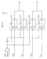
FIG. 4 is a schematic circuit diagram showing the selection unit 300.
As shown, the selection unit 300 includes a NAND gate ND1, an inverter I1, a first to a fourth transferring gates 310 to 340.
The NAND gate ND1 receives an extended mode register set selection signal EMRS_sel and a temperature sensor enable signal TS_en for performing a logic NAND operation to the extended mode register set selection signal EMRS_sel and the temperature sensor enable signal TS_en.
The inverter I1 inverts an output signal from the NAND gate ND1 and outputs the inverted signal to the second and the fourth transferring gates 320 and 340.
If the address A7 is 0, the first and the third transferring gates 310 and 330 transfer a first-bit TCSR code signal TCSR0 and a second-bit TCSR code signal TCSR1 of the TCSR code to the self refresh period signal generating unit 400.
On the other hand, if the address A7 is 1, the second and the fourth transferring gates 320 and 340 transfer a first-bit temperature sensor signal TS0 and a second-bit temperature sensor signal TS1 of the internal temperature sensor 200 to the self refresh period signal generating unit 400.
Meanwhile, the extended mode register set selection signal EMRS_sel is one of the bank address signals BA1 and BA0 which is in a logic high level. The temperature sensor enable signal TS_en is an inverted signal of the address A7.
Table. 3 shows a plurality of control codes included in the EMRS 100 in accordance with another embodiment of the present invention.
TABLE 3
Figure US07359270-20080415-C00005
Figure US07359270-20080415-C00006
As shown, the selection unit 300 uses the internal temperature sensor 200 for controlling the self refresh period signal generating unit 400 when both of addresses A4 and A3 are in a logic low level.
On the other hand, when at least one of the addresses A4 and A3 is in a logic high level, the selection unit 300 uses the TCSR code included in the EMRS 100 for controlling the self refresh period signal generating unit 400.
Herein, a temperature range from about 45° C. to about 70° C. is set to a default value.
As described above, the semiconductor memory device includes both the EMRS 100 and the internal temperature sensor 200 and selects one of them to control the self refresh period signal generating unit 400.
Therefore, the semiconductor memory device in accordance with the present invention can provide two control methods for controlling a self refresh period. One of the two control methods satisfies a Joint Electron Device Engineering Council (JEDEC) specification, and the other does not satisfy the JEDEC specification but a power consumption of a system where the semiconductor memory device is included can be reduced by using the other method. As a result, a user of the semiconductor memory device can select one of the two control methods depending on a system which the user uses or manufactures; and, a semiconductor memory device manufacturer can satisfy requirement of the user without manufacturing two different kinds of semiconductor memory devices having different control methods of the self refresh period.
In addition, the semiconductor memory device above described can be modified so that output signals from the EMRS 100 and the internal temperature are directly inputted to the self refresh period signal generating unit 400 and the self refresh period signal generating unit 400 selects one of them by modifying the self refresh period signal generating unit 400.
The present application contains subject matter related to Korean patent application No. 2003-76821, filed in the Korean Patent Office on Oct. 31, 2003, the entire contents of which being incorporated herein by reference.
While the present invention has been described with respect to the particular embodiments, it will be apparent to those skilled in the art that various changes and modifications may be made without departing from the spirit and scope of the invention as defined in the following claims.

Claims (7)

1. A self refresh period signal generating device comprising:
an extended mode register set for storing a first temperature code included in a set of control codes for the extended mode register set, wherein the first temperature code corresponds to temperature measured by an external temperature sensor and the set of control codes for the extended mode register set further includes a selection control code for determining which of the internal temperature sensor and the external temperature sensor is used;
an internal temperature sensor for measuring temperature wherein the internal temperature sensor is turned on or turned off in response to the selection control code;
a selection means for selecting one of the first temperature code included in the set of control codes for the extended mode register set and a second temperature code which corresponds to temperature measured by the internal temperature sensor in response to the selection control code; and
a self refresh period signal generating means for generating a temperature compensated self refresh period signal in response to an output signal from the selection means.
2. The self refresh period signal generating device as recited in claim 1, wherein the temperature code included in the set of control codes for the extended mode register set is a 2-bit code which corresponds to two bits of an address signal.
3. The self refresh period signal generating device as recited in claim 1, wherein the selection control code included in the set of control codes for the extended mode register set is a 1-bit code which corresponds to one bit of an address signal.
4. The self refresh period signal generating device as recited in claim 3, wherein the selection means includes:
a NAND gate for receiving the selection control code and a bank address; and
a plurality of transferring gates for outputting one of the first temperature code and the second temperature code depending on an output signal from the NAND gate.
5. The self refresh period signal generating device as recited in claim 1, wherein the first temperature code included in the set of control codes for the extended mode register set is a 2-bit code which corresponds to two bits of an address signal and the selection control code is one of four combinations of the 2-bit code.
6. The self refresh period signal generating device as recited in claim 5, wherein the selection means includes:
a NAND gate for receiving the selection control code and a bank address; and
a plurality of transferring gates for outputting one of the first temperature code and the second temperature code depending on an output signal from the NAND gate.
7. The self refresh period signal generating device as recited in claim 1, wherein the selection means includes:
a NAND gate for receiving the selection control code and a bank address; and
a plurality of transferring gates for outputting one of the first temperature code and the second temperature code depending on an output signal from the NAND gate.
US10/875,613 2003-10-31 2004-06-25 Self refresh period signal generation device Expired - Fee Related US7359270B2 (en)

Applications Claiming Priority (2)

Application Number Priority Date Filing Date Title
KR2003-76821 2003-10-31
KR1020030076821A KR100550634B1 (en) 2003-10-31 2003-10-31 Cell refresh cycle generator

Publications (2)

Publication Number Publication Date
US20060203589A1 US20060203589A1 (en) 2006-09-14
US7359270B2 true US7359270B2 (en) 2008-04-15

Family

ID=36970701

Family Applications (1)

Application Number Title Priority Date Filing Date
US10/875,613 Expired - Fee Related US7359270B2 (en) 2003-10-31 2004-06-25 Self refresh period signal generation device

Country Status (2)

Country Link
US (1) US7359270B2 (en)
KR (1) KR100550634B1 (en)

Cited By (3)

* Cited by examiner, † Cited by third party
Publication number Priority date Publication date Assignee Title
US20090154279A1 (en) * 2007-12-14 2009-06-18 Hynix Semiconductor, Inc. Refresh period signal generator with digital temperature information generation function
US20090238015A1 (en) * 2008-03-18 2009-09-24 Hynix Semiconductor Inc. Appartus and method for controlling refresh with current dispersion effect in semiconductor device
US10446217B2 (en) 2017-09-28 2019-10-15 Samsung Electronics Co., Ltd. Memory device and control method thereof

Families Citing this family (8)

* Cited by examiner, † Cited by third party
Publication number Priority date Publication date Assignee Title
JP4669258B2 (en) * 2004-10-13 2011-04-13 株式会社アドバンテスト Timing generator and test apparatus
KR100655076B1 (en) * 2005-01-20 2006-12-08 삼성전자주식회사 Internal temperature data output method of semiconductor memory device and corresponding internal temperature data output circuit
KR100832029B1 (en) * 2006-09-28 2008-05-26 주식회사 하이닉스반도체 Temperature information output device and semiconductor device having same
KR100904739B1 (en) 2007-12-28 2009-06-26 주식회사 하이닉스반도체 Temperature code transmission circuit and semiconductor memory device using same
US8180500B2 (en) * 2009-07-29 2012-05-15 Nanya Technology Corp. Temperature sensing system and related temperature sensing method
US8468295B2 (en) * 2009-12-02 2013-06-18 Dell Products L.P. System and method for reducing power consumption of memory
US9355704B2 (en) * 2012-12-28 2016-05-31 Mediatek Inc. Refresh method for switching between different refresh types based on at least one parameter of volatile memory and related memory controller
JP5867464B2 (en) * 2013-08-06 2016-02-24 コニカミノルタ株式会社 Information processing apparatus, refresh control program, and refresh control method

Citations (8)

* Cited by examiner, † Cited by third party
Publication number Priority date Publication date Assignee Title
US4639895A (en) * 1982-05-28 1987-01-27 Tokyo Shibaura Denki Kabushiki Kaisha Semiconductor memory device
US6256253B1 (en) * 2000-02-18 2001-07-03 Infineon Technologies North America Corp. Memory device with support for unaligned access
US20020191467A1 (en) * 2001-06-15 2002-12-19 Mitsubishi Denki Kabushiki Kaisha Semiconductor memory device
US20030056057A1 (en) * 2001-09-19 2003-03-20 Lawrence Richard H. System and method for power reduction of memory
US6768693B2 (en) * 2002-02-15 2004-07-27 Infineon Technologies Ag Integrated dynamic memory with control circuit for controlling a refresh mode of memory cells, and method for driving the memory
US20050105367A1 (en) * 2003-11-19 2005-05-19 Kim Jung P. Internal voltage generator with temperature control
US7009904B2 (en) * 2003-11-19 2006-03-07 Infineon Technologies Ag Back-bias voltage generator with temperature control
US7038968B2 (en) * 2004-04-13 2006-05-02 Hynix Semiconductor Inc. Self-refresh control circuit

Patent Citations (8)

* Cited by examiner, † Cited by third party
Publication number Priority date Publication date Assignee Title
US4639895A (en) * 1982-05-28 1987-01-27 Tokyo Shibaura Denki Kabushiki Kaisha Semiconductor memory device
US6256253B1 (en) * 2000-02-18 2001-07-03 Infineon Technologies North America Corp. Memory device with support for unaligned access
US20020191467A1 (en) * 2001-06-15 2002-12-19 Mitsubishi Denki Kabushiki Kaisha Semiconductor memory device
US20030056057A1 (en) * 2001-09-19 2003-03-20 Lawrence Richard H. System and method for power reduction of memory
US6768693B2 (en) * 2002-02-15 2004-07-27 Infineon Technologies Ag Integrated dynamic memory with control circuit for controlling a refresh mode of memory cells, and method for driving the memory
US20050105367A1 (en) * 2003-11-19 2005-05-19 Kim Jung P. Internal voltage generator with temperature control
US7009904B2 (en) * 2003-11-19 2006-03-07 Infineon Technologies Ag Back-bias voltage generator with temperature control
US7038968B2 (en) * 2004-04-13 2006-05-02 Hynix Semiconductor Inc. Self-refresh control circuit

Cited By (5)

* Cited by examiner, † Cited by third party
Publication number Priority date Publication date Assignee Title
US20090154279A1 (en) * 2007-12-14 2009-06-18 Hynix Semiconductor, Inc. Refresh period signal generator with digital temperature information generation function
US7859931B2 (en) 2007-12-14 2010-12-28 Hynix Semiconductor Inc. Refresh period signal generator with digital temperature information generation function
US20090238015A1 (en) * 2008-03-18 2009-09-24 Hynix Semiconductor Inc. Appartus and method for controlling refresh with current dispersion effect in semiconductor device
US7881140B2 (en) 2008-03-18 2011-02-01 Hynix Semiconductor Inc. Apparatus and method for controlling refresh with current dispersion effect in semiconductor device
US10446217B2 (en) 2017-09-28 2019-10-15 Samsung Electronics Co., Ltd. Memory device and control method thereof

Also Published As

Publication number Publication date
KR20050041600A (en) 2005-05-04
KR100550634B1 (en) 2006-02-10
US20060203589A1 (en) 2006-09-14

Similar Documents

Publication Publication Date Title
US6883061B2 (en) Electronic system and refresh method
US7710809B2 (en) Self refresh operation of semiconductor memory device
US7206244B2 (en) Temperature based DRAM refresh
US7359270B2 (en) Self refresh period signal generation device
US20080285370A1 (en) Semiconductor memory and system
US7317648B2 (en) Memory logic for controlling refresh operations
CN106782633B (en) Dynamic random access memory, method for storing data and reading and refreshing
US7180806B2 (en) Memory device, refresh control circuit to be used for the memory device, and refresh method
US6768693B2 (en) Integrated dynamic memory with control circuit for controlling a refresh mode of memory cells, and method for driving the memory
US7088635B2 (en) Bank based self refresh control apparatus in semiconductor memory device and its method
KR102403340B1 (en) Refresh control device
US7755966B2 (en) Memory device performing a partial refresh operation based on accessed and/or refreshed memory blocks and method thereof
KR100919558B1 (en) Semiconductor memory device using ferroelectric device and method for refresh thereof
US7269085B2 (en) Non volatile semiconductor memory device having a multi-bit cell array
US7167407B2 (en) Dynamic semiconductor memory device and power saving mode of operation method of the same
US20060171241A1 (en) Semiconductor memory device capable of selectively refreshing word lines
KR100506057B1 (en) Semiconductor memory device for performing partial array self refresh
US6414900B1 (en) Memory device and method for handling out of range addresses
US20140233332A1 (en) Semiconductor memory system
US20230221871A1 (en) Memory device and operating method thereof
JP4486836B2 (en) Nonvolatile ferroelectric memory cell array block and nonvolatile ferroelectric memory device using the memory cell array block
KR100477824B1 (en) Semiconductor memory device
US20080080284A1 (en) Method and apparatus for refreshing memory cells of a memory
US20080276053A1 (en) Portable Device and Method for Controlling Deep Power Down Mode of Shared Memory

Legal Events

Date Code Title Description
AS Assignment

Owner name: HYNIX SEMICONDUCTOR INC., KOREA, REPUBLIC OF

Free format text: ASSIGNMENT OF ASSIGNORS INTEREST;ASSIGNOR:LEE, JAE-YOUL;REEL/FRAME:016104/0924

Effective date: 20041215

FEPP Fee payment procedure

Free format text: PAYER NUMBER DE-ASSIGNED (ORIGINAL EVENT CODE: RMPN); ENTITY STATUS OF PATENT OWNER: LARGE ENTITY

Free format text: PAYOR NUMBER ASSIGNED (ORIGINAL EVENT CODE: ASPN); ENTITY STATUS OF PATENT OWNER: LARGE ENTITY

FEPP Fee payment procedure

Free format text: PAYER NUMBER DE-ASSIGNED (ORIGINAL EVENT CODE: RMPN); ENTITY STATUS OF PATENT OWNER: LARGE ENTITY

Free format text: PAYOR NUMBER ASSIGNED (ORIGINAL EVENT CODE: ASPN); ENTITY STATUS OF PATENT OWNER: LARGE ENTITY

FPAY Fee payment

Year of fee payment: 4

REMI Maintenance fee reminder mailed
LAPS Lapse for failure to pay maintenance fees
STCH Information on status: patent discontinuation

Free format text: PATENT EXPIRED DUE TO NONPAYMENT OF MAINTENANCE FEES UNDER 37 CFR 1.362

STCH Information on status: patent discontinuation

Free format text: PATENT EXPIRED DUE TO NONPAYMENT OF MAINTENANCE FEES UNDER 37 CFR 1.362

FP Lapsed due to failure to pay maintenance fee

Effective date: 20160415