US7339833B2 - Non-volatile semiconductor memory device - Google Patents
Non-volatile semiconductor memory device Download PDFInfo
- Publication number
- US7339833B2 US7339833B2 US11/481,782 US48178206A US7339833B2 US 7339833 B2 US7339833 B2 US 7339833B2 US 48178206 A US48178206 A US 48178206A US 7339833 B2 US7339833 B2 US 7339833B2
- Authority
- US
- United States
- Prior art keywords
- voltage
- write
- capacitance
- data
- writing
- Prior art date
- Legal status (The legal status is an assumption and is not a legal conclusion. Google has not performed a legal analysis and makes no representation as to the accuracy of the status listed.)
- Expired - Fee Related
Links
Images


Classifications
-
- G—PHYSICS
- G11—INFORMATION STORAGE
- G11C—STATIC STORES
- G11C11/00—Digital stores characterised by the use of particular electric or magnetic storage elements; Storage elements therefor
- G11C11/56—Digital stores characterised by the use of particular electric or magnetic storage elements; Storage elements therefor using storage elements with more than two stable states represented by steps, e.g. of voltage, current, phase, frequency
- G11C11/5621—Digital stores characterised by the use of particular electric or magnetic storage elements; Storage elements therefor using storage elements with more than two stable states represented by steps, e.g. of voltage, current, phase, frequency using charge storage in a floating gate
- G11C11/5628—Programming or writing circuits; Data input circuits
-
- G—PHYSICS
- G11—INFORMATION STORAGE
- G11C—STATIC STORES
- G11C11/00—Digital stores characterised by the use of particular electric or magnetic storage elements; Storage elements therefor
- G11C11/56—Digital stores characterised by the use of particular electric or magnetic storage elements; Storage elements therefor using storage elements with more than two stable states represented by steps, e.g. of voltage, current, phase, frequency
- G11C11/5621—Digital stores characterised by the use of particular electric or magnetic storage elements; Storage elements therefor using storage elements with more than two stable states represented by steps, e.g. of voltage, current, phase, frequency using charge storage in a floating gate
- G11C11/5642—Sensing or reading circuits; Data output circuits
-
- G—PHYSICS
- G11—INFORMATION STORAGE
- G11C—STATIC STORES
- G11C16/00—Erasable programmable read-only memories
- G11C16/02—Erasable programmable read-only memories electrically programmable
- G11C16/06—Auxiliary circuits, e.g. for writing into memory
- G11C16/10—Programming or data input circuits
-
- G—PHYSICS
- G11—INFORMATION STORAGE
- G11C—STATIC STORES
- G11C16/00—Erasable programmable read-only memories
- G11C16/02—Erasable programmable read-only memories electrically programmable
- G11C16/06—Auxiliary circuits, e.g. for writing into memory
- G11C16/34—Determination of programming status, e.g. threshold voltage, overprogramming or underprogramming, retention
- G11C16/3436—Arrangements for verifying correct programming or erasure
- G11C16/3454—Arrangements for verifying correct programming or for detecting overprogrammed cells
- G11C16/3459—Circuits or methods to verify correct programming of nonvolatile memory cells
-
- G—PHYSICS
- G11—INFORMATION STORAGE
- G11C—STATIC STORES
- G11C16/00—Erasable programmable read-only memories
- G11C16/02—Erasable programmable read-only memories electrically programmable
- G11C16/04—Erasable programmable read-only memories electrically programmable using variable threshold transistors, e.g. FAMOS
- G11C16/0408—Erasable programmable read-only memories electrically programmable using variable threshold transistors, e.g. FAMOS comprising cells containing floating gate transistors
- G11C16/0441—Erasable programmable read-only memories electrically programmable using variable threshold transistors, e.g. FAMOS comprising cells containing floating gate transistors comprising cells containing multiple floating gate devices, e.g. separate read-and-write FAMOS transistors with connected floating gates
- G11C16/0458—Erasable programmable read-only memories electrically programmable using variable threshold transistors, e.g. FAMOS comprising cells containing floating gate transistors comprising cells containing multiple floating gate devices, e.g. separate read-and-write FAMOS transistors with connected floating gates comprising two or more independent floating gates which store independent data
-
- G—PHYSICS
- G11—INFORMATION STORAGE
- G11C—STATIC STORES
- G11C16/00—Erasable programmable read-only memories
- G11C16/02—Erasable programmable read-only memories electrically programmable
- G11C16/04—Erasable programmable read-only memories electrically programmable using variable threshold transistors, e.g. FAMOS
- G11C16/0491—Virtual ground arrays
Definitions
- the present invention relates to a non-volatile semiconductor memory device and, more specifically, to a configuration of a portion related to data writing of a non-volatile semiconductor memory device performing a writing operation by introducing charges to a charge storage layer such as a floating gate. More specifically, the present invention relates to a configuration for highly precise control of threshold voltage distribution of a memory cell when multi-valued data is written.
- a non-volatile semiconductor memory device stores data utilizing the fact that threshold voltage of a memory cell transistor changes dependent on the amount of charges accumulated in the charge storage layer such as a floating gate. Dependent on the threshold voltage of the memory cell transistor, different amount of current flows when the memory cell is selected. By detecting the current flowing through the memory cell, data is read.
- charges are injected in accordance with information to be stored, in the charge storage layer of the memory cell transistor.
- a channel is formed at a surface of a semiconductor substrate region below the memory cell transistor, hot electrons are generated by accelerating current flowing through the channel, and the hot electrons are introduced into the charge storage layer such as the floating gate.
- the threshold voltage of memory cell transistor becomes higher (when the memory cell transistor is formed of an N-channel transistor). Therefore, distribution of threshold voltages that differ in multi-steps allows storage of different data using different threshold voltages, and hence, it becomes possible to store multi-valued data in one memory cell transistor.
- a non-volatile semiconductor memory device storing such multi-valued data is disclosed in Reference 1 (pamphlet of WO 2002/073623) and Reference 2 (Japanese Patent Laying-Open No. 11-330432).
- an MOS transistor is connected in series with a memory cell transistor.
- the MOS transistor functions as an assist gate or a select gate that is rendered conductive in accordance with a word line potential.
- An assist gate forms a channel at a surface of a semiconductor region of the underlying layer in accordance with an applied voltage, and functions as a diffusion source/drain line in data reading.
- the assist gate is set to a conductive state with relatively high resistance, and electrically couples adjacent memory cell transistors.
- a current is caused to flow from a drain region of one of the adjacent memory cell transistors to a source region of the other memory cell transistor.
- a high electric field generates in the channel region below the assist gate, and the high electric field produces channel hot electrons.
- An electric field in a vertical direction generated by a high voltage applied to a control gate (word line) of the memory cell transistor attracts the hot electrons toward the control gate, so that electrons are introduced to the floating gate.
- a select transistor connects an adjacent memory cell transistor to a bit line (data line) in accordance with the word line potential, to form a path of current flow for the memory cell transistor.
- data writing a current is supplied through the select transistor to a memory cell transistor, and hot electrons are generated by a high electric field at the drain, so that the electrons are introduced into the floating gate.
- a prescribed capacitance is connected to a drain bit line, and a write current is formed using charges accumulated in the capacitance.
- magnitude of a write current supplied to a memory cell is adjusted in accordance with the value of write data. This is to prevent a problem caused by a rush current in the initial stage of writing with the drain voltage kept constant, that is, to prevent the problem that excessive current flows to the memory cell and deteriorates memory cell characteristics.
- the amount of electrons to be injected is determined using parasitic capacitance of a metal bit line and a bit line of a diffusion layer as a capacitance for storing charges at the time of writing. Therefore, in the structure disclosed in Reference 1, the amount of electrons to be injected to a selected memory cell is determined by the amount of charges accumulated in the capacitance. Accordingly, the amount of change in the threshold voltage of the selected memory cell per one writing (injection) is constant. Typically, for writing multi-valued data, the threshold voltage is increased stepwise, and the data is written accordingly.
- Data “01” corresponds to a written (programmed) state with the highest threshold voltage and data “10” corresponds to a written (programmed) state with the lowest threshold voltage.
- the state storing data “11” corresponds to an erased state.
- the threshold voltage of memory cell transistor is adjusted in accordance with the stored data, with the erased state being the starting state.
- Reference 2 changes the amount of write current in accordance with the value of each write data, when multi-valued data is written.
- An arrangement utilizing a series-connection including a capacitor, a resistance and a diode is shown, as an example, for changing magnitude of a supplied write current in accordance with the write data.
- the capacitor By using the capacitor, the amount of charges to be supplied is adjusted and the amount of write current is adjusted accordingly.
- Reference 2 is directed to a cell structure of a memory cell transistor by itself, where an MOS transistor such as the assist gate is not connected in series with the memory cell transistor.
- MOS transistor such as the assist gate
- An object of the present invention is to provide a non-volatile semiconductor memory device allowing writing of multi-valued data accurately at high speed.
- the present invention provides a non-volatile semiconductor memory device, including: a plurality of non-volatile memory cells each for storing data of at least three values and each causing current flow of different amount in accordance with stored data; a plurality of first signal lines arranged corresponding to each column of the memory cells; a plurality of second signal lines arranged corresponding to each column of the memory cells; a capacitance control circuit changing a capacitance value of at least one of the first and second signal lines in accordance with a value of write data, when data is written to a memory cell; and a write control circuit supplying charges accumulated in one of the first and second signal lines as a write current to the selected memory cell.
- the other of the first and second signal lines receives the write current applied through the selected memory cell.
- the capacitance of a signal line supplying the write current is changed in accordance with the value of write data. Consequently, it becomes possible to supply charges of the amount corresponding to the write data, to the signal line supplying the write current. Therefore, variation in the threshold voltage can be suppressed to be comparable to the variation of charge injection efficiency, and the width of threshold voltage distribution can be made narrower.
- This achieves highly precise writing, and in writing multi-valued data the number of verifying operations for adjusting the width of threshold value distribution is reduced and hence the time for writing is reduced. Further, as the amount of supplied charges is adjusted in accordance with the value of write data, the amount of change in threshold voltage can be set in accordance with the write data. As a result, the number of times of data writing (injection) for writing data at a state of high threshold voltage is not much increased and, accordingly, the time necessary for data writing can be made shorter.
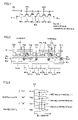
- FIG. 1 shows an exemplary arrangement of memory cells in a semiconductor memory device in accordance with the present invention.
- FIG. 2 shows voltages applied at the time of data writing to a series of memory cells shown in FIG. 1 .
- FIG. 3 illustrates correspondence between data stored in memory cells and threshold voltages.
- FIG. 4 schematically shows a configuration of a data writing unit in accordance with Embodiment 1 of the present invention.
- FIG. 5 is a diagram of waveforms representing an operation in data writing by the configuration shown in FIG. 4 .
- FIG. 6 schematically shows another sequence at the time of data writing by the configuration shown in FIG. 4 .
- FIG. 7 is a flow chart representing an operation in data writing of the semiconductor memory device in accordance with Embodiment 1 of the present invention.
- FIG. 8 schematically shows a configuration of a main portion of a non-volatile semiconductor memory device in accordance with Embodiment 2 of the present invention.
- FIG. 9 schematically shows another configuration of the main portion of the non-volatile semiconductor memory device in accordance with Embodiment 2 of the present invention.
- FIG. 10 schematically shows an overall configuration of a non-volatile semiconductor memory device in accordance with Embodiment 3 of the present invention.
- FIG. 11 shows an exemplary configuration of the memory array shown in FIG. 10 .
- FIG. 12 schematically shows a configuration of a charge capacitance control circuit shown in FIG. 10 .
- FIG. 13 schematically shows connection to divided global bit lines when the charge capacitance control circuit of FIG. 12 is used.
- FIG. 14 schematically shows a configuration of a sense/latch circuit of FIG. 10 .
- FIG. 15 schematically shows operational voltages in data writing and connection to memory cells, of the sense/latch circuit shown in FIG. 14 .
- FIG. 16 schematically shows capacitance distribution in data writing in accordance with Embodiment 3 of the present invention.
- FIG. 17 shows correspondence between the charge capacitance control circuit shown in FIG. 10 and switching elements.
- FIG. 18 schematically shows the charge capacitance control circuit shown in FIG. 10 and drain side and source side capacitance elements.
- FIG. 19 represents a first method of writing in data writing of a non-volatile semiconductor memory device in accordance with Embodiment 4 of the present invention.
- FIG. 20 shows connection of capacitance elements for a second method of writing in accordance with Embodiment 4 of the present invention.
- FIG. 21 is a diagram of waveforms in data writing by the configuration shown in FIG. 20 .
- FIG. 22 represents values of switching elements for a third method of writing in accordance with Embodiment 4 of the present invention.
- FIG. 23 is a diagram of waveforms in data writing with the configuration shown in FIG. 22 .
- FIG. 24 schematically shows a manner of connection of capacitance elements for a fourth method of writing in accordance with Embodiment 4 of the present invention.
- FIG. 25 schematically shows a manner of connection of capacitance elements at the time of data writing by a fifth method of writing in accordance with Embodiment 4 of the present invention.
- FIG. 26 schematically shows a manner of connection of capacitance elements in data writing by a seventh method of writing in accordance with Embodiment 4 of the present invention.
- FIG. 27 schematically shows a manner of connection of capacitance elements in data writing by an eighth method of writing in accordance with Embodiment 4 of the present invention.
- FIG. 28 schematically shows a manner of connection of capacitance elements at the time of data writing by a ninth method of writing in accordance with Embodiment 4 of the present invention.
- FIG. 29 is a waveform diagram representing an operation in data writing by the configuration shown in FIG. 28 .
- FIG. 30 schematically shows a manner of connection of capacitance elements in data writing by a tenth method of writing in accordance with Embodiment 4 of the present invention.
- FIG. 31 is a waveform diagram representing an operation in data writing by the configuration shown in FIG. 30 .
- FIG. 32 schematically shows a manner of connection of capacitance elements in data writing by an eleventh method of writing in accordance with Embodiment 4 of the present invention.
- FIG. 33 is a diagram of waveforms representing a writing operation by the configuration shown in FIG. 32 .
- FIG. 34 schematically shows a manner of connection of capacitance elements for a twelfth method of writing in accordance with Embodiment 4 of the present invention.
- FIG. 35 schematically shows a manner of connection of drain side capacitance elements in data writing of a non-volatile semiconductor memory device in accordance with Embodiment 5 of the present invention.
- FIG. 36 schematically shows a manner of connection of capacitance elements in injection for data writing in accordance with Embodiment 5 of the present invention.
- FIG. 37 schematically shows a manner of connection of capacitance elements at the time of re-injection in accordance with Embodiment 5 of the present invention.
- FIG. 38 is a diagram of waveforms representing the operations of configurations shown in FIGS. 35 to 37 .
- FIG. 39 shows an exemplary configuration of the capacitance control unit in accordance with Embodiment 5 of the present invention.
- FIG. 40 schematically shows a manner of connection of capacitance elements in re-charging a write voltage in accordance with Embodiment 5 of the present invention.
- FIG. 41 is a diagram of signal waveforms representing an operation in data writing by the configuration shown in FIG. 40 .
- FIG. 42 schematically shows a manner of connection of capacitance elements in when a write inhibiting voltage is transmitted, in accordance with Embodiment 6 of the present invention.
- FIG. 43 schematically shows a manner of connection of capacitance elements in transmitting a write inhibiting voltage, in accordance with Embodiment 6 of the present invention.
- FIG. 44 schematically shows a manner of connection of capacitance elements at the time of injecting electrons in accordance with Embodiment 6 of the present invention.
- FIG. 45 schematically shows a manner of connection of capacitance elements in transmitting a write inhibiting voltage, in accordance with Embodiment 5 of the present invention.
- FIG. 46 schematically shows a manner of connection of capacitance elements in transmitting a write inhibiting voltage, in accordance with Embodiment 6 of the present invention.
- FIG. 47 schematically shows another example of the manner of connection of capacitance elements at the time when a write inhibiting voltage is re-charged, in accordance with Embodiment 6 of the present invention.
- FIG. 48 is a flowchart representing an operation in data writing of a non-volatile semiconductor memory device in accordance with Embodiment 7 of the present invention.
- FIG. 49 is a flowchart representing another operation sequence in data writing of the non-volatile semiconductor memory device in accordance with Embodiment 7 of the present invention.
- FIG. 50 is a schematic illustration showing the amount of cycle-by-cycle change in threshold voltage in data writing shown in FIGS. 48 and 49 .
- FIG. 51 schematically shows a sequence of change in a word line programming voltage at the time of writing of a non-volatile semiconductor memory device in accordance with the present invention.
- FIG. 52 schematically shows an exemplary configuration of a portion generating the word line programming voltage shown in FIG. 51 .
- FIG. 53 shows an example of a sequence of change in a drain write voltage in accordance with Embodiment 8 of the present invention.
- FIG. 54 shows another example of a sequence of change in a drain write voltage in accordance with Embodiment 8 of the present invention.
- FIG. 55 schematically shows an exemplary configuration of a portion generating a drain write voltage shown in FIGS. 53 and 54 .
- FIG. 1 schematically shows an arrangement of memory cells of a non-volatile semiconductor memory device to which the present invention is applied.
- memory cells MCa to MCd are connected to a word line WL.
- an assist gate AGTa is arranged, and between memory cells MCc and MCd, an assist gate AGTb is arranged.
- assist gate selecting signals AG 0 and AG 1 are applied, respectively.
- Memory cells MCa to MCc are formed of stacked gate type transistors having a floating gate, and a node opposite to a node connected to the assist gate is connected to a diffusion line DL (DLa to DLc) formed of an impurity diffusion layer of low resistance.
- Assist gates AGTa and AGTb continuously extend in the column direction, in the same direction as diffusion lines DLa to DLc, and form inverted layers at the surface of substrate regions immediately below the gates, in accordance with assist gate selecting signals AG 0 and AG 1 , respectively.
- These assist gates AGTa and AGTb do not have source/drain regions and they simply form inversion layers at the surface of substrate region immediately therebelow, in accordance with assist gate selecting signals AG 0 and AG 1 .
- assist gates AGTa and AGTb are represented by the same symbol as common MOS transistors, as they form inversion layers.
- Diffusion layers are further connected selectively to a metal interconnection line (global bit line) through a select gate.
- assist gate AGTa or AGTb is set to a selected state and forms an inversion layer therebelow, and the inversion layer serves as a source line.
- a selected memory cell has its corresponding diffusion line DL connected to the global bit line (metal interconnection line).
- assist gate selecting signal AG 0 attains to the selected state of H level and assist gate selecting signal AG 1 attains to the unselected state of L level. Therefore, an inversion layer is formed below assist gate AGTa, that is, a source line for memory cell MCa is formed. Diffusion line DLb is connected to the global bit line.
- a read current is supplied to diffusion line DLb, and a current corresponding to the stored data is caused to flow through the inversion layer of assist gate AGTa. By detecting the amount of current flowing through diffusion line DLb, the data stored in memory cell MCb is read.
- assist gate selecting signal AG 1 is in the unselected state and the inversion layer is not formed below assist gate AGTb, and in memory cell MCc, even when the word line WL is selected, a read current does not flow.
- diffusion line DLa is in a floating state or set to a ground voltage level, so that no current flows to memory cell MCa. Therefore, it is possible to cause a current to flow through diffusion line DLb in accordance with the data stored in memory cell MCb, and to correctly read the memory cell data.
- SSI Source Side Injection
- FIG. 2 shows a cross-sectional structure of the memory cell arrangement shown in FIG. 1 and voltages applied to various nodes at the time of data writing.
- FIG. 2 additionally shows memory cells MCe and MCf as well as an assist gate AGTc arranged between these memory cells MCe and MCf.
- Diffusion lines DLa, DLb and DLc are formed of impurity regions spaced from each other at a surface of a semiconductor substrate region (well region) WELL and each serve as a source/drain region of the memory cell transistor.
- Memory cells MCa to MCf respectively have one conduction node (source/drain node) formed by diffusion lines DLa, DLb and DLc arranged adjacent thereto.
- FIG. 2 also shows a diffusion line DLe provided for memory cell MCf.
- These memory cells MCa to MCf each include a floating gate FG, and have a control gate formed by a word line WL provided on floating gate FG.
- Assist gates AGTa, AGTb and AGTc are each formed of an assist gate line AGL, and assist gate line AGL is arranged between the floating gates of adjacent memory cells.
- assist gate line AGL is arranged between the floating gates of adjacent memory cells.
- an inversion layer IVL is formed at the surface of substrate region WELL.
- the term “assist gate AGT” will be used to refer to the assist gate line AGL and the inversion layer therebelow.
- a positive high voltage Vpp for writing is supplied to word line WL.
- a drain write voltage Vwd is supplied to diffusion line DLa, and diffusion line DLb is set to the ground voltage VSS.
- a gate write (programming) voltage Vpf of, for example, about 0.6V to 1.5V is applied to assist gate line AGL of assist gate AGTa.
- Assist gates AGTa and AGTc commonly receive assist gate selecting signal AG 0 shown in FIG. 1 and, therefore, the gate write voltage Vpg of the same voltage level is supplied to assist gate lines AGL of assist gates AGTa and AGTc, whereby inversion layers IVL are formed at the surfaces of the substrate regions below these gates.
- the selecting voltage is not applied to assist gate line AGL of assist gate AGTb and it is maintained at the ground voltage level, so that the inversion layer is not formed therebelow.
- a write inhibiting voltage Vihb is supplied to diffusion line DLc.
- word line write voltage Vpp is 15V
- assist gate write voltage Vpg is 0.6V to 1.5V
- drain write voltage Vwd is 4.5V
- write inhibiting voltage Vihb is 2V.
- FIG. 2 shows the flow of electron “ ⁇ e.”
- the voltage level of gate programming voltage Vpg is, for example, 1.5V, which is slightly higher than the threshold voltage of the assist gate, and the inversion layer IVL of assist gate AGTa has a relatively high resistance. Therefore, the current flowing from diffusion line DLa generates hot electrons because of a high electric field near the inversion layer IVL of assist gate AGTa, and the hot electrons are drawn in the direction along the word line and injected to the floating gate above (represented by the hatching), by an electric field in the vertical direction derived from the high voltage of word line WL.
- the threshold voltage of memory cell MCa becomes higher (assuming that the memory cell transistor is an N-channel type transistor).
- the writing operation of injecting electrons to the floating gate from the source side of memory cell MCa is referred to as the source side injection (SSI) writing.
- inversion layer IVL is formed at assist gate AGTe, and therefore, a current flows from diffusion line DLc to diffusion line DLd.
- write inhibiting voltage Vihb is supplied, and voltage difference between diffusion lines DLc and DLd is small. Therefore, electrons are not so much accelerated as to generate hot electrons, and hence, injection of electrons to the floating gate of memory cell MCe does not occur. Accordingly, data writing to memory cell MCe is inhibited.
- the threshold voltages of memory cells MCa to MCf are determined in accordance with the amounts of current injected to respective floating gates. Therefore, by charging the write voltage Vwd supplied to diffusion line DLa to capacitance element Cda and using the accumulated charges as the write current, the amount of electrons injected to the floating gate FG of memory cell MCa can be adjusted and, accordingly, the amount of change in the threshold voltage can be adjusted.
- FIG. 3 shows a relation between respective data values and the threshold voltages when 4-valued data is used as the multi-valued data.
- the ordinate represents threshold voltage Vth and the abscissa represents number of bits of the memory cells.
- a state storing data “11” corresponds to an erased state, and the central value of threshold voltage distribution is Vth 0 .
- States storing data “10”, “00” and “01” are written states (programmed states), and the central threshold voltages of the threshold voltage distributions are Vth 1 , Vth 2 and Vth 3 , respectively.
- the upper and lower limits of threshold value distributions corresponding to the 4-valued data respectively are determined beforehand and writing of data (injection of electrons) is performed such that the threshold voltage of the memory cell falls within the threshold voltage range between the upper and lower limits.
- the threshold voltage Vth is set to the lowest value. From this state, writing operations ( 1 ), ( 2 ) and ( 3 ) are executed to the memory cells as the objects of writing, in accordance with the write data, so that respective threshold voltages increase. Therefore in writing operation ( 1 ) of writing data “01”, the threshold voltage changes the most, the amount of change in the threshold voltage is second largest in writing operation ( 2 ) of writing “00”, and the amount of change in the threshold voltage is the smallest in writing operation ( 3 ) of writing “10”. The amount of change in the threshold voltage is determined by the amount of electrons injected to the floating gate.
- FIG. 4 schematically shows a configuration of a write capacitance control unit in accordance with Embodiment 1 of the present invention.
- connection of memory cells MC 0 and MC 1 at the time of data writing is shown as a representative.
- Memory cells MC 0 and MC 1 have their control gates connected to the word line WL.
- a source node DLS of memory cell MC 0 receives (through diffusion line) the ground voltage VSS.
- an assist gate AGT is arranged, and a control gate of assist gate AGT forms a part of an assist gate line AGL.
- Switching elements DSW 0 to DSWn ⁇ 1 are connected in series with a drain node DLB of memory cell MC 1 .
- Capacitance elements CD 0 to Cdn ⁇ 1 are arranged between nodes ND 0 to NDn ⁇ 1 corresponding to switching elements DSW 0 to DSWn ⁇ 1 and the ground node.
- Switching elements CSW 0 to CSWn ⁇ 1 for charging which are coupled to a write voltage supplying node CPS when in conductive state, are connected respectively to nodes ND 0 to NDn ⁇ 1.
- data is written to memory cell MC 0 , and a current flows from the drain node (diffusion line) DLD of memory cell MC 1 .
- the data written to memory cell MC 0 is multi-valued data and, in accordance with the value of write data, the number of capacitance elements C 0 to Cn ⁇ 1 to be connected to drain node DLD is adjusted by rendering conductive/non-conductive the switching elements DSW 0 to DSWn ⁇ 1 at the time of selection.
- the capacitance value of capacitance elements coupled to drain node DLD is adjusted and hence, the amount of accumulated charges is adjusted.
- the verifying operation for writing operations ( 1 ), ( 2 ) and ( 3 ) the number of rewriting cycles can be reduced and hence the time necessary for writing can be reduced. Further, as the width of threshold voltage distribution becomes narrower, it becomes possible to store multi-valued data with high precision.
- FIG. 5 is a diagram of signal waveforms representing an operation at the time of data writing by the circuit shown in FIG. 4 .
- FIG. 5 shows an example in which writing operation ( 1 ) of FIG. 3 is performed, utilizing charges accumulated in all capacitance elements Cd 0 to Cdn ⁇ 1.
- word line WL is driven to a selected state of a high voltage level for writing, and voltage level of node CPS for supplying write voltage is increased to a write voltage level.
- switching elements DSW 0 to DSWn ⁇ 1 are all selectively set to the conductive (ON) state.
- switching elements DSW 0 to DSWn ⁇ 1 are all rendered conductive.
- Switching elements DSW 0 to DSWn ⁇ 1 are successively and sequentially set to the conductive state after the word line WL has been driven to the selected state of writing high voltage level, in order to prevent the change in capacitance of drain node (diffusion line) DLD from affecting the selecting operation of word line WL. Further, switching elements DSW 0 to DSWn ⁇ 1 are successively and sequentially rendered conductive in order to prevent any change in voltage of an internal node caused by noise when the capacitance value changes as the capacitance elements are connected.
- switching elements CSW 0 to CSWn ⁇ 1 for charging are rendered conductive, and the drain write voltage is supplied from write voltage supplying node CPS to capacitance elements Cd 0 to Cdn ⁇ 1.
- switching elements DSW 0 to DSWn ⁇ 1 are all on, and the voltage level of drain node DLD increases in accordance with the charging operation.
- switching elements CSW 0 to CSWn ⁇ 1 for charging are all non-conductive, and write voltage supplying node CPS is isolated from corresponding nodes ND 0 to NDn ⁇ 1. Therefore, only the charges that have been accumulated in capacitance elements Cd 0 to Cdn ⁇ 1 are supplied to drain node DLD, and even when memory cell MC 1 has low threshold voltage at the start of writing, flow of a large current can be prevented.
- FIG. 6 is a diagram of waveforms representing writing operation ( 3 ) shown in FIG. 3 .
- the data writing operation of FIG. 6 differs from the writing operation of FIG. 5 in the following points. Specifically, in period P 1 of activating the write power supply for the word line, switching elements DSW 0 and DSW 1 are set to the conductive state, and remaining switching elements (DSW 2 (not shown) to DSWn ⁇ 1) are kept non-conductive. Thus, capacitance elements Cd 0 and Cd 1 are connected in series with drain node DLD.
- the time width of period P 2 necessary for charging can be made shorter than when all the capacitance elements Cd 0 to Cdn ⁇ 1 are to be charged. Therefore, in accordance with the number of capacitance elements used or with the value of write data, that is, in accordance with the amount of accumulated charges used for writing, the time width of period P 2 of accumulating drain charges is adjusted. Thus, the overall time necessary for writing all the data can be made shorter.
- period P 3 of injecting charges injection period, assist gate line AGL is driven to the selected state, and the inversion layer is formed at assist gate AGT shown in FIG. 4 .
- the amount of charges (electrons) injected to the floating gate of memory cell MC 1 is small, and therefore, period P 3 necessary for electron injection can be made short.
- Data writing injection of electrons to the floating gate automatically stops, when voltage difference between drain node DLD and source node DLS attains to a prescribed value or lower and generation of hot electrons stops.
- Time width of periods P 2 and P 3 may be adjusted in accordance with the value of write data. Further, the switching element or elements to be set to the conductive state among switching elements GSW 0 to GSWn 0 ⁇ 1 and CSW 0 to CSWn ⁇ 1 may be set in accordance with the value of write data.
- FIG. 7 is a flow chart representing an operation at the time of data writing according to Embodiment 1 of the present invention. In the following, the operation at the time of data writing according to Embodiment 1 of the present invention will be described with reference to FIG. 7 .
- a write command is applied from an outside of the memory, together with an address (step SP 1 ).
- data writing is designated, and the start address for writing data is designated.
- write data is applied (step SP 2 ).
- write data write data corresponding to the number of data for a unit of writing are transferred.
- write data are stored in an internal write data register.
- step SP 3 After all write data are transferred, a write execution command is applied, and an internal writing operation starts (step SP 3 ).
- step SP 4 the data that have been written and stored in data register (SRAM: Static Random Access Memory) in step SP 2 are transferred to a sense amplifier latch (SL) (step SP 4 ).
- writing of data “01” (writing operation ( 1 )) is executed, and therefore data “01” is transferred to sense amplifier latch SL arranged corresponding to each column of memory cells.
- write inhibition write inhibiting voltage
- a threshold value changing sequence WOF for actually writing data to the selected memory cell is executed.
- a write power supply is activated (step SPP 1 ).
- the write power supply includes internal voltage generating circuits respectively generating a word line write voltage, a drain write voltage applied to the drain node of a memory cell, a gate program voltage applied to the assist gate line in writing and the like.
- Each of the voltage generating circuits of the write power supply may be formed, for example, by a circuit utilizing a charge-pump operation of a capacitor.
- the write word line is driven to the selected state, and the write inhibiting voltage (Vihb) for inhibiting data writing is transmitted to memory cells that are not the object of writing, so that the voltage of the source node is set to either one of the ground voltage and the write inhibiting voltage (step SPP 2 ).
- charge accumulating capacitance for accumulating charges to be transmitted to the drain node is set (step SPP 3 ).
- the charge accumulating capacitance is set by selectively setting each of the drain switching elements (DSW 0 to DSWn ⁇ 1) to the conductive state in period P 1 shown in FIG. 6 .
- Charges from the drain write voltage generating unit included in the write power supply are accumulated in the drain side capacitance elements (Cd 0 , . . . ) and the parasitic capacitance of drain node.
- step SPP 5 When accumulation of drain charges is completed, data writing to the memory cell is performed (step SPP 5 ).
- step SPP 5 of charge injection the voltage of assist gate line is driven to the selected state to cause a memory cell current to flow, whereby electrons are injected to the floating gate of the selected memory cell.
- a write terminating process is performed, in which the voltage level of the write word line is lowered, and a write-verifying voltage is set for determining whether writing has been done successfully (step SPP 6 ).
- the written data is read, and whether the threshold voltage of the memory cell to which data “01” has been written satisfies the condition of threshold voltage distribution range for data “01” or not is determined (step SPP 8 ).
- step SPP 8 when it is determined that the threshold voltage of memory cell is out of the distribution range, the operation from step SPP 1 is repeated on the memory cell of which writing has been unsuccessful.
- writing is inhibited to the memory cell of which threshold voltage is determined to be normal (the write inhibiting voltage is set or latched data of the corresponding sense latch is set to the write-complete state).
- the threshold value changing sequence WOF for data “01” is completed.
- step SP 5 the threshold changing sequence WOF similar to that for writing data “01” is executed.
- step SPP 3 of setting charge accumulating capacitance the number of accumulating capacitances used is reduced, and in step SPP 4 of accumulating drain charges, the time period of charge accumulation is made shorter. Further, at step SPP 5 of charge injection, the time period of charge injection is made shorter.
- steps SPP 1 to SPP 3 correspond to the period P 1 of word line activation and power supply activation shown in FIGS.
- step SPP 4 of accumulating drain charges corresponds to period P 2 of accumulating drain charges.
- step SPP 5 of charge injection corresponds to P 3 .
- Step SPP 6 corresponds to the process period P 4 for the write termination process and the write-verify.
- step SP 6 After completion of threshold value changing sequence WOF for data “00”, writing of data “10” takes place (step SP 6 ).
- step SP 6 the data “10” that has been stored in the data register (SRAM) is transferred to the sense amplifier latch (SL).
- step SP 6 the threshold changing sequence WOF similar to that for writing data “01” and “00” is executed.
- the write power supply system is inactivated and the data writing ends (step SP 7 ).
- the capacitance for charge accumulation at the drain node connected to the memory cell may be implemented by using, for example, an MOS capacitor connected independently to each drain diffusion layer, or parasitic capacitance of diffusion line may be used. A configuration that implements variable capacitance for charge accumulation will be described in detail later.
- Memory cell structure is not limited to a so-called AG_AND flash memory using an assist gate, and the invention is similarly applicable to a memory cell structure having a selection transistor connected in series with the memory cell transistor.
- the charge accumulating layer for accumulating charges is not limited to the floating gate, and a charge trap insulating film, accumulating charges in a nitride film of an ONO (oxide-nitride-oxide) film, may be used as the charge accumulating layer.
- a charge trap insulating film accumulating charges in a nitride film of an ONO (oxide-nitride-oxide) film, may be used as the charge accumulating layer.
- Embodiment 1 of the present invention for a memory cell in which multi-valued data is to be stored, the amount of charge accumulation is adjusted in accordance with the value of the write data, a write current is generated by the accumulated charges and injected to the charge accumulating layer such as the floating gate of the memory cell. Therefore, the amount of electrons injected to the charge accumulating layer of the memory cell at one write cycle can accurately be adjusted and the width of threshold voltage distribution of the memory cell after data writing can be made narrower, so that highly precise writing becomes possible and the time necessary for writing can be reduced (as the number of times of verifying operations can be reduced).
- FIG. 8 schematically shows a configuration of a main portion of a non-volatile semiconductor memory device according to Embodiment 2 of the present invention.
- the configuration shown in FIG. 8 differs from that of FIG. 4 in the following point. Specifically, in the configuration shown in FIG. 8 , capacitance element Cs is connected also to the source node DLS of memory cell MC 0 . Except for this point, the configuration shown in FIG. 8 is the same as that of FIG. 4 . Therefore, corresponding portions are denoted by the same reference characters and detailed description thereof will not be repeated.
- Embodiment 2 of the present invention charges are distributed between capacitance Dc (combined capacitance of capacitances used among Cd 0 to Cdn ⁇ 1) of drain node DLD and capacitance Cs connected to the source node (diffusion line) DLS, so that a current is caused to flow between the source/drain of the memory cell and data is written in accordance with source side injection method.
- the manner of adjusting the capacitance of charge accumulation connected to drain node DLD is the same as that in Embodiment 1 above.
- the magnitude of a capacitance connected to drain node DLD is represented by Cd and the magnitude of a capacitance connected to source node DLS is represented by Cs. It is assumed that the capacitance Cs of source node DLS is initially in a discharged state.
- Vsd represents voltage of source node DLS and drain node DLD after charge distribution.
- the capacitance value Cs of source node DLS, capacitance value Cd of the drain node and the drain write voltage Vcps can be set to exact values, respectively. Therefore, the amount of charges Qd that move from the drain node DLD to the source node DLS can be set exactly and hence, the amount of electrons injected to the floating gate of the memory cell in one write cycle can be set exactly. Therefore, data writing with higher precision and limited distribution width of threshold voltage becomes possible.
- FIG. 9 schematically shows a configuration of a first modification of the non-volatile semiconductor memory device according to Embodiment 2.
- the configuration shown in FIG. 9 differs from that of non-volatile semiconductor memory device shown in FIG. 8 in the following point.
- a plurality of capacitance elements Cs 0 to Csm ⁇ 1 are provided as capacitance elements connected to source node DLS.
- switching elements SSW 0 to SSWm ⁇ 1 for adjusting source capacitance values are arranged and connected in series.
- the configuration of non-volatile semiconductor memory device shown in FIG. 9 is the same as that of non-volatile semiconductor memory device shown in FIG. 8 . Therefore, corresponding portions are denoted by the same reference characters and detailed description thereof will not be repeated.
- the capacitance value of capacitance elements connected to the source node DLS can be adjusted. Therefore, as compared with the configuration shown in FIG. 8 , the amount of charges transferred from the drain node DLD to the source node DLS can more delicately be adjusted. Specifically, from the equations above, it is understood that the amount of charges Qd that move from the node DLD on the drain side to the node DLS on the source side is in proportion to 1/((1/Cd)+(1/Cs)). Therefore, by adjusting the capacitance values of drain node capacitance Cd and source node capacitance Cs, the amount of charges that move can be adjusted.
- the node capacitance Cs on the source side When the node capacitance Cs on the source side is sufficiently larger than the capacitance of drain node Cd, the charges accumulated in node DLD on the drain side can be transferred, and when, on the other hand, the node capacitance Cs on the source side is smaller than the capacitance Cd on the side of the drain node, the amount of charges transferred form the drain node to the source node becomes smaller.
- the source capacitance corresponds to infinite value.
- the amount of charges to be transferred in one writing operation (operation of injecting electrons to the floating gate; one writing operation will be hereinafter referred to as an injection) can be adjusted with high precision, the amount of electrons to be injected can be adjusted, and the variation in threshold voltages can be reduced.
- Embodiment 2 of the present invention capacitances are connected to the source side and drain side of the memory cell, and a write current is generated by utilizing electron distribution among the capacitances. Therefore, more delicate adjustment in the amount of write charges becomes possible, variation in threshold voltages can be suppressed, and writing with high precision becomes possible.
- FIG. 10 schematically shows an overall configuration of a non-volatile semiconductor memory device according to Embodiment 3 of the present invention.
- the non-volatile semiconductor memory device shown in FIG. 10 implements the configurations of Embodiments 1 and 2 described above.
- the non-volatile semiconductor memory device includes memory array groups MG 0 to MG(M ⁇ 1) each including a plurality of (in the example of FIG. 10 , four) memory arrays.
- Memory array group MG 0 includes memory arrays MA 0 to MA 3
- memory array group MG(M ⁇ 1) includes memory arrays MA(N ⁇ 4) to MA(N ⁇ 1).
- memory cells are arranged in a matrix of rows and columns. A word line is provided corresponding to each row of memory cells, and a bit line is provided corresponding to each column of memory cells, to be shared by adjacent columns.
- a global bit line GBL provided common to the columns of memory cells in memory arrays MA 0 to MA(N ⁇ 1) is shown as a representative.
- the bit line of the memory array (or the assist gate line) is coupled to a corresponding global bit line through a select gate.
- word line decoders XD to XD(M ⁇ 1) are provided.
- Word line decoders XD 0 to XD(M ⁇ 1) when selected, drive the word line to the selected state in one of the memory arrays of the corresponding memory array group.
- charge capacitance control circuits CCC 0 to CCC(M ⁇ 1) are provided.
- charge capacitance control circuits CCC 0 to CCC(M ⁇ 1) By charge capacitance control circuits CCC 0 to CCC(M ⁇ 1), the capacitance values of charge accumulating capacitances of the drain node and the source node of selected memory cell are adjusted.
- the non-volatile semiconductor memory device further includes: an interface circuit 1 receiving external control signals /CE, /WE, /RE, ALE, CLE and R/B and outputting data I/O 0 to I/O 7 ; a control circuit 2 receiving a control signal from interface circuit 1 and generating a necessary control signal in accordance with the designated operation mode; a power supply circuit 3 generating an internal voltage under the control of control circuit 2 ; and a voltage switching circuit 4 switching voltage level and voltage polarity of the voltage generated by power supply circuit 3 .
- Power supply circuit 3 generates an internal voltage necessary for writing, reading and verifying.
- Voltage switching circuit 4 sets the internal voltage generated by power supply circuit 3 to the voltage level designated by control circuit 2 .
- voltage switching circuit 4 is shown generating a drain write voltage VWD, a word line write voltage VPP and a negative voltage VNN, as an example.
- the negative voltage VNN is used in an erasure mode.
- Voltages VPP and VNN are applied to word line decoders XD 0 to XD(M ⁇ 1), and in the write mode, the selected word line is set to the positive high voltage VPP and in the erasure mode, the selected word line is set to the negative voltage VNN.
- the drain write voltage VWD is supplied to a write voltage supplying node (CPS) of the charge capacitance control circuit, at the time of data writing.
- CPS write voltage supplying node
- Control signal /CE is a chip enable signal indicating that the non-volatile semiconductor memory device is selected and an operation related to a data access will be performed on the semiconductor memory device.
- Control signal /WE is a write enable signal, indicating that a data writing mode is designated.
- Control signal /RE is a read enable signal, indicating that data reading is designated.
- Control signal ALE is an address latch signal, providing an instruction for latching an applied address signal (generally applied through a data input/output terminal) to an address buffer included in interface circuit 1 and providing latch timing.
- Control signal CLE is a command latch enable signal, similarly designating a mode for taking an external command into a command buffer included in interface circuit 1 and providing a latch timing.
- Control signal R/B is a ready/busy signal indicating that it is ready for data writing, and that data writing and verifying operations are being performed inside and any external access cannot be accepted.
- Interface circuit 1 includes an input/output buffer transmitting/receiving data I/ 00 to I/ 07 , an address buffer latching an address signal, a command buffer latching a command, and an input/output control circuit for input/output control (determining direction of data transfer for writing and reading), and operation timings are given in accordance with the control signals described above.
- a data register 7 is provided for transferring internal data to/from interface circuit 1 through data bus 6 .
- Data register receives and latches data read from a memory cell of a selected row of a selected memory array, and latches write data to a selected memory cell in data writing.
- register circuits are arranged corresponding to columns of memory cell for transferring data to/from the corresponding column (global bit line).
- a sense/latch circuit 8 For executing write operations ( 1 ) to ( 3 ) shown in FIG. 3 at the time of data writing, a sense/latch circuit 8 taking and latching data from data register 7 is provided.
- Sense/latch circuit 8 includes a sense amplifier provided corresponding to each column of memory arrays MA 0 to MA(M ⁇ 1), and in data writing, receives and latches data transferred from data register 7 .
- data register 7 In data writing, data register 7 generates data for executing or inhibiting data writing for each column in accordance with stored data, and transfers the generated data to sense/latch circuit 8 .
- a write inhibiting voltage is generated for inhibiting writing in each of writing operations ( 1 ) to ( 3 ).
- the capacitance value of capacitances accumulating charges for writing is adjusted by charge capacitance control circuits CCC 0 to CCC(M ⁇ 1).
- the value of drain side capacitance or source side capacitance may be adjusted in each of the charge capacitance control circuits CCC 0 to CCC(M ⁇ 1).
- parasitic capacitances of diffusion lines (source diffusion line and drain diffusion line) and of the global bit line coupled to sense/latch circuit 8 are utilized, and by adjusting the length of these lines, the capacitance value is adjusted and the layout area of the memory mat (memory array arranging area) is reduced. Specific configurations of various portions will be described in the following.
- FIG. 11 schematically shows a configuration of memory arrays MA 0 to MA(M ⁇ 1) of FIG. 10 .
- Memory arrays MA 0 to MA(M ⁇ 1) each have the same configuration and, therefore, FIG. 11 shows memory array MA as a representative of these memory arrays MA 0 to MA(M ⁇ 1).
- memory array MA includes memory cells MC arranged in a matrix of rows and columns.
- Memory cells MC include four different kinds of memory cells, that is, MC 0 to MC 3 , which are connected in different manners at the time of data writing. At the time of data writing, data are written in parallel to memory cells of the same kind.
- assist gate AGT 1 is arranged between memory cells MC 0 and MC 1 , assist gate AGT 1 is arranged, and between memory cells MC 2 and MC 3 , assist gate GT 0 is arranged.
- Word line WL is arranged corresponding to each row of memory cells, and control gates of memory cells MC 0 to MC 3 are commonly connected to the corresponding word line WL (control gate of each memory cell form a part of the word line WL).
- FIG. 11 shows an example in which 256 word lines WL 0 to WL 255 are arranged as the word lines WL.
- Assist gates AGT 1 arranged aligned in the column direction share assist gate line AGL 1 , and when selected, form inversion layers INV 1 , at the surface of semiconductor substrate regions therebelow, continuously extending in the column direction.
- Assist gates AGT 0 share assist gate line AGL 0 and, when selected, form inversion layers INV 0 thereblow, continuously extending in the column direction.
- assist gates are shown as arranged independently and separately in each column in FIG. 11
- assist gates AGT 0 and AGT 1 shown to be arranged aligned in the column direction are each implemented by one MOS transistor formed by the inversion layer forming region extending continuously in the column direction and assist gate line AGL and having its channel width set in the column direction.
- inversion layers INV 0 and INV 1 form a pair and are coupled to source lines IS (IL 1 , IS 2 and IL 3 ).
- a diffusion layer DL 1 is provided commonly to one conduction node of each of memory cells MC 1 and MC 2 , which diffusion layer DL 1 extends continuously along the column direction to form the diffusion line.
- a diffusion layer DL 0 is commonly coupled to one conduction node of each of memory cells, and the diffusion layer DL 0 extends continuously along the column direction to form the diffusion line.
- FIG. 11 shows a state in which global bit lines GBLj ⁇ 2 to GBLj+4 are arranged.
- Global bit lines GBLj ⁇ 2 to GBLj+4 are commonly provided for memory arrays MA 0 to MA(N ⁇ 1) shown in FIG. 10 .
- Global bit line GBL is selectively used as a source side bit line or a drain side bit line, in accordance with the position (kind) of the selected memory cell.
- selection transistors SDT 00 , SDT 01 , SDT 02 and SDT 03 coupling a diffusion layer DL 0 to global bit lines GBLj ⁇ 2 GBLj, GBLj+2 and GBLj+4, respectively, in accordance with the diffusion line selecting signal (drain selecting signal) SD 0
- selection transistors SDT 10 , SDT 11 and SDT 12 coupling a diffusion layer DL 1 to global bit lines GBLj ⁇ 1, GBLj+1 and GBLj+3 arranged in the corresponding columns, respectively, in accordance with the diffusion line selecting signal SDT 1 .
- an assist gate selecting signal AG 0 is applied to the assist gate line AGL 0 , that is, to the corresponding assist gate AGT 0 .
- an assist gate selecting signal AG 1 is applied to the assist gate line AGL 1 , that is, to assist gate AGT 1 .
- selection transistors SST 00 , SST 01 and SST 02 coupling source lines IL 1 , IL 2 and IL 3 to global bit lines GBLj ⁇ 1, GBLj+1 and GBLj+3, respectively, in accordance with selecting signal SS 0 are provided and, similarly, selection transistors SST 10 , SST 11 and SST 12 coupling source lines IL 1 , IL 2 and IL 3 to global bit lines GBLj ⁇ 2, GBLj and GBLj+2, respectively, in accordance with selecting signal SS 1 are provided.
- memory array MA shown in FIG. 11 in the writing operation (including write-verify) and the reading operation, current paths are set in memory cells MC 0 , MC 1 , MC 2 and MC 3 , respectively, and data is written/read. Specifically, when one row address is designated, one word line (for example, word line WL 0 ) is driven to the selected state. Among the four kinds of memory cells MC 0 to MC 3 connected to the selected word line WL 0 , a selected memory cell is specified in accordance with the row address, and dependent on the kind of the selected memory cell, the manner of connection path between the selected memory cell and the global bit line is determined.
- the pair of global bit lines arranged for the selected memory cell At the time of data writing, of the pair of global bit lines arranged for the selected memory cell, one is used as the drain bit line, and the other is used as the source bit line.
- the path for transmitting applied voltages at the time of data writing is determined.
- erasing operation all memory cells MC 0 to MC 3 connected to one word line are erased at one time (collective erasure).
- the selected memory cells between each substrate region (well region WELL) and the floating gate, electrons are discharged by tunneling current. Only the selected word line is set to a voltage level that allows discharge of electrons (negative voltage VNN), and erasing operation is performed.
- FIG. 12 shows an exemplary configuration of charge capacitance control circuits CCC 0 to CCC(M ⁇ 1) shown in FIG. 10 .
- These charge capacitance control circuits CCC 0 to CCC(M ⁇ 1) have the same configuration and, therefore, in FIG. 12 , charge capacitance control circuit CCC generally represents these charge capacitance control circuits CCC 0 to CCC(M ⁇ 1).
- charge capacitance control circuit CCC includes: switching elements CSWj ⁇ 2 to CSWj+4 for power supply, provided corresponding to the global bit lines GBLj ⁇ 2 to GBLj+4 and when conducted, transmitting a voltage on the write voltage supplying node CPB to the corresponding global bit line; switching elements GSWj ⁇ 2 to GSWj+4 for adjusting source side capacitance, provided corresponding to the global bit lines GBLj ⁇ 2 to GBLj+4 and when conducted, transmitting a voltage on the source voltage transmission line SLV to the corresponding global bit line; and switching elements SWj ⁇ 2 to SWj+4 provided corresponding to the global bit lines GBLj ⁇ 2 to GBLj+4 and selectively separating the corresponding global bit lines.
- Switching elements CSWj ⁇ 2 to CSWj+4 correspond to switching elements CSW 0 to CSWn ⁇ 1 for charging, shown in FIG. 9 .
- a conduction control signal ⁇ c 1 is applied, and to switching elements CSWj ⁇ 1, CSWj+1 and CSWJ+3, a conduction control signal ⁇ c 0 is applied.
- switching elements GSWj ⁇ 2 to GSWj+4 are switching elements for discharging the source side capacitance elements Cs 0 to Csm ⁇ 1 to the ground voltage level, respectively.
- a conduction control signal ⁇ d 0 is applied to the gates of switching elements GSWj ⁇ 2, GSWj, GSWj+2 and GSWJ+4, and to the gates of switching elements GSWj ⁇ 1, GSWj+1 and GSWj+3, a conduction control signal ⁇ d 1 is applied.
- global bit lines GBLj ⁇ 2 to GBLj+4 two global bit lines are used as a pair for each of the selected memory cells, and of the pair of bit lines, one is used as the drain bit line and the other is used as the source bit line.
- the roles of source bit line and drain bit line are exchanged dependent on the kind of a selected memory cell. Therefore, for global bit lines GBLj ⁇ 2 to GBLj+4, switching elements CSWj ⁇ 2 to CSWj+4 for charging and switching elements GSWj ⁇ 2 to GSWj+4 for discharging (initialization) are arranged respectively, so that each global bit line can function as either of the source bit line and the global bit line.
- an isolation control signal ⁇ is 1 is applied, and to switching elements SWj ⁇ 1, SWj+1 and SWj+3, an isolation control signal ⁇ is 0 is applied.
- Switching elements Wj ⁇ 1, SWj+1 and SWj+3 are respectively arranged between switching elements CSWj ⁇ 1, CSWj+1, CSWj+3 and switching elements GSWj ⁇ 1, GSWj+1 and GSWj+3, while switching elements SWj ⁇ 2, SWj, SWj+2 and SWj+4 are arranged at the boundary area of the memory array (not shown in FIG. 12 ).
- the global bit line is divided and the parasitic capacitance of the divided global bit line (line capacitance) is used as a capacitance for accumulating the drain write voltage.
- the divided global bit line that is isolated and not used is not set to the floating state but fixed at a prescribed voltage level (in order to suppress influence of noise).
- each divided global bit line can be charged and discharged no matter whether it functions as a source bit line or global bit line, and hence, it can be used as the source side capacitance and drain side capacitance.
- FIG. 13 shows an exemplary state of connection of the switching elements when the global bit lines are in a divided state.
- global bit lines GBLj and GBLj+1 are divided into a plurality of divided global bit lines.
- global bit line GBLa is divided into divided global bit lines DGBLa 0 , DGBLa 1 and DGBLa 2
- global bit line GBLb is divided into divided global bit line DGBLb 0 , DGBLb 1 and DGBLb 2 , corresponding to memory array groups MGa, MGb and MGc.
- a charge capacitance control circuit CCCa is arranged at a position on an upper side of memory array group MGa, and charge capacitance control circuits CCCb and CCCc are arranged in the area between memory array groups MGa and MGb and in the area between memory array groups MGb and MGc, respectively.
- a charge capacitance control circuit CCCd is arranged at a position on a lower side of memory array group MGc.
- Charge capacitance control circuit CCCa includes a switching element SWj 0 provided corresponding to divided global bit line DGBLa 0 , a switching element SWj+10 provided corresponding to divided global bit line DGBLb 0 , and a switching element GSWj+10 for source line discharge, provided corresponding to divided global bit line DGBLb 0 .
- Charge capacitance control circuit CCCb includes a switching element CSWj 0 for charging and a switching element GSWj 0 for discharging arranged at an end portion of divided global bit line DGBLa 0 , a switching element CSWj+10 for charging provided corresponding to divided global bit line DGBLb 0 , switching elements SWj 1 and SWj+11 provided corresponding to divided global bit lines DGBLa 0 and DGBLb 0 , and switching element GSWj+11 for discharging.
- Charge capacitance control circuit CCCc includes a switching element CSWj 1 for charging provided corresponding to divided global bit line DGBLa 1 , a switching element GSWj 1 for discharging provided corresponding to divided global bit line DGBLa 1 , a switching element SWj 2 for separation provided corresponding to divided global bit line DGBLj 1 , a switching element CSWj+11 for charging provided corresponding to divided global bit line DGBLb 1 , a switching element SWj+12 for separation provided corresponding to divided global bit line DGBLb 1 , and a switching element GSWj+12 for discharging provided corresponding to divided global bit line DGBLb 2 .
- Charge capacitance control circuit CCCd includes a switching element CSWj 2 for charging provided corresponding to divided global bit line DGBLa 2 , a switching element GSWj 2 for discharging provided corresponding to divided global bit line DGBLa 2 , a switching element CSWj+12 for charging provided corresponding to divided global bit line DGBLb 2 , a switching element SWj+13 for separation provided corresponding to divided global bit line DGBLb 2 , and a switching element for discharging, provided corresponding to a divided bit line, not shown, on the lower side.
- FIG. 13 it is assumed that writing is done to a memory cell MC arranged corresponding to the divided global bit lines DGBLa 1 and DGBLb 1 .
- one of the divided global bit lines DGBLa 1 and DGBLb 1 is used as the drain bit line and the other is used as the source bit line.
- the memory cell MC is electrically coupled to divided global bit lines DGBLa 1 and DGBLb 1 , through diffusion lines DLa and DLb, respectively.
- switching elements CSW and GSW for charging and discharging the global bit line used as the source bit line are both set to the non-conductive state, so that the voltage level of the source bit line is maintained at a voltage level transmitted from the sense amplifier.
- the non-used global bit line is fixed, for example, at the ground voltage level at the time of injection.
- the switching element SW(SWj (SWjo-SWj 3 ), Swj+1 (Swj+10-SWj+13)) for separation is set to the separating state
- switching transistor GSWj for discharging arranged above switching element SWj for separation is set to the conductive state
- switching element CSWj+1 for charging arranged above switching element SWj+1 for separation is set to the non-conductive state.
- switching elements GSWj+10 and GSWj+12 for discharging are turned on.
- non-used divided global bit line DGBLb 0 can be maintained at the ground voltage level, by setting on the switching element GSWj+10 for discharging, by charge capacitance control circuit CCCa.
- switching transistor GSWj+12 for discharging is also set off, for non-used global bit line DGBLb 2 . Therefore, dependent on the position of selected memory array group, the direction of extension of the global bit line differs, and the manner of control differs slightly, dependent on the direction in which the length of the global bit line extends.
- the state of conduction/non-conduction of the switching elements in the charge capacitance control circuit for the used divided global bit line is simply reversed dependent on whether the divided bit line extends upward or downward, whereby the non-used divided global bit line can reliably be fixed at a prescribed voltage, for example, the ground voltage level, and further, the source bit line can be maintained at the level of the voltage transmitted from the sense/latch circuit.
- a prescribed voltage for example, the ground voltage level
- FIG. 14 shows an exemplary configuration of sense/latch circuit 8 shown in FIG. 10 .
- sense/latch circuit 8 includes sense amplifiers respectively provided corresponding to the global bit lines.
- sense amplifiers include a sense amplifier SA 0 provided for the pair of global bit lines GBLj ⁇ 2 and GBLj ⁇ 1, a sense amplifier SA 1 provided for the pair of global bit lines GBLj and GBLj+1, and a sense amplifier SA 2 provided for the pair of global bit lines GBLj+2 and GBLj+3.
- each of the sense amplifiers SA 0 to SA 2 latch complementary data at reference node NR (NR 0 -NR 2 ) and sense node NS (NS 0 -NS 2 ).
- Sense/latch circuit 8 further includes: transfer gates TXR 0 , TXR 1 and TXR 2 transferring signals at reference nodes NR of sense amplifiers SA 0 to SA 2 in accordance with a transfer designating signal ⁇ tx; transfer gates TZR 0 to TZR 2 provided corresponding to sense amplifiers SA 0 to SA 2 , respectively, for transferring write inhibiting control voltage Vihb in accordance with the potential of the reference node of corresponding sense amplifier; transfer gates TYR 0 to TYR 2 further transmitting signals that have been transmitted from transfer gates TZR 0 to TZR 2 , respectively, to nodes ND 0 to ND 3 in accordance with a global bit line precharge signal ⁇ spr; transfer gates QT 0 to QT 2 provided corresponding to sense amplifiers SA 0 to SA 2 , respectively, for transferring the ground voltage VSS in accordance with a control signal ⁇ c; and transfer gates TQ 0 to TQ 2 further transmitting the ground voltage that has been transmitted by
- Sense/latch circuit 8 further includes: transfer gates TRj ⁇ 2, TRj and TRj+2 coupling nodes NDa to NDc to global bit lines GBLj ⁇ 2, GBLj and GBLj+2, respectively, in accordance with a selecting signal ⁇ sel 0 ; transfer gates TRj ⁇ 1, TRj+1 and TRj+3 coupling nodes NDa to NDc to global bit lines GBLj ⁇ 1, GBLj+1 and GBLj+3, respectively, in accordance with a transfer selecting signal ⁇ sel 1 ; an equalize transistor EQT 0 equalizing global bit lines GBLj ⁇ 1 and GBLj in accordance with an equalize instructing signal ⁇ eq; an equalize transistor EQT 1 equalizing global bit lines GBLj+1 and GBLj+2 in accordance with the equalize instructing signal ⁇ eq; and an equalize transistor EQT 2 equalizing global bit lines GBLj+3 and GBLj+4, not shown, in accordance with the equalize instructing signal ⁇ eq.
- each global bit line comes to have the same initial voltage level, and therefore, the rate of voltage change during operation is made equal to each other.
- Sense/latch circuit 8 further includes: transfer gates STRj ⁇ 2, STRj and STRj+2 provided corresponding to global bit lines GBLj ⁇ 2, GBLj and GBLj+2, and transmitting a voltage Vsv to the source bit line in accordance with a read source line voltage setting signal ⁇ r 0 ; and transfer gates STRj ⁇ 1, STRj+1 and STRj+3 transferring source line voltage Vsv in accordance with a read source line voltage setting signal ⁇ r 1 .
- These transfer gates STRj ⁇ 2 to STRj+3 set the source bit lines to the source line voltage Vsv of a prescribed voltage level (ground voltage level) at the time of data reading (including verifying operation at the time of writing).
- FIG. 14 further shows a data register circuit included in the data register.
- the data register circuit includes register circuits DRGa and DRGb each storing data, an EXNOR gate NEXa receiving a write data designating signal D 0 and data stored in data register circuit DRGa, an EXNOR gate NEXb receiving a write data designating signal D 1 and data stored in data register circuit DRGb, and an NAND gate NGT receiving output signals of these EXNOR gates NEXa and NEXb.
- An output signal of NAND gate NGT is transmitted to a reference node NR of the corresponding sense amplifier.
- Write data designating signals D 0 and D 1 indicate one of four values, representing data value to be written in the write cycle.
- the output signals from EXNOR gates NEXa and NEXb both attain to the H level, and in response, the output signal of NAND gate NGT attains to the L (“0”) level.
- the output signal of either one of the EXNOR gates NEXa and NEXb attains to the L level and, in response, the output signal of NAND gate NGT attains to the H level.
- the voltage level of reference node NR is at the L level, the ground voltage is transferred so that data writing is executed, and when it is at the H level, the write inhibiting voltage Vihb is transmitted to inhibit data writing.
- writing to two memory cells is executed through one global bit line, and therefore, in order to select the memory cell, a transfer circuit transferring data in accordance with a column-related address signal is provided between the sense amplifier (or EXNOR gates NEXa and NEXb) and the data register circuit.
- the selective transfer gate for transferring data from the data register to the sense amplifier is not shown.
- memory cells MC have respective drain nodes coupled to corresponding global bit lines GBLj ⁇ 2, GBLj and GBLj+2, respectively, and respective source nodes coupled to global bit lines GBLj ⁇ 1, GBLj+1 and GBLj+3, through assist gates, not shown, and memory cells MC 1 (by selecting signals SD 1 and SD 2 and assist gate selecting signals AG 0 and AG 1 , the memory cell of the writing target is selected).
- Selecting signals SD 0 and SD 1 are set to a high voltage of 6V, for example, at the time of data writing, enabling transfer of a write high voltage from the corresponding (divided) global bit line to the corresponding drain diffusion line.
- sense amplifier SA is formed by an inverter latch, and to reference node NR, a signal from the corresponding data register is transferred. Therefore, in sense amplifiers SA 0 and SA 1 , reference nodes NR 0 and NR 1 are each set to the L level and sense nodes NS 0 and NS 1 are each set to the H level. In sense amplifier SA 2 , reference node NR 2 is set to the H level and sense node NS 2 is set to the L level.
- control voltage Vcnt is set, for example, to the voltage level of 2V, and global bit line precharge signal ⁇ spr is set to the voltage level of 0.5V+Vthn.
- Vthn represents the threshold voltage of transfer gates TYR 0 to TYR 2 .
- reference nodes NR 0 and NR 1 of sense amplifiers SA 0 and SA 1 are at the L level, and transfer gates TZR 0 and TZR 1 are off, and even when transfer gates TYR 0 and TYR 1 are turned on, voltage levels at nodes NDa to NDc do not change.
- sense amplifier SA 2 reference node NR 2 is at the H level, transfer gate TZR 2 is rendered conductive, and the write inhibiting voltage Vihb is transferred through transfer gate TZR 2 to transfer gate TYR 2 .
- the global bit line precharge signal ⁇ spr has a voltage level of 0.5V+Vthn, and therefore, the voltage level of node ND 2 is about 0.5V.
- sense amplifier SA 2 when transfer gate TXR 2 turns on, by a P channel MOS transistor (P channel MOS transistor coupled to the high-side power supply node of CMOS inverter) included in sense amplifier SA 2 , the voltage level of node ND 2 is set to the level of write inhibiting voltage Vihb of, for example, 2V, in accordance with the power supply voltage of the sense amplifier.
- sense node NS 2 of sense amplifier SA 2 is reliably maintained at the L level, by transfer gates QT 2 and TQ 2 .
- GBLj ⁇ 1, GBLj+1 and GBLj+3 are used as the source bit lines, it is possible to transmit the ground voltage or the write inhibiting voltage Vihb through the global bit line to the diffusion layer connected to memory cell MC 1 , by setting the selecting signal SD 1 shown in FIG. 11 to a voltage level of, for example, 6V and setting selection transistors SDT 10 , SDT 11 and SDT 12 shown in FIG. 11 to the conductive state.
- selecting signal ⁇ sel 1 is set to the H level (voltage level not lower than 2V+Vth), transfer gates TRj ⁇ 1, TRj+1 and TRj+3 are set to the conductive state, and nodes NDa to NDc are respectively coupled to global bit lines GBLj ⁇ 1, GBLj+1 and GBLj+3. Consequently, it becomes possible to permit/inhibit writing to the object memory cell in accordance with the latched data of sense amplifiers SA 0 to SA 2 .
- Global bit lines GBLj ⁇ 1, GBLj and GBLj+2 serving as the drain bit lines are charged using the charge capacitance control circuit, and write charges are supplied thereto.
- transfer gates TRj ⁇ 2, TRj and TRj+2 are rendered conductive by selecting signal ⁇ sel 0 , and global bit lines GBLj ⁇ 2, GBLj and GBLj+2 as the drain bit lines are connected to nodes NDa, NDb and NDc, respectively.
- the potential of the drain global bit line changes in accordance with the data stored in the corresponding memory cell (dependent on presence/absence of discharge current). Therefore, the voltage levels of nodes NDa to NDc decrease from the prescribed precharge level.
- voltage levels of sense nodes NS 0 to NS 2 of sense amplifiers SA 0 to SA 2 are determined in accordance with the voltage levels of nodes NDa to NDc. Specifically, when the voltage levels of nodes NDa to NDc are at the H level, transfer gates TQ 0 to TQ 2 are rendered conductive, and sense nodes NS 0 to NS 2 are maintained at the ground voltage level.
- sense nodes NS 0 to NS 2 are at the precharge voltage level.
- Latched data of sense amplifiers SA 0 to SA 2 may be used for the verifying operation, or may be used for normal mode data reading, in this data reading.
- the write inhibiting voltage is generated to charge diffusion line of the memory cell, and thereafter, selective division of the global bit line is executed.
- FIG. 16 schematically shows capacitance distribution for the selected memory cell at the time of data writing, in accordance with Embodiment 3 of the present invention.
- Global bit line GBLa is divided into divided global bit lines DGBLa 0 , DGBLa 1 and DGBLa 2 . . .
- global bit line GBLb is divided into divided global bit lines DGBLb 0 , DGBLb 1 and DGBLb 2 , . . . .
- Divided global bit lines DGBLa 0 to DGBLa 2 have parasitic capacitances (line capacitances) Cpa 0 , Cpa 1 and Cpa 2 , respectively, and divided global bit lines DGBLb 0 , DGBLb 1 and DGBLb 2 have line parasitic capacitances Cbp 0 , Cbp 1 and Cbp 2 , respectively.
- Divided global bit lines DGBLa 0 and DGBLa 1 are coupled through a switching element SWj 0 , and between divided global bit lines DGBLa 1 and DGBLa 2 , a switching element SWa 1 is provided.
- Divided global bit lines DGBLb 0 and DGBLb 1 are coupled through a switching element SWb 0 , and between divided global bit lines DGBLb 1 and DGBLb 2 , a switching element SWb 1 is provided.
- Memory cell MC is coupled to divided global bit lines DGBLa 1 and DGBLb 1 through diffusion lines DLa and DLb.
- Diffusion lines DLa and DLb have parasitic capacitances (PN junction capacitances with substrate region) Cpda and Cpdb, respectively.
- the data writing stops.
- FIG. 17 schematically shows the configuration of write charge accumulating capacitance generating unit and correspondence to the accumulated charge control circuit shown in FIG. 8 .
- charge capacitance control circuits CCC 0 to CCC(M ⁇ 1) are connected in series with drain node DLD of memory cell MC 1 .
- Each of the charge capacitance control circuits CCC 0 to CCC(M ⁇ 1) includes a switching element CSW for charging connected to write voltage supplying node CPS, a switching element DSW for connecting a capacitance element, and a capacitance element Cd.
- Capacitance element Cd corresponds to the line capacitance of the divided global bit line.
- FIG. 18 schematically shows correspondence between the series of switching elements and the charge capacitance control circuits.
- charge capacitance control circuits CCC 0 to CCC(M ⁇ 1) include a switching element CSW for charging, a capacitance element Cd formed by the divided global bit line, a switching element DSW for connection to the drain node, a switching element SSW for connecting a capacitance on the source side and a capacitance Cs.
- Capacitances Cd and Cs are each formed by the line capacitance of the divided global bit line.
- Drain node DLD and source node DLS have parasitic capacitances Cdifd and Cdifs of diffusion lines.
- the order of connection of charge capacitance control circuits CCC 0 to CCC(M ⁇ 1) differ dependent on the position of memory array including the memory cells.
- switch control is executed in accordance with the position of the selected memory array and the value of write data, by the control circuit shown in FIG. 10 , as will be described later.
- the capacitance accumulating charges for writing to the memory cell As described above, according to Embodiment 3 of the present invention, as the capacitance accumulating charges for writing to the memory cell, the line capacitance of global bit line and the parasitic capacitance of diffusion line are used, and therefore, the area occupied by the memory mat in which memory arrays are arranged can be reduced, as it is unnecessary to separately provide capacitance elements for accumulating charges for writing.
- Embodiment 1 As can be seen from the waveform diagrams of FIGS. 5 and 6 , in Embodiment 1 described above, the capacitance of drain diffusion line is charged by the global bit line, and using charges accumulated in the (divided) global bit line capacitance and the drain diffusion capacitance, electric charges for writing are generated.
- switching element CSW is rendered conductive, and drain diffusion line capacitance Cdifd of node DLD and global bit line capacitance Cdc are charged to prescribed voltage levels. Thereafter, switching element CSW is rendered non-conductive, and a voltage, for example, of 1.5V is supplied to assist gate line AGL, so that drain current Id is generated by the charges accumulated in these capacitances Cdifd and Cdc, a high electric field is generated by the inversion layer at the assist gate AGT, and charges are injected to the floating gate FG of memory cell MC 1 in accordance with source side injection method.
- combined charge capacitance control circuit CCCG represents the entire charge capacitance control circuits for which divided global bit lines are used, among charge capacitance control circuits CCC 0 to CCC(M ⁇ 1) described in Embodiment 3 above. Therefore, global bit line capacitance Cdc corresponds to the combined capacitance of the capacitances of divided global bit lines connected to the drain node DLD of the selected memory cell.
- FIG. 20 shows a second method of writing.
- portions related to the memory cells are of the same configuration as that of FIG. 19 , and combined charge capacitance control circuit CCCG is provided for drain node DLD.
- the operation of charging capacitances Cdc and Cdifd to the write voltage level by switching element CSW in combined charge capacitance control circuit CCCG is the same as in the configuration show in FIG. 11 .
- switching elements DSW and CSW are both set to the non-conductive state, a high level voltage (for example, 1.5V) is applied to assist gate line AGL, and an inversion layer is formed at the assist gate AGT.
- a high level voltage for example, 1.5V
- drain write current Id is generated, and charges are injected to the floating gate of memory cell MC 1 .
- word line WL is driven to the level of a positive high write voltage VPP, and write voltage supplying node CPS is raised to the voltage level of drain write voltage VWD.
- switching element DSW is set on, and capacitances Cdifd and Cdc are coupled.
- switching element CSW is turned off, and the charging operation to capacitance element Cdc is completed. Further, at this time, switching element DSW is turned off, so that capacitance Cdc is separated from drain node DLD.
- assist gate line AGL is raised to the voltage level of, for example, 1.5V, to form an inversion layer at assist gate AGT. Consequently, by the charges accumulated in diffusion line capacitance Cifd, drain write current Id is generated, and flows to the source node DLS, so that electrons are injected to the floating gate FG of memory cell MC 1 . In this case also, when in a write inhibited state, the source node DLS is set to the level of write inhibiting voltage Vihb.
- the writing method of generating write drain current Id using only the charges accumulated in diffusion line capacitance Cdfd will be referred to as “local bit line constant charge writing method.”
- this local bit line constant charge writing method When this local bit line constant charge writing method is used, the amount of electrons injected to the floating gate in one write cycle (injection) can be made small, and the amount of movement of the threshold voltage can be made small accordingly. Therefore, it becomes possible to write data while the threshold voltage is varied gradually, with high precision. Further, using this local bit line constant charge writing method, electrons can be injected with high precision when data of which threshold voltage state is the second lowest to the initial state is to be written.
- FIG. 22 shows a manner of connection of switching elements when the third method of writing is executed.
- switching elements CSW and GSW of combined charge capacitance control circuit CCCG are both set to the conductive state in data writing.
- power-up and word line activating period P 1 starts.
- P 2 through switching elements DSW and CSW, capacitances Cdc and Cdifd are charged from write voltage supplying node CPS.
- the voltage level of assist gate line AGL is increased in period P 3 .
- drain current Id for memory cell MC 1 is applied from write voltage supplying node CPS, and drain node DLD is maintained at an approximately constant voltage level.
- the method of writing will be referred to as “DC writing method”, as it is source side injection writing using a DC current.
- the value of capacitance Cdc can be made smaller, and as compared with an example in which the capacitance of overall global bit line is charged, the time necessary for charging can be made shorter. Therefore, as compared with the configuration using the conventional constant voltage writing method, the period P 2 shown in FIG. 23 can be made shorter.
- the switching element CSW is implemented by a transfer gate formed of an MOS transistor, as the specific circuit configuration shown in Embodiment 3. Therefore, by setting the gate voltage of MOS transistor implementing the switching element CSW to a relatively low voltage level, it is possible to prevent a large rush current from flowing in, with the threshold voltage of memory cell MC 1 being relatively low at the initial stage of writing.
- FIG. 24 shows a manner of connection of switching elements at the time of data writing in accordance with Writing Method 4.
- diffusion capacitance Cdifs is connected to source node DLS of memory cell MC 0 .
- Source node DLS is maintained at the ground voltage level at the time of data writing, and maintained at the level of write inhibiting voltage Vihb when data writing is inhibited.
- the configuration of combined charge capacitance control circuit CCCG for drain node DLD is the same as that for Writing Methods 1 to 3 above, and also the same for the following methods of writing. Therefore, corresponding portions are denoted by the same reference characters and detailed description thereof will not be repeated.
- drain current Id of memory cell MC 1 is given by capacitance elements Cdifd and Cdc, and the total amount of current is effectively represented by the amount of charges flowing in the period until the charging voltage of capacitance element Cdifs becomes equal to the voltage value of combined capacitance of capacitance elements Cdifd and Cdc.
- the write current is generated by charge distribution among capacitances, and movement (distribution) of charges by capacitance connection is referred to as “charge-sharing”.
- Writing in accordance with source side injection using the current that flows as the charges move by the charge-sharing will be referred to as “global bit line/local source charge-sharing writing” method.
- FIG. 25 shows a manner of connection of switching elements at the time of data writing in accordance with Writing Method 5.
- the circuit configuration is the same as that shown in FIG. 24 .
- Drain side capacitance elements Cdifd and Cdc are charged in the same manner as represented by the waveforms shown in FIG. 21 .
- the word line WL is at the high voltage level VPP. In this state, switching elements SW and DSW are both set to the non-conductive state, and an inversion layer is formed at the assist gate AGT, to form a current path.
- drain current Id is generated by the charge-sharing between diffusion line capacitance Cdifs of source node DLS and diffusion line capacitance Cdfd of drain node DLD.
- Data writing with the write current generated by the charge-sharing between diffusion line capacitances Cdifs and Cdifd is referred to as “local bit line/local source charge-sharing writing” method.
- FIG. 26 shows a manner of connection of switching elements at the time of data writing in accordance with Writing Method 6.
- the circuit configuration of FIG. 26 is the same as that of FIG. 25 , and corresponding portions are denoted by the same reference characters.
- drain side capacitance elements Cdifd and Cdc are charged, inversion layer is formed at the assist gate AGT, and drain current Id flows.
- drain current Id is generated in accordance with the write current from write voltage supplying node CPS.
- FIG. 27 shows a manner of connection of switching elements at the time of data writing in accordance with Writing Method 7 of Embodiment 4.
- a source side combined charge capacitance control circuit CCCGs is connected to source node DLS
- a drain side combined charge capacitance control circuit CCCGd is connected to drain node DLD.
- These charge capacitance control circuits CCCGs and CCCGd correspond to the combined circuit (entire circuitry related to supply of write charges) of charge capacitance control circuits CCC 0 to CCC(M ⁇ 1) of Embodiment 2.
- drain side combined charge capacitance control circuit CCCGd In drain side combined charge capacitance control circuit CCCGd, combined capacitance Cdc of divided global bit lines and capacitance Cdifd of drain diffusion line are connected to drain node DLD, and combined capacitance Csc of divided global bit lines and capacitance Cdifs of source diffusion line are connected to source node DLS.
- the charging operation is the same as that in Writing Methods 1 to 6 described above, and switching element CSW is rendered conductive to charge capacitance elements Cdifd and Cdc.
- word line WL is at the high voltage level VPP.
- assist gate line AGL is set to the high level for writing.
- switching element DSW is set conductive, and switching element SSW of source node DLS is set to the non-conductive state. Therefore, in this case, charges accumulated in capacitances Cdifd and Cdc of drain node DLD flow as the drain current Id to source side diffusion line capacitance Cdifs (at the time of data writing).
- Writing Method 7 is the same as the global bit line/local source charge-sharing writing method described above (see FIG. 24 ).
- the write inhibiting voltage is transmitted to source node DLS, and it is held in diffusion line capacitance Cdifs.
- FIG. 28 shows a manner of connection of switching elements at the time of data writing in accordance with Writing Method 8 in accordance with Embodiment 4 of the present invention.
- distribution of capacitance elements is the same as in the configuration shown in FIG. 27 and, therefore, corresponding portions are denoted by the same reference characters and detailed description thereof will not be repeated.
- FIG. 29 is a diagram of signal waveforms representing an operation of the charge capacitance control unit shown in FIG. 28 .
- Operation periods P 1 and P 3 are the same as those of Embodiment 1 described above.
- a word line is selected, a write voltage is activated, switching elements SSW and DSW are both set to the on state, and global bit line capacitances Cdc and Csc are coupled to the drain node and source node DLD and DLS, respectively.
- switching element CSW is rendered conductive, and capacitance elements Cdifd and Cdc are charged.
- switching element CSW is set to the non-conductive state, and charges are distributed (charge-sharing) between drain side capacitance elements Cdifd and Cdc and source side capacitance elements Cdifs and Cs.
- Assist gate line AGL is set to the high level to form an inversion layer, so as to form a current flowing path.
- Drain current Id stops flowing when re-distribution among drain side capacitances Cdifd and Cdc and source side capacitances Cdifs and Cs ends.
- Writing Method 8 is referred to as “global bit line/global source/charge-sharing writing method.”
- FIG. 30 shows a manner of connection of capacitances at the time of data writing in accordance with Writing Method 9. Distribution of capacitance elements shown in FIG. 30 is the same as that shown in FIGS. 27 and 28 and, therefore, corresponding portions are denoted by the same reference characters and detailed description thereof will not be repeated.
- FIG. 31 is a diagram of signal waveforms representing an operation of the charge capacitance control circuit with the charge distribution as shown in FIG. 30 .
- the write charge accumulating operation shown in FIG. 30 will be described with reference to FIG. 31 .
- word line WL is driven to the selected state of high voltage level VPP, and a write voltage VWD is generated and supplied to write voltage supplying node CPS.
- switching elements SSW and DSW are set to the conductive state (on), and capacitances Csc and Cdc are connected to source node DLS and drain node DLD, respectively.
- switching element CSW is set to the conductive state (on), drain node DLD is charged and capacitance elements Cdifd and Cdc are charged to the level of the write voltage VWD. Then, switching elements SSW, DSW and CSW are all set to the non-conductive state (off), and the charging operation ends.
- period P 3 the voltage level of assist gate AGL is increased to form an inversion layer at the assist gate, and drain current Id is caused to flow through memory cells MC 1 and MC 0 .
- charges are distributed only between diffusion line capacitances Cdifd and Cdifs, and the writing method is the same as “local bit line/local source/charge-sharing writing method” described above.
- switching element SSW on the source side is set to the conductive state, so that the write inhibiting voltage from the sense amplifier is transmitted, to establish the state inhibiting writing to the memory cell.
- FIG. 32 shows a manner of connection of capacitances at the time of data writing in accordance with Writing Method 10.
- the configuration of connected capacitances is the same as that of FIGS. 27 and 28 , and corresponding portions are denoted by the same reference characters.
- FIG. 33 is a diagram of waveforms representing an operation of the charge capacitance control circuit shown in FIG. 32 . An operation of the configuration shown in FIG. 32 at the time of data writing will be described with reference to FIG. 33 .
- word line WL is selected, write voltage VWD is activated, and switching elements DSW and SSW are set to the conductive state (on).
- period P 2 by the switching element CSW that is set to the conductive state (on), capacitance elements Cdifd and Cdc are charged.
- switching element DSW is set to the non-conductive state (off), and switching element CSW is also set to the non-conductive state (off).
- Switching element SSW is kept conductive.
- the voltage level of assist gate line AGL is increased in period P 3 , so that an inversion layer is formed and drain current Id flows.
- This method utilizes charge distribution among capacitances, that is, the source side injection writing with charge-sharing, and it is referred to as “local bit line/global source/charge-sharing writing.”
- FIG. 34 shows a manner of connection of capacitances at the time of data writing in accordance with Writing Method 11 in accordance with Embodiment 3 of the present invention.
- combined charge capacitance control circuits CCCGd and CCCGs are provided for the source node DLS and the drain node DLD, respectively.
- Configurations of portions related to the memory cells are the same as those of FIG. 32 and other figures described above. Therefore, corresponding portions are denoted by the same reference characters and detailed description thereof will not be repeated.
- switching elements CSW and DSW are both set to the conductive state.
- the manner of connection of switching element SSW in combined charge capacitance control circuit on the source side may be any of the manners in accordance with Writing Methods 7 to 10.
- a DC current from write voltage supplying node CPS is supplied as the drain current Id, and electrons are injected in accordance with source side injection method to the floating gate FG of memory cell MC 1 .
- FIGS. 35 to 37 represent a manner of connection of capacitance elements in data writing in accordance with Embodiment 5 of the present invention.
- a data writing operation by capacitance connection shown in FIGS. 35 to 37 will be described with reference to an operation timing chart of FIG. 38 .
- memory cells MC 0 and MC 1 are connected in series, with assist gate AGT in between.
- switching elements DSW 0 to DSWn ⁇ 1 are connected in series, and capacitance elements C 0 to Cn ⁇ 1 are connected corresponding to switching elements DSW 0 to DSWn ⁇ 1, respectively.
- Switching elements CSW 0 to CSWn ⁇ 1 supplying a voltage from write voltage supplying node CPS are provided corresponding to capacitance elements C 0 to Cn ⁇ 1, respectively.
- Source node DLS of memory cell MC 0 is coupled to the ground node.
- the charge capacitance control circuit shown in Embodiment 3 may be used, or a capacitance element may be connected, together with a series of switching elements, to the drain bit line.
- word line WL is driven to the selected state, a drain write voltage Cvwd is generated, and the voltage level of write voltage supplying node CPS increases.
- switching element DSW 0 is rendered conductive, and capacitance element C 0 is connected to drain node DLD.
- Switching elements DSW 1 to DSWn ⁇ 1 are all non-conductive. In the waveform diagram of FIG. 38 , the state of these switching elements DSW 1 to DSWn ⁇ 1 is generally represented by switching element DSWi.
- switching element CSW 0 is rendered conductive (on), capacitance element C 0 receives charging current Ic and is charged to the write voltage level, as shown. By this charging operation, the voltage level of drain node DLD increases.
- switching elements CSW 1 to CSWn ⁇ 1 are all non-conductive. In FIG. 38 , the state of these switching elements CSW 1 to CSWn ⁇ 1 is generally represented by switching element CSWi.
- switching element CSW 0 is set to the non-conductive state. This state corresponds to period P 3 shown in FIG. 38 , in which the voltage level of assist gate AGL is driven to the high level for writing, and charges accumulated in capacitance element C 0 flows to source node DLS. By the write current, writing to the floating gate of memory cell MC 1 is executed.
- switching elements CSW 1 to CSWn ⁇ 1 are rendered conductive (on) as shown in FIG. 36 , and capacitance elements C 1 to Cn ⁇ 1 are charged.
- Switching elements DSW 1 to DSWn ⁇ 1 are non-conductive, as shown in FIG. 36 .
- word line WL is inactivated, a data write terminating process is performed, and a verifying operation is performed.
- a verifying operation is performed.
- the verifying operation takes place in period P 4 of FIG. 38 , word line WL is driven to a verifying voltage level, and the level of drain node DLD also changes because of the memory cell current at the time of verifying, though not shown in FIG. 38 .
- word line WL is again driven to the selected state in period P 5 , to the high voltage level VPP for writing, as shown in FIG. 38 .
- switching elements CSW 0 to CSWn ⁇ 1 are all non-conductive, as shown in FIG. 37 .
- Switching elements DSW 0 to DSWn ⁇ 1 are all set to the conductive state (on), so that charges are moved among capacitance elements C 0 to Cn ⁇ 1 (charge-sharing operation). Therefore, in period P 5 of FIG. 38 , the voltage level of drain node DLD shown in FIG. 37 increases.
- the voltage level of drain node DLD at this time is set to the voltage level changed by the charging among capacitance elements C 0 to Cn ⁇ 1, which is slightly lower than the initially applied write voltage.
- switching elements DSW 1 to DSWn ⁇ 1 are set to the non-conductive state, and capacitance elements C 1 to Cn ⁇ 1 are isolated from capacitance element C 0 .
- switching elements CSW 1 to CSWn ⁇ 1 are set to the conductive state (on), to charge capacitance elements C 1 to Cn ⁇ 1.
- assist gate line AGL is again set to the high level, and in accordance with the charges accumulated in capacitance element C 0 , electrons are injected to the floating gate of memory cell MC 1 .
- the states shown in FIGS. 36 and 37 are set again, and this operation is repeated until the threshold voltage reaches a prescribed value or higher.
- the voltage level of drain node DLD can be set at high speed to the write voltage level through re-distribution of charges, the time period for charging drain node DLD through switching element CSW 2 can be eliminated, and the cycle time of rewriting after verification can be made shorter (in the operation of charging switching element CSW 0 , the time for charging derived from RC delay of charging current has been necessary).
- FIG. 39 shows an exemplary configuration of switching elements CSW 0 to CSWn ⁇ 1, DSW 0 to DSWn ⁇ 1 and C 0 to Cn ⁇ 1.
- capacitance element Ck is formed of an MOS capacitor, of which gate is coupled to write voltage supplying node CPS through switching element CSWk.
- the gate electrode of MOS capacitor Ck is coupled to global bit line (divided global bit line) GBL through switching element DSWk.
- Switching elements DSWk and CSWk are formed of N channel MOS transistors (insulated gate type field effect transistors), and selectively rendered conductive in response to control signals ⁇ xk and ⁇ pk, respectively.
- the operation of charging capacitance element Ck can be performed by setting the switching element DSWk to the non-conductive state in accordance with control signal ⁇ xk.
- Control signals ⁇ pk and ⁇ xk must be set at a voltage level higher than the write voltage (for example, 6V).
- the switching elements DSWk and CSWk may be formed by P channel MOS transistors.
- k is an integer from 0 to n ⁇ 1.
- the word line is not driven to the unselected state and the verifying operation is not performed in period P 4 , and therefore, the states of word line WL and switching element DSW 0 may be maintained until the start of the verifying operation.
- the number of capacitance elements connected to each other may be appropriately selected in accordance with the amount of change in the threshold voltage, that is, the logical value of write data.
- no capacitance is connected to source node DLS.
- a capacitance element of a fixed value may be connected to source node DLS, or a series of switching element and a capacitance element allowing change in capacitance value of combined capacitances may be used.
- FIG. 40 shows a manner of capacitance connection in accordance with a modification of Embodiment 5 of the present invention.
- the configuration shown in FIG. 40 is a modification of the state shown in FIG. 37 .
- capacitance element C 0 receives charges from capacitance elements C 1 to Cn ⁇ 1 and the charging current from write voltage supplying node CPS in period P 5 , whereby the time necessary for charging capacitance element C 0 can be made shorter. Accordingly, the voltage level of drain node DLD can be set quickly to the high voltage level for writing.
- a capacitance element or a variable capacitance element may be connected to source node DLS.
- Embodiment 5 charges accumulated in a capacitance element charged during a writing operation are utilized for re-writing to the memory cell, so that the time necessary for charging the drain node for re-writing can be reduced, and hence the time necessary for writing can be reduced.
- Conduction control of the switching element is executed by a control circuit shown in FIG. 11 , in accordance with the position of the selected memory array and the value of write data.
- FIGS. 42 to 44 schematically show capacitance connection in an operation of charging the write inhibiting voltage in accordance with Embodiment 6 of the present invention.
- switching elements DSW 0 to DSWn ⁇ 1 are connected in series to drain node DLD, and corresponding capacitance elements Cd 0 to Cdn ⁇ 1 exist as line capacitances of divided global bit lines, respectively.
- Switching elements DSW 0 to DSWn ⁇ 1 are arranged corresponding to capacitance elements Cd 0 to Cdn ⁇ 1, respectively.
- a sense amplifier SA is coupled to divided global bit line capacitance Csm ⁇ 1 through a transfer gate TXR.
- a voltage from a high-side power supply node SVP of sense amplifier SA is transmitted as the write inhibiting voltage.
- Transfer gate TXR corresponds to any of transfer gates TXR 0 to TXR 2 shown in FIG. 14 .
- sense amplifier SA corresponds to any of sense amplifiers SA 0 to SA 2 shown in FIG. 14 .
- the position of switching element to which the sense amplifier is connected differ dependent on the position of selected memory array that includes the selected memory cell (the divided global bit lines are connected downward from the selected memory array group, and when the lowermost divided global bit line is used and the bit line capacitance should further be increased, a divided global bit line is extended upward from the selected array).
- Diffusion line capacitance Cdifd exists at drain node DLD and diffusion line capacitance Cdifs exists at source node DLS, of memory cell MC 1 .
- Connection of memory cells MC 1 and MC 0 and assist gate AGT in between is the same as those of the embodiments described above.
- switching elements CSW 0 and DSW 0 are rendered conductive, to charge line capacitance Cd 0 of global bit line and diffusion line capacitance Cdifd.
- line capacitance Cd 0 line capacitance
- switching elements DSW 1 to DSWn ⁇ 1 are non-conductive, and switching elements CSW 1 to CSWn ⁇ 1 are all non-conductive.
- Charging of source node DLS by the write inhibiting voltage and charging of drain side node DLD to the write voltage level may be executed in parallel, or charging operations of source node DLS and drain node DLD may be executed sequentially in different cycles.
- FIG. 42 shows charging operations of source node DLS and drain node DLD executed in parallel in one same cycle.
- switching element SSW 0 is set to the non-conductive state
- switching element DSW 0 on the drain node DLD is set to the conductive or non-conductive state for charge-sharing writing, that is, charges are re-distributed between capacitances Cdifs and Cdifd (and Cd 0 ) to generate the write current.
- the DC current writing may be executed by setting switching element CSW 0 to the conductive state, as shown in FIG. 43 .
- FIG. 44 shows another state of switching elements when the charge-sharing is executed after the generation of write current.
- switching element SSW 1 is rendered non-conductive
- switching element SSW 0 is rendered conductive
- switching element DSW 0 is rendered non-conductive
- switching elements provided on the side of drain node DLD are all rendered non-conductive.
- charges are distributed among capacitance Cdidf and combined capacitance of Cdifs and Cs 0 .
- FIG. 46 A configuration in which the source side global bit line is not used for the verifying operation is shown in FIG. 46 .
- an inversion layer is formed at the assist gate AGT, and the inversion layer is set to the ground voltage level.
- switching element SSW 0 on the side of source node for memory cell MC 0 is set to the non-conductive state, and diffusion line capacitance Cdifs on the source side is connected to the ground node.
- source node DLS is coupled to the ground node.
- the inversion layer below the assist gate is fixed to the ground voltage, whereby a current is caused to flow to the memory cell in accordance with the verify reading current from the drain side global bit line. Therefore, the potential on the source side global bit line is not influenced. Therefore, in each write cycle, the write inhibiting voltage can be transmitted to diffusion line capacitance Cdifs on the source side, at each verifying operation for determining whether the threshold voltage is at a prescribed value or higher.
- a transistor for grounding is arranged for a source line IL, in the configuration shown in FIG. 11 .
- a verifying sense amplifier may be provided separate from the sense amplifier SA of the sense/latch circuit latching the write data, or sense amplifier SA may be used as the verifying sense amplifier.
- the verifying operation is performed after the above-described operation is repeated a prescribed number of times.
- the global bit lines both on the drain side and on the source side are used in verifying, and therefore, sense amplifier SA can be used as the verifying sense amplifier.
- transfer gate TXR may be set to the conductive state for supplying the voltage from the high-side sense power supply node SVP of sense amplifier SA.
- the method of recharging the write inhibiting voltage in accordance with Embodiment 6 may be applied to the writing method in which charge-sharing is done with the source side capacitance according to Embodiments 2 to 5, as well as to the DC writing method in which charges are supplied in the DC manner from the drain side to the capacitance of a constant value (source side line capacitance) of the source node.
- the source node of memory cell (MC 1 ) is fixed at the ground voltage level using the assist gate, there is no capacitance that has a significant capacitance value on the source node, as in the case where the source diffusion line is coupled to the ground node.
- Embodiment 6 of the present invention in the operation of re-injecting electrons to the floating gate, charges accumulated in the line capacitance of the source side bit line are utilized, so that the source side node can be set to the level of write inhibiting voltage at high speed, using the write inhibiting voltage. Further, when the write inhibiting voltage is transmitted with the sense amplifier being isolated, the current from the high-side power supply node of the sense amplifier is not consumed, and hence, current consumption can be reduced.
- FIG. 48 is a flow chart representing a writing operation in accordance with Embodiment 7 of the present invention.
- the state of writing operation shown in FIG. 48 corresponds to the sequence WOF of FIG. 7 above.
- data writing in accordance with Embodiment 8 of the present invention will be described with reference to the operation flow chart of FIG. 48 .
- the capacitance value on the drain side is set (step SP 10 ).
- the amount of change in the threshold voltage differ dependent on the value of write data, and therefore, the capacitance value on the drain side is set by selectively connecting the divided global bit lines accordingly.
- how many divided global bit lines are to be used is determined in accordance with an array group address indicating the memory array group including the selected memory cell and in accordance with the value of write data.
- the direction of connection of the divided global bit lines is set such that the divided bit line extends downward as the capacitance value increases, in accordance with the position of the selected memory array group.
- step SP 11 the write inhibiting voltage is set (step SP 11 ).
- step SP 11 the source node of the selected memory cell is charged with the write inhibiting voltage, in accordance with the method of Embodiment 6 described above.
- the write inhibiting voltage is transmitted from the sense amplifier through the global bit lint to the source node. Thereafter, the divided global bit line used as the source side capacitance is selectively connected to the source node (DLS).
- the write drain voltage is charged through the set drain side capacitance, that is, the connected global bit line, to generate the drain write voltage (step SP 12 ).
- the step SP 11 of setting the write inhibiting voltage and the step SP 12 of charging the write drain voltage may be executed in parallel, or the write inhibiting voltage may be set after charging the write drain voltage.
- an inversion layer is formed at the assist gate, and electrons are injected (injection) to the floating gate (step SP 13 ).
- step SP 14 Thereafter, whether the number of times of injections has reached a preset number or not is determined (step SP 14 ). Specifically, the operation shown in Embodiment 5 described above is executed repeatedly. When the number of times of injections is smaller than the preset number, the operation from step SP 10 is executed again, and the drain capacitance value is re-set and the drain node is charged. At this time, charge distribution through interconnected drain side capacitance elements may be utilized, in accordance with the method described in Embodiment 5.
- step SP 14 when it is determined that the number of times of injections has reached the preset number, a write-verify is executed to determine whether the threshold voltage of the selected memory cell, that is, the written memory cell is within a prescribed voltage range or not (step SP 15 ).
- the step of write-verify SP 15 if it is determined that the threshold voltage is out of the prescribed range (threshold failure: Fail), the operation from step SP 10 is executed again, and re-injection is performed.
- the verifying operation may be executed for each injection.
- step SP 15 If it is determined in step SP 15 that the threshold voltage of memory cell of the object of writing is within the prescribed range (threshold voltage normal: Pass), writing of data of the next level is performed, or writing is terminated as writing of all data has been completed (step SP 16 ).
- steps of charges of the threshold voltage can be set in accordance with the values of write data and the threshold voltage can be increased by the unit step, so that highly precise writing is achieved.
- the drain side capacitance value is increased, so that the amount of change in the threshold voltage per one injection is increased.
- the amount of change of the threshold voltage attained by one injection can be increased, and therefore, data corresponding to a high threshold voltage can be written by a reduced number of times of injections.
- the range of threshold voltage distribution can be controlled with high precision (excess beyond upper limit can be suppressed), as the threshold voltage changes by the unit amount of change every injection.
- FIG. 49 represents a flow chart of data writing showing a modification of Embodiment 7 of the present invention.
- the operations performed in each step of the flow of data writing shown in FIG. 49 are the same as those in the data writing operation shown in FIG. 48 , and therefore, corresponding portions are denoted by the same step numbers.
- the step SP 14 of determining the number of times of injections until the number of times of injection reaches the set number, the operation returns to step SP 11 and the write inhibiting voltage is set again (step SP 11 ). In this state, re-setting of the drain side capacitance value is not performed, and the value of drain side capacitance remains the same.
- any of Writing Methods 1 to 11 described above may be used.
- the drain side capacitance value For each verifying operation, the drain side capacitance value is reset, and every time a verify failure (Fail) occurs, the drain side capacitance value is reset.
- the time necessary for data writing can be reduced as compared with a configuration in which the drain side capacitance value is set every injection.
- the drain capacitance value may be changed at each verifying operation, and the amount of write charges may be incremented or decremented at each verifying operation.
- the capacitance value on the drain side is changed at every injection or verifying operation to adjust the amount of charges injected in one data write cycle (injection), and the amount of change in the threshold voltage is gradually made smaller.
- FIG. 50 electrons are injected (injection) while the threshold voltage is changed from Vtha (corresponding to the initial state), with the amount of change in the threshold voltage made gradually smaller from ⁇ Vtha, ⁇ Vthb to ⁇ Vthc.
- Embodiment 7 of the present invention only the capacitance value on the drain side is changed.
- the capacitance on the source side is also used. Then, the capacitance value on the source side can also be changed in step SP 10 shown in FIG. 48 or 49 , and by gradually making smaller the capacitance value of the source node, the drain current of the memory cell becomes smaller and the amount of charge injection per one writing can be reduced.
- re-injection may be performed with the amount of change in the threshold voltage made larger every verifying operation.
- FIG. 51 schematically shows the change in voltage of the word line in data writing in accordance with Embodiment 8 of the present invention.
- writing is done with the write voltage of word line WL set to voltage VPP 0 , and thereafter, a verifying operation is performed to determine whether the threshold voltage of the memory cell is within a prescribed range or not. In this writing, injection may be repeated a number of times.
- FIG. 51 shows an example in which the voltage of word line WL is set to the level of write-verifying voltage. The verifying voltage is set for each of the upper and lower limits of the threshold voltage, and whether the drain current flows or not is detected, for the write-verify.
- the voltage level VPP 0 of word line WL is increased by ⁇ Vp. Thereafter, when re-writing is executed for the verifying operation, the voltage level of word line WL is increased by ⁇ Vp. Therefore, after writing is done N times, the programming voltage of word line WL will be at the voltage level ⁇ Vp ⁇ (N ⁇ 1)+VPP 0 .
- FIG. 52 schematically shows an exemplary configuration of a word line write voltage generating unit.
- the circuit shown in FIG. 10 is used for generating the word line write voltage, and therefore, portions shown in FIG. 52 that correspond to the circuit of FIG. 10 are denoted by the same reference characters to represent correspondence between the circuits.
- a power supply circuit 3 includes a high voltage generating circuit 3 a for generating a word line programming voltage VPP 0 at the time of writing, a write data register 3 b for storing write data from control circuit 8 , and a decoder 3 c for decoding the data stored in write data register 3 b and generating a reference voltage Vref in accordance with the result of decoding.
- High voltage generating circuit 3 a generates the highest word line programming voltage VPPf.
- High voltage generating circuit 3 a includes, by way of example, a charge pump circuit, and a level detecting circuit for comparing an output voltage of the charge pump circuit with a reference voltage Vref (through a voltage dividing circuit), and controlling the operation of high voltage generation in accordance with the result of comparison.
- the configuration in which the generated voltage level is adjusted by level detection allows setting of the level of word line programming voltage VPPf generated by high voltage generating circuit 3 a in accordance with the value of write data.
- Voltage switching circuit 4 includes a circuit for selecting either the high voltage from high voltage generating circuit 3 a or a negative voltage, though not shown in FIG. 52 .
- FIG. 52 shows portions related to the word line programming voltage of voltage switching circuit 4 .
- Voltage switching circuit 4 includes a voltage dividing circuit 4 a for dividing the high voltage VPPf generated by high voltage generating circuit 3 a , and a multiplexer 4 b for selecting an output voltage of voltage dividing circuit 4 a in accordance with a count value of a counter 8 b included in control circuit 8 to generate the word line write voltage VPP.
- a counter 8 b counts the number of times of operations. Therefore, voltage dividing circuit 4 a is formed, for example, by a resistance voltage dividing circuit and performs resistive division of high voltage VPPf. Multiplexer 4 b selects the voltage VPP 0 as the initial value and, thereafter, selects the voltage on the higher voltage side generated by voltage dividing circuit 4 a successively in accordance with the count value of counter 8 b , so that the voltage level of word line programming voltage VPP is increased.
- the high voltage VPPf is changed in accordance with the write data and, therefore, the width ⁇ Vp of voltage change naturally differs in accordance with the value of each data, assuming that the ratio of voltage division is constant.
- the ratio of voltage division that is, the width of change (step) of the divided voltage
- the ratio of voltage division of voltage dividing circuit 4 a may be changed in accordance with the data latched by write data register 3 a .
- the output node of voltage dividing circuit 4 a selected by multiplexer 4 b is set in accordance with the value of write data
- the ratio of voltage division of voltage dividing circuit 4 a can be changed in accordance with the value of each write data.
- the voltage step can be changed by an integer multiple, that is, n ⁇ U, of the minimum step ⁇ U of voltage division, in accordance with the write data.
- a configuration may be used in which the voltage level of reference voltage Vref generated by decoder 3 c is increased successively in accordance with the count value of counter 8 b (one of a plurality of divided voltages of different levels of the basic reference voltage is selected in accordance with the number of times of injections), or other configurations may be used.
- FIG. 53 shows a sequence of change in the write voltage in accordance with a modification of Embodiment 8 of the present invention.
- the voltage level of write voltage VWD supplied to the drain bit line is increased by a prescribed value ⁇ Vpd, every time writing is done. Therefore, after N times of writing, the voltage level of write voltage VWD will be Vpd+ ⁇ Vpd ⁇ (N ⁇ 1).
- the voltage level of drain write high voltage VWD voltage difference between the drain and source becomes larger, and in this example, the amount of charges accumulated in the drain side capacitance also increases.
- the voltage ⁇ Vpd increases, the amount of charges injected at each injection increases and, accordingly, the width of change in the threshold voltage can be increased. Therefore, the distribution of threshold voltage can be converged at high speed.
- the voltage level of write high voltage VWD may be changed at every verifying operation, or the verifying operation may be performed after a prescribed number of times of injections, and the voltage level of write high voltage VWD may be changed at each write operation cycle including the verifying operation.
- FIG. 54 shows a modification of the sequence of change in the write high voltage at the time of writing operation in accordance with Embodiment 8 of the present invention.
- the voltage level of drain write voltage VWD in data writing is decreased by the prescribed value ⁇ Vpd every writing. Assuming that the voltage level of drain write high voltage VWD at the first time is Vpd, the voltage level of drain write high voltage VWD for the N-th operation will be Vpd ⁇ Vpd ⁇ (N ⁇ 1).
- the threshold voltage can be adjusted with higher precision, and variation in threshold voltage distribution can be suppressed.
- a configuration similar to that of FIG. 52 may be used.
- a reference voltage for writing Vrefw is generated in accordance with the write data from write data register 3 b .
- a high voltage generating circuit 3 e of the power supply circuit generates the write high voltage Vpd of the voltage level defined by the reference voltage Vrefw.
- the voltage level of write high voltage VWD is adjusted in accordance with the value of write data.
- the high voltage Vpd is subjected to resistive division by voltage dividing circuit 4 c , multiplexer 4 d selects a voltage of one of a plurality of output nodes of voltage dividing circuit 4 c in accordance with the count of number of times of writing from counter 8 b included in control circuit 8 , and the drain write voltage VWD is generated.
- the drain write high voltage VWD is applied to the write voltage supplying node CPS of the embodiments above.
- multiplexer 4 d selects the voltage of the central value among the plurality of divided voltage output nodes of voltage dividing circuit 4 c as the initial value at the first writing operation and outputs the voltage Vpd, it is possible to change the voltage level of write high voltage VWD in both the increasing and decreasing directions by the voltage ⁇ Vpd every write operation cycle (every injection or every prescribed number of injections and verifying operations).
- the word line write high voltage VPP and the drain write high voltage VWD may be changed for every data value at each writing operation.
- the amount of charge accumulation at the drain node can be adjusted even when the same drain side capacitance is used. Therefore, by adjusting both the drain write voltage VWD and the amount of charges accumulated on the drain side, the amount of electrons to be injected can be adjusted delicately, and the width of change in the threshold voltage can be controlled with high precision.
- Embodiment 8 of the present invention at least one of the word line write voltage and the drain side write voltage is changed at each write cycle in data writing, and therefore, highly precise and high speed writing is realized.
- the present invention is applicable to a non-volatile semiconductor memory device in which electrons are injected in accordance with source side injection method and information is stored in accordance with the amount of injected electrons.
- the charge accumulating layer is not limited to the floating gate, and the present invention is applicable to an insulating film charge trap type memory cell structure, in which charges are accumulated in a silicon nitride layer of an ONO film (Oxide/Nitride/Oxide structure).
- the memory cell structure As the memory cell structure, a configuration in which the source line of the memory cell is formed by an inversion layer at the time of data reading and a channel current and a source high electric field are generated at the time of data writing, using an assist gate, is used.
- a memory cell structure may be used in which a selecting transistor is connected in series with the memory cell and forms a path through which a current flows to the memory cell in accordance with the word line voltage.
- the selecting transistor may be arranged either on the drain side (bit line side) or the source side of the memory cell transistor.
Abstract
Description
Cc1≧Cc2≧Cc3.
Q=Vcps·Cd
Q=Vcps·Cd=Vsd(Cd+Cs),
Claims (8)
Applications Claiming Priority (2)
| Application Number | Priority Date | Filing Date | Title |
|---|---|---|---|
| JP2005-198753(P) | 2005-07-07 | ||
| JP2005198753A JP4790335B2 (en) | 2005-07-07 | 2005-07-07 | Nonvolatile semiconductor memory device |
Publications (2)
| Publication Number | Publication Date |
|---|---|
| US20070008781A1 US20070008781A1 (en) | 2007-01-11 |
| US7339833B2 true US7339833B2 (en) | 2008-03-04 |
Family
ID=37618165
Family Applications (1)
| Application Number | Title | Priority Date | Filing Date |
|---|---|---|---|
| US11/481,782 Expired - Fee Related US7339833B2 (en) | 2005-07-07 | 2006-07-07 | Non-volatile semiconductor memory device |
Country Status (2)
| Country | Link |
|---|---|
| US (1) | US7339833B2 (en) |
| JP (1) | JP4790335B2 (en) |
Cited By (2)
| Publication number | Priority date | Publication date | Assignee | Title |
|---|---|---|---|---|
| US20110305097A1 (en) * | 2010-06-09 | 2011-12-15 | Elpida Memory, Inc. | Semiconductor device and data processing system |
| US8320191B2 (en) | 2007-08-30 | 2012-11-27 | Infineon Technologies Ag | Memory cell arrangement, method for controlling a memory cell, memory array and electronic device |
Families Citing this family (10)
| Publication number | Priority date | Publication date | Assignee | Title |
|---|---|---|---|---|
| JP2008047702A (en) * | 2006-08-16 | 2008-02-28 | Nec Electronics Corp | Semiconductor storage device |
| KR100784865B1 (en) | 2006-12-12 | 2007-12-14 | 삼성전자주식회사 | Nand flash memory device and memory system including the same |
| US7903478B1 (en) * | 2009-01-16 | 2011-03-08 | Marco Sforzin | High impedance reference voltage distribution |
| JP5330435B2 (en) * | 2011-03-15 | 2013-10-30 | 株式会社東芝 | Non-volatile configuration memory |
| US8670277B2 (en) * | 2011-07-27 | 2014-03-11 | Infineon Technologies Ag | Memory and method for programming memory cells |
| JP2013254545A (en) * | 2012-06-08 | 2013-12-19 | Sharp Corp | Nonvolatile semiconductor storage device, and resistance control method for variable resistive element |
| US20150332539A1 (en) * | 2014-05-16 | 2015-11-19 | Gamblit Gaming, Llc | Real-world experience interleaved wagering system |
| US20180033253A1 (en) * | 2016-08-01 | 2018-02-01 | Bally Gaming, Inc. | Gaming machine with expanding symbol combinations |
| US10446232B2 (en) | 2017-12-19 | 2019-10-15 | Micron Technology, Inc. | Charge separation for memory sensing |
| JP7270451B2 (en) * | 2019-04-26 | 2023-05-10 | ルネサスエレクトロニクス株式会社 | Semiconductor device and method for driving semiconductor device |
Citations (4)
| Publication number | Priority date | Publication date | Assignee | Title |
|---|---|---|---|---|
| US3514765A (en) * | 1969-05-23 | 1970-05-26 | Shell Oil Co | Sense amplifier comprising cross coupled mosfet's operating in a race mode for single device per bit mosfet memories |
| JPH11330432A (en) | 1998-05-15 | 1999-11-30 | Nippon Steel Corp | Semiconductor memory device, its writing method, and storage medium with the writing method stored therein |
| WO2002073623A1 (en) | 2001-01-12 | 2002-09-19 | Hitachi, Ltd. | Nonvolatile semiconductor storage device |
| US20070008780A1 (en) * | 2005-07-05 | 2007-01-11 | Samsung Electronics Co., Ltd. | Circuit and method of driving a word line |
Family Cites Families (3)
| Publication number | Priority date | Publication date | Assignee | Title |
|---|---|---|---|---|
| JPH0620485A (en) * | 1992-06-30 | 1994-01-28 | Nec Corp | Nonvolatile semiconductor storage device |
| JP4058219B2 (en) * | 1999-09-17 | 2008-03-05 | 株式会社ルネサステクノロジ | Semiconductor integrated circuit |
| JP4424952B2 (en) * | 2003-09-16 | 2010-03-03 | 株式会社ルネサステクノロジ | Nonvolatile semiconductor memory device |
-
2005
- 2005-07-07 JP JP2005198753A patent/JP4790335B2/en not_active Expired - Fee Related
-
2006
- 2006-07-07 US US11/481,782 patent/US7339833B2/en not_active Expired - Fee Related
Patent Citations (5)
| Publication number | Priority date | Publication date | Assignee | Title |
|---|---|---|---|---|
| US3514765A (en) * | 1969-05-23 | 1970-05-26 | Shell Oil Co | Sense amplifier comprising cross coupled mosfet's operating in a race mode for single device per bit mosfet memories |
| JPH11330432A (en) | 1998-05-15 | 1999-11-30 | Nippon Steel Corp | Semiconductor memory device, its writing method, and storage medium with the writing method stored therein |
| WO2002073623A1 (en) | 2001-01-12 | 2002-09-19 | Hitachi, Ltd. | Nonvolatile semiconductor storage device |
| US6950347B2 (en) | 2001-01-12 | 2005-09-27 | Renesas Technology Corp. | Nonvolatile semiconductor storage device |
| US20070008780A1 (en) * | 2005-07-05 | 2007-01-11 | Samsung Electronics Co., Ltd. | Circuit and method of driving a word line |
Cited By (4)
| Publication number | Priority date | Publication date | Assignee | Title |
|---|---|---|---|---|
| US8320191B2 (en) | 2007-08-30 | 2012-11-27 | Infineon Technologies Ag | Memory cell arrangement, method for controlling a memory cell, memory array and electronic device |
| US9030877B2 (en) | 2007-08-30 | 2015-05-12 | Infineon Technologies Ag | Memory cell arrangement, method for controlling a memory cell, memory array and electronic device |
| US20110305097A1 (en) * | 2010-06-09 | 2011-12-15 | Elpida Memory, Inc. | Semiconductor device and data processing system |
| US8971139B2 (en) * | 2010-06-09 | 2015-03-03 | Ps4 Luxco S.A.R.L. | Semiconductor device and data processing system |
Also Published As
| Publication number | Publication date |
|---|---|
| JP4790335B2 (en) | 2011-10-12 |
| JP2007018596A (en) | 2007-01-25 |
| US20070008781A1 (en) | 2007-01-11 |
Similar Documents
| Publication | Publication Date | Title |
|---|---|---|
| US7339833B2 (en) | Non-volatile semiconductor memory device | |
| US9437306B2 (en) | NAND array architecture for multiple simutaneous program and read | |
| US9530492B2 (en) | NAND array hiarchical BL structures for multiple-WL and All-BL simultaneous erase, erase-verify, program, program-verify, and read operations | |
| US6477087B2 (en) | Electrically erasable and programmable non-volatile semiconductor memory with automatic write-verify controller | |
| US9336883B2 (en) | Semiconductor memory device and method of operating the same | |
| KR100715412B1 (en) | Nonv0latile semiconductor memory | |
| US8842471B2 (en) | Charge cycling by equalizing and regulating the source, well, and bit line levels during write operations for NAND flash memory: program to verify transition | |
| US20120307560A1 (en) | Page-buffer and non-volatile semiconductor memory including page buffer | |
| US8923055B2 (en) | Semiconductor device and method of operating the same | |
| US7706194B2 (en) | Charge pump circuit, semiconductor memory device, and method for driving the same | |
| US8593876B2 (en) | Sensing scheme in a memory device | |
| US8498159B2 (en) | Independent well bias management in a memory device | |
| WO2020102815A1 (en) | Methods and apparatus for nand flash memory | |
| JP3595691B2 (en) | Nonvolatile semiconductor memory device | |
| JP4519612B2 (en) | Nonvolatile semiconductor memory device | |
| KR950003348B1 (en) | Electrically erasable and programmable nonvolatile semiconductor memory with automatic write-verify controller | |
| US10510421B2 (en) | Semiconductor storage device and readout method thereof | |
| JP4012144B2 (en) | Semiconductor memory device | |
| EP1065669A2 (en) | High-density NOR-type flash memory device and programming method therefor | |
| JPH06314497A (en) | Semiconductor memory | |
| JPH10241381A (en) | Nonvolatile semiconductor memory | |
| CN113782083A (en) | Semiconductor memory device and precharge method |
Legal Events
| Date | Code | Title | Description |
|---|---|---|---|
| AS | Assignment |
Owner name: RENESAS TECHNOLOGY CORP., JAPAN Free format text: ASSIGNMENT OF ASSIGNORS INTEREST;ASSIGNORS:JONO, YASUKE;KONO, TAKASHI;YAMAUCHI, TADAAKI;REEL/FRAME:018081/0374 Effective date: 20060622 |
|
| AS | Assignment |
Owner name: RENESAS TECHNOLOGY CORP., JAPAN Free format text: CORRECTIVE ASSIGNMENT TO CORRECT THE CORRECTIVE ASSIGNMENT TO CORRECT THE NAME OF THE 1ST CONVEYING PARTY PREVIOUSLY RECORDED ON REEL 018081 FRAME 0374;ASSIGNORS:JONO, YUSUKE;KONO, TAKASHI;YAMAUCHI, TADAAKI;REEL/FRAME:019040/0089 Effective date: 20060622 |
|
| AS | Assignment |
Owner name: RENESAS TECHNOLOGY CORP., JAPAN Free format text: ASSIGNMENT OF ASSIGNORS INTEREST;ASSIGNORS:JONO, YUSUKE;KONO, TAKASHI;YAMAUCHI, TADAAKI;REEL/FRAME:020355/0485 Effective date: 20060622 |
|
| STCF | Information on status: patent grant |
Free format text: PATENTED CASE |
|
| FEPP | Fee payment procedure |
Free format text: PAYOR NUMBER ASSIGNED (ORIGINAL EVENT CODE: ASPN); ENTITY STATUS OF PATENT OWNER: LARGE ENTITY |
|
| AS | Assignment |
Owner name: RENESAS ELECTRONICS CORPORATION, JAPAN Free format text: CHANGE OF NAME;ASSIGNOR:RENESAS TECHNOLOGY CORP.;REEL/FRAME:024973/0001 Effective date: 20100401 |
|
| FPAY | Fee payment |
Year of fee payment: 4 |
|
| FPAY | Fee payment |
Year of fee payment: 8 |
|
| AS | Assignment |
Owner name: RENESAS ELECTRONICS CORPORATION, JAPAN Free format text: CHANGE OF ADDRESS;ASSIGNOR:RENESAS ELECTRONICS CORPORATION;REEL/FRAME:044928/0001 Effective date: 20150806 |
|
| FEPP | Fee payment procedure |
Free format text: MAINTENANCE FEE REMINDER MAILED (ORIGINAL EVENT CODE: REM.); ENTITY STATUS OF PATENT OWNER: LARGE ENTITY |
|
| LAPS | Lapse for failure to pay maintenance fees |
Free format text: PATENT EXPIRED FOR FAILURE TO PAY MAINTENANCE FEES (ORIGINAL EVENT CODE: EXP.); ENTITY STATUS OF PATENT OWNER: LARGE ENTITY |
|
| STCH | Information on status: patent discontinuation |
Free format text: PATENT EXPIRED DUE TO NONPAYMENT OF MAINTENANCE FEES UNDER 37 CFR 1.362 |
|
| FP | Lapsed due to failure to pay maintenance fee |
Effective date: 20200304 |