US7337251B2 - Information processing device with priority-based bus arbitration - Google Patents
Information processing device with priority-based bus arbitration Download PDFInfo
- Publication number
- US7337251B2 US7337251B2 US11/304,567 US30456705A US7337251B2 US 7337251 B2 US7337251 B2 US 7337251B2 US 30456705 A US30456705 A US 30456705A US 7337251 B2 US7337251 B2 US 7337251B2
- Authority
- US
- United States
- Prior art keywords
- bus master
- bus
- access
- priority
- storage unit
- Prior art date
- Legal status (The legal status is an assumption and is not a legal conclusion. Google has not performed a legal analysis and makes no representation as to the accuracy of the status listed.)
- Expired - Lifetime, expires
Links
Images


Classifications
-
- G—PHYSICS
- G06—COMPUTING OR CALCULATING; COUNTING
- G06F—ELECTRIC DIGITAL DATA PROCESSING
- G06F13/00—Interconnection of, or transfer of information or other signals between, memories, input/output devices or central processing units
- G06F13/14—Handling requests for interconnection or transfer
- G06F13/16—Handling requests for interconnection or transfer for access to memory bus
- G06F13/1605—Handling requests for interconnection or transfer for access to memory bus based on arbitration
-
- G—PHYSICS
- G06—COMPUTING OR CALCULATING; COUNTING
- G06F—ELECTRIC DIGITAL DATA PROCESSING
- G06F13/00—Interconnection of, or transfer of information or other signals between, memories, input/output devices or central processing units
- G06F13/14—Handling requests for interconnection or transfer
- G06F13/36—Handling requests for interconnection or transfer for access to common bus or bus system
- G06F13/362—Handling requests for interconnection or transfer for access to common bus or bus system with centralised access control
Definitions
- the present invention relates to an information processing device. More particularly, it relates to a technology effectively applied to the configuration of a system LSI which includes circuit modules such as a CPU, an accelerator for particular process, and various memory controllers and performs a large amount of data transfer among the circuits.
- circuit modules such as a CPU, an accelerator for particular process, and various memory controllers and performs a large amount of data transfer among the circuits.
- the circuit module which outputs a resource use request to other circuit module will be referred to as “master”, and the resource which is to be used on the other hand will be referred to as a “target resource”.
- the variation in timing mentioned here means that the timing of target resource requests outputted from the masters is not constant. If the target resource use requests are always being outputted or always have a limited pattern, it is easy to compensate the target resource usage amounts for the masters. However, in practice, the requests are affected by the types of the applications, access timing from outside the LSI and the like and are changed in a complicated manner. Even when such changes occur, the target resource usage amounts for the masters have to be compensated.
- the method used most commonly is a round-robin method which is also used in Japanese Patent Application Laid-Open Publication No. 2002-269032.
- This is a method in which the right to use a target resource is given to conflicting masters in a predetermined order.
- This is a simple method and has a merit in terms of circuit implementation since the circuit scale is small.
- the order of using the target resource is fixedly allocated, if a master cannot issue a target resource use request at the timing when the usage order of the master is allocated, the master cannot use a planned amount of the target resource, which affects the performance.
- the target resource usage amount cannot be compensated for each of the masters in some cases when the process request timing of the master is varied.
- a method in which the right to occupy a target resource is fixedly given in a time-sharing manner is known.
- the target resource usage amounts can be precisely compensated for connected masters.
- the master cannot output a request in the cycle in which it is prioritized due to the above-described variation, the target resource is not effectively utilized, and a wasted cycle is caused.
- a method for effectively utilizing the wasted cycle is the method disclosed in Japanese Patent Application Laid-Open Publication No. 2004-5677.
- this method when there is no request from the most prioritized master, a request from another master is accepted so as to effectively utilize the target resource.
- the target resource usage amount for each of the tasks cannot be compensated in some cases.
- the present invention is accomplished for eliminating the above-described defects of the conventional technologies, and an object of the present invention is to optimize the target resource conflict among a plurality of masters so as to fully exert the system performance with limited target resources.
- the target resource usage rate for each process has to be compensated.
- an information processing device comprises: first and second bus master circuits; a bus to which the first and second bus master circuits are connected; and a first arbiter for arbitrating access rights of the first and second bus master circuits to the bus, wherein the first arbiter has a storage unit for retaining information representing priorities of the access rights of the first and second bus master circuits and a control unit for arbitrating the access rights of the first and second bus master circuits based on the information of the storage unit, and, when the priority of the first bus master circuit is higher than the priority of the second bus master circuit and there is no access request from the first bus master circuit but there is an access request from the second bus master circuit, the control unit permits access of the second bus master circuit and the storage unit lowers the priority of the second bus master circuit without changing the priority of the first bus master circuit.
- an information processing device comprises: first and second bus master circuits; a bus to which the first and second bus master circuits are connected; and a first arbiter for arbitrating access rights of the first and second bus master circuits to the bus, wherein the first arbiter has a storage unit for retaining information representing priorities of the access rights of the first and second bus master circuits and a control unit for arbitrating the access rights of the first and second bus master circuits based on the information of the storage unit, the storage unit has flags retaining information representing whether access of the first or second bus master circuit is permitted or not, when the priority of the first bus master circuit is higher than the priority of the second bus master circuit and there is no access request from the first bus master circuit but there is an access request from the second bus master circuit, the control unit permits access of the second bus master circuit and the storage unit stores, in the flag, information representing that access is permitted, and, when access of the first bus master circuit is permitted, the priorities of the first bus master circuit and the second bus master circuit are lowered,
- FIG. 1 is a block diagram showing the configuration of a first embodiment of an information processing device according to the present invention
- FIG. 2 is a block diagram showing the configuration of a second embodiment of the information processing device according to the present invention.
- FIG. 4 is a block diagram showing the configuration of a first embodiment of a target resource use request arbiter (ARB) in the information processing device according to the present invention
- FIG. 5 is a diagram showing a configuration example of a first storage unit (ARBCTRLR) and a second storage unit (PRIT) in the target resource use request arbiter (ARB) shown in FIG. 4 ;
- FIG. 8 is a diagram showing another operation of the first embodiment of the target resource use request arbiter (ARB) in the information processing device according to the present invention.
- ARB target resource use request arbiter
- FIG. 9 is a diagram showing an operation of a second embodiment of the target resource use request arbiter (ARB) in the information processing device according to the present invention.
- ARB target resource use request arbiter
- FIG. 10 is a diagram showing another operation of the second embodiment of the target resource use request arbiter (ARB) in the information processing device according to the present invention.
- ARB target resource use request arbiter
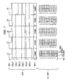
- FIG. 1 is a block diagram showing the configuration of a first embodiment of an information processing device according to the present invention.
- the information processing device of this embodiment is, for example, an information processing device for a mobile phone and is comprised of a semiconductor integrated circuit (LSI) 101 , a camera (CAMERA) 102 , a liquid crystal display (LCD) 103 , a television (TV) 104 , a memory (MEM) 105 , and others.
- LSI semiconductor integrated circuit
- CAMERA camera
- LCD liquid crystal display
- TV television
- MEM memory
- LSI 101 is comprised of a target resource use request arbiter (ARB) 106 , a CPU 107 , a graphics accelerator (GRP) 108 , an image compression/decompression accelerator (VPU) 109 , a camera interface (CEU) 110 , an LCD control circuit (LCDC) 111 , a video interface (VOU) 112 , a circuit module (BLFC) 113 for performing blending and format conversion of images, a circuit module (SOUND) 114 for performing sound processing, a memory interface (MIF) 115 for controlling MEM 105 , and others.
- ARB target resource use request arbiter
- CPU central processing unit
- GPP graphics accelerator
- VPU image compression/decompression accelerator
- CEU camera interface
- LCDC LCD control circuit
- VOU video interface
- BLFC circuit module
- SOUND circuit module
- SOUND circuit module
- MIF memory interface
- CPU 107 GPU 107 , GRP 108 , VPU 109 , BLFC 113 , SOUND 114 , and MIF 115 are connected to ARB 106 , and CAMERA 102 , LCD 103 , and TV 104 are connected to ARB 106 via CEU 110 , LCDC 111 , and VOU 112 , respectively.
- one memory (MEM) 105 (corresponding to a target resource) is shared via the target resource use request arbiter (ARB) 106 (corresponding to a first arbiter) for arbitrating requests from a plurality of circuit modules (corresponding to bus master circuits) such as CPU 107 , GRP 108 , VPU 109 , CEU 110 , LCDC 111 , VOU 112 , BLFC 113 , and SOUND 114 .
- This configuration example has an advantage that, since the distance between the plurality of circuit modules and the memory is short, latency is short and the design is simple.
- the information processing device of this embodiment is provided with a bus, and the plurality of circuit modules (bus master circuits) are connected to the bus. This is true of the following examples.
- FIG. 2 is a block diagram showing the configuration of a second embodiment of the information processing device according to the present invention.
- connection is formed in a hierarchical structure, in which functions equivalent to those of FIG. 1 are realized. More specifically, a plurality of circuit modules such as VPU 109 , CEU 110 , LCDC 111 , VOU 112 , BLFC 113 , and SOUND 114 and a target resource use request arbiter (ARB 2 ) 106 b (corresponding to a second arbiter) are assembled as one circuit module (MIP) 202 (corresponding to a second bus master circuit), and the target resource use request arbiter (ARB 2 ) 106 b arbitrates access requests of the plurality of circuit modules (VPU 109 , CEU 110 , LCDC 111 , VOU 112 , BLFC 113 , and SOUND 114 ) to a target resource use request arbiter (ARB 1 ) 106 a (corresponding to first arbiter).
- the target resource use request arbiter will be also referred to as “arbiter
- Such a hierarchical structure has advantages that the arbiters ARB 1 and ARB 2 can be operated at high frequencies, and simplicity in product deployment can be improved by virtue of assembling highly relevant circuit modules into one IP (MIP).
- MIP IP
- FIG. 3 is a block diagram showing the configuration of a third embodiment of the information processing device according to the present invention.
- the information processing device shown in FIG. 3 is an example of a system configuration including above-mentioned ARB 106 .
- the information processing device shown in FIG. 3 is, for example, an information processing device for a one-chip mobile phone and is comprised of an antenna 305 , RF (Radio Frequency) 306 , a baseband processor (BBP) 304 , an application processor (APP) 301 for performing multimedia processing, a speaker (SP) 307 , a microphone (MP) 308 , various interfaces (IO) 302 , a camera (CAMERA) 102 , LCD 103 , various memories (FLASH 309 , SRAM 310 , SDRAM 303 ), and others.
- RF Radio Frequency
- BBP baseband processor
- APP application processor
- Each of RF 306 , SP 307 , MP 308 , FLASH 309 , SRAM 310 , and APP 301 is connected to BBP 304 , the antenna 305 is connected to RF 306 , and each of IO 302 , CAMERA 102 , LCD 103 , and SDRAM 303 is connected to APP 301 ,
- the application processor (APP) 301 includes the arbiter (ARB) 106 , the image compression/decompression accelerator (VPU) 109 , the circuit module (BLFC) 113 for performing blending and format conversion of images, the camera interface (CEU) 110 , the LCD control circuit (LCDC) 111 , the video interface (VOU) 112 , the memory interface (MIF) 115 , the CPU 107 , DSP 312 , the graphics accelerator (GRP) 108 , and a various peripheral circuit module (PRIPHS) 311 , and the ARB 106 performs access arbitration therebetween.
- ARB arbiter
- Each of the master circuits (MST 1 to MST 3 ) 401 , 402 , and 403 is connected to ARB 106 by signal lines of PRI and MREQB, and TGT 404 is connected thereto by a signal line of TREQB.
- ARB 106 receives target resource use requests via target resource use request origin signal group MREQB from the plurality of master circuits (MST 1 to MST 3 ) 401 , 402 , and 403 , and after arbitration, it transmits a selected request to the target resource (TGT) 404 via target resource use request signal group TREQB.
- the configuration of the target resource use request arbiter (ARB) 106 in this embodiment will be described with reference to FIG. 4 .
- the target resource use request arbiter (ARB) 106 in this embodiment has an arbitration control unit (ARBCTRL) 405 for arbitrating a plurality of requests and a data path unit (DPATH) 406 which transmits the information from a selected master to the target resource (TGT) 404 in response to a result from ARBCTRL 405 .
- ARBCTRL arbitration control unit
- DPATH data path unit
- the arbitration control unit (ARBCTRL) 405 has a first storage unit (ARBCTRLR) 407 for programming the target resource use patterns of each task and an arbitration control logical unit (ARBCTRLL) 408 which determines the task to which a right to use is to be given in accordance with values programmed in the first storage unit (ARBCTRLR) 407 and target resource use history.
- ARBCTRLR first storage unit
- ARBCTRLL arbitration control logical unit
- LVLPRI 410 included in the first storage unit (ARBCTRLR) 407 shows initial values of the priorities of the unit storage blocks (TSKPRIRB) 412 .
- TSKPRIRB unit storage blocks
- FIG. 4 the higher the level in TSKPRIR 409 is, the higher the priority is, and a storage unit for specifying the upper limit thereof is LVLPRIR 411 .
- an integer N is set in LVLPRIR 411 .
- the priorities of M-N th and lower blocks TSKPRIRB 412 are 0.
- a second storage unit (PRIT) 413 is a storage unit in which the initial information of the first storage unit (ARBCTRLR) 407 is inputted and the internal information is changed in accordance with the operation of the information processing device of this embodiment, and similar to the TSKPRIR 409 , it is comprised of a register group and others.
- PRIT 413 is included in ARBCTRLL 408 .
- the configuration is not limited to this, and it may be provided outside ARBCTRLL 408 .
- FIG. 5 is a diagram showing an embodiment of the second storage unit (PRIT) 413 and the relation thereof with the first storage unit (ARBCTRLR) 407 .
- PRIT 413 is a block including PRITB 501 including PTSKID 514 representing a task ID and the number of permitted target resource use requests PNOP 515 , PLVLPRI 502 representing the priorities corresponding thereto, and LVLPRIL 503 for generating PLVLPRI 502 from LVLPRIR 411 in the first storage unit (ARBCTRLR) 407 .
- FIG. 7 is a diagram showing a basic operation of the target resource use request arbiter (ARB) 106 in the first embodiment.
- FIG. 7 shows a case where tasks 0 to 5 share one target resource.
- the upper part SIGS represents signal operations in respective cycles, in which CLK is clocks, REQ_ 0 is a resource use request from the task 0 , REQ_ 1 is a resource use request from the task 1 , REQ_ 2 is a resource use request from the task 2 , REQ_ 3 is a resource use request from the task 3 , REQ_ 4 is a resource use request from the task 4 , REQ_ 5 is a resource use request from the task 5 , and GETT is the tasks which have obtained the right to use the target resource in respective clock cycles.
- the priority of the task 1 drops to the lowest level since a number of processes thereof specified in the third row of the table are completed, and the fourth and the following rows are sequentially raised. At this time, the priorities of the tasks 2 and 3 are maintained without change. Accordingly, even when the timing of the target resource use requests from the masters are varied, the lower limit of the usage amount of the target resource can be maintained for each of the tasks.
- a second one is the method in which the table is explicitly cleared by a program.
- initialization by means of a command dedicated to table initialization and access to a dedicated address has to be implemented.
- the master circuits 401 to 403 output urgency notification signals (PRI signals in FIG. 4 ) of the processing requests for the respective tasks, and the target resource use request arbiter ARB 106 arbitrates the requests by means of the combination of both the urgency notification signals PRI and the above-described method.
- urgency notification signals PRI signals in FIG. 4
- FIG. 9 shows a specific operation of the target resource use request arbiter ARB 106 according to the second embodiment.
- the upper part SIGS represents signal operations in respective cycles.
- CLK is clocks
- REQ_ 0 , 1 , 2 , 3 , 4 , and 5 are target resource use requests from the tasks 0 , 1 , 2 , 3 , 4 , and 5 , respectively
- PRI_ 0 , 1 , 2 , 3 , 4 , and 5 are urgency notification signals to ARB 106 respectively from the tasks 0 , 1 , 2 , 3 , 4 , and 5
- GETT represents the tasks which have obtained the right to use the target resource in respective clock cycles.
- the urgency notification signals PRI are normally 0, and the tasks determine the urgency of the processes and manipulate the urgency. Normally, the value is determined by the relation between the remaining amount and the permissible time of the process.
- a plurality of the circuit modules use the priority signals, and the values of the urgency from the master circuits are determined in the whole system such that the required resource amounts are allocated to the master circuits. Since the value of urgency is different in each LSI, each master circuit can be configured such that the urgency can be set by a storage device in the master circuit or a signal from outside the master circuit.
- urgency 7 is appended to the request from the task 5 .
- This is the value higher than any other priorities of all the tasks in the priority table, and the right to use the target resource is given to the task 5 .
- the operation in the clock cycle ( 4 ) is performed also in the same manner. Concurrently with the completion of this cycle, the priority of the task 5 , which is specified in the fourth row of the priority table, drops to the lowest level, and the tasks of the fifth and the following rows are sequentially raised.
- the proportion specified in TSKPRIR 409 can be readily maintained.
- FIG. 11 shows an example in which performance is improved by use of the method shown in the second embodiment.
- This example shows the results of application execution in which import of camera images, MPEG encoding, image blending, and sound processing are executed in parallel, that is, the number of cycles CYC_FRM required for processing a critical VIDEO frame is shown.
- the target resource is a memory.
- the left side bar RROBIN of the graph is the result before applying the present invention, in which target resource use arbitration by means of the most common round-robin method is performed.
- the right side of the graph that is, NEWARB is the result when the second embodiment is employed.
- wasted cycles IDLE of the target resource can be reduced, and the performance improvement can be achieved.
- the part EXEC in the graph represents the number of cycles where the target resource is effectively utilized.
- the resource usage amount required for each task when real-time applications are executed can be compensated.
- the characteristic thereof is to satisfy the conditions of (1) tolerance against variation in the timing of target resource use requests from the masters is provided, (2) optimization according to the usage manner of the user can be performed, and (3) the operating frequency, the circuit scale, and the like are not largely affected.
- the present invention can be applied to, for example, a system LSI including circuit modules such as CPUs, accelerators for particular processes, and various memory controllers.
Landscapes
- Engineering & Computer Science (AREA)
- Theoretical Computer Science (AREA)
- Physics & Mathematics (AREA)
- General Engineering & Computer Science (AREA)
- General Physics & Mathematics (AREA)
- Bus Control (AREA)
- Memory System (AREA)
Abstract
Description
Claims (6)
Applications Claiming Priority (2)
| Application Number | Priority Date | Filing Date | Title |
|---|---|---|---|
| JP2004365489A JP2006172256A (en) | 2004-12-17 | 2004-12-17 | Information processor |
| JP2004-365489 | 2004-12-17 |
Publications (2)
| Publication Number | Publication Date |
|---|---|
| US20060149884A1 US20060149884A1 (en) | 2006-07-06 |
| US7337251B2 true US7337251B2 (en) | 2008-02-26 |
Family
ID=36641999
Family Applications (1)
| Application Number | Title | Priority Date | Filing Date |
|---|---|---|---|
| US11/304,567 Expired - Lifetime US7337251B2 (en) | 2004-12-17 | 2005-12-16 | Information processing device with priority-based bus arbitration |
Country Status (2)
| Country | Link |
|---|---|
| US (1) | US7337251B2 (en) |
| JP (1) | JP2006172256A (en) |
Cited By (1)
| Publication number | Priority date | Publication date | Assignee | Title |
|---|---|---|---|---|
| CN102112973A (en) * | 2009-06-08 | 2011-06-29 | 松下电器产业株式会社 | Mediation device, mediation system, mediation method, semiconductor integrated circuit, and image processing device |
Families Citing this family (7)
| Publication number | Priority date | Publication date | Assignee | Title |
|---|---|---|---|---|
| FR2894696A1 (en) * | 2005-12-14 | 2007-06-15 | Thomson Licensing Sas | METHOD FOR ACCESSING A DATA TRANSMISSION BUS, DEVICE AND CORRESPONDING SYSTEM |
| US8180990B2 (en) * | 2006-03-10 | 2012-05-15 | Panasonic Corporation | Integrated circuit including a plurality of master circuits transmitting access requests to an external device and integrated circuit system including first and second interated circuits each including a plurality of master circuits transmitting access requests |
| US20090125664A1 (en) * | 2006-04-04 | 2009-05-14 | Takatoshi Ueyama | System controller |
| US8126415B2 (en) * | 2008-06-19 | 2012-02-28 | Broadcom Corporation | Method and system for clock synchronization in a global navigation satellite system (GNSS) receiver |
| JP5380322B2 (en) * | 2010-02-17 | 2014-01-08 | 京セラドキュメントソリューションズ株式会社 | Memory master device |
| US8706936B2 (en) | 2011-11-14 | 2014-04-22 | Arm Limited | Integrated circuit having a bus network, and method for the integrated circuit |
| US10303631B2 (en) * | 2016-03-17 | 2019-05-28 | International Business Machines Corporation | Self-moderating bus arbitration architecture |
Citations (10)
| Publication number | Priority date | Publication date | Assignee | Title |
|---|---|---|---|---|
| US5151994A (en) * | 1989-11-13 | 1992-09-29 | Hewlett Packard Company | Distributed fair arbitration system using separate grant and request lines for providing access to data communication bus |
| US5862355A (en) * | 1996-09-12 | 1999-01-19 | Telxon Corporation | Method and apparatus for overriding bus prioritization scheme |
| US5884051A (en) * | 1997-06-13 | 1999-03-16 | International Business Machines Corporation | System, methods and computer program products for flexibly controlling bus access based on fixed and dynamic priorities |
| US6411218B1 (en) * | 1999-01-22 | 2002-06-25 | Koninklijke Philips Electronics N.V. | Priority-encoding device selection using variable arbitrary rankings |
| US20020133654A1 (en) * | 2001-02-13 | 2002-09-19 | Hitoshi Yamamoto | Method and apparatus for bus arbitration capable of effectively altering a priority order |
| US6467002B1 (en) * | 1999-10-19 | 2002-10-15 | 3Com Corporation | Single cycle modified round-robin arbitration with embedded priority |
| US20030167294A1 (en) * | 2002-03-01 | 2003-09-04 | Darren Neuman | System and method for arbitrating clients in a hierarchical real-time dram system |
| US6704821B2 (en) * | 2000-07-05 | 2004-03-09 | Stmicroelectronics S.R.L. | Arbitration method and circuit architecture therefore |
| US7073003B2 (en) * | 2002-11-27 | 2006-07-04 | Samsung Electronics, Co., Ltd. | Programmable fixed priority and round robin arbiter for providing high-speed arbitration and bus control method therein |
| US7130943B2 (en) * | 2004-09-30 | 2006-10-31 | Freescale Semiconductor, Inc. | Data processing system with bus access retraction |
Family Cites Families (3)
| Publication number | Priority date | Publication date | Assignee | Title |
|---|---|---|---|---|
| JPH0381856A (en) * | 1989-08-25 | 1991-04-08 | Hitachi Ltd | Data transfer control method |
| JPH04363748A (en) * | 1991-03-12 | 1992-12-16 | Toshiba Corp | Priority control method and its circuit |
| JPH05274254A (en) * | 1992-03-06 | 1993-10-22 | Nec Corp | Bus arbiter circuit |
-
2004
- 2004-12-17 JP JP2004365489A patent/JP2006172256A/en active Pending
-
2005
- 2005-12-16 US US11/304,567 patent/US7337251B2/en not_active Expired - Lifetime
Patent Citations (10)
| Publication number | Priority date | Publication date | Assignee | Title |
|---|---|---|---|---|
| US5151994A (en) * | 1989-11-13 | 1992-09-29 | Hewlett Packard Company | Distributed fair arbitration system using separate grant and request lines for providing access to data communication bus |
| US5862355A (en) * | 1996-09-12 | 1999-01-19 | Telxon Corporation | Method and apparatus for overriding bus prioritization scheme |
| US5884051A (en) * | 1997-06-13 | 1999-03-16 | International Business Machines Corporation | System, methods and computer program products for flexibly controlling bus access based on fixed and dynamic priorities |
| US6411218B1 (en) * | 1999-01-22 | 2002-06-25 | Koninklijke Philips Electronics N.V. | Priority-encoding device selection using variable arbitrary rankings |
| US6467002B1 (en) * | 1999-10-19 | 2002-10-15 | 3Com Corporation | Single cycle modified round-robin arbitration with embedded priority |
| US6704821B2 (en) * | 2000-07-05 | 2004-03-09 | Stmicroelectronics S.R.L. | Arbitration method and circuit architecture therefore |
| US20020133654A1 (en) * | 2001-02-13 | 2002-09-19 | Hitoshi Yamamoto | Method and apparatus for bus arbitration capable of effectively altering a priority order |
| US20030167294A1 (en) * | 2002-03-01 | 2003-09-04 | Darren Neuman | System and method for arbitrating clients in a hierarchical real-time dram system |
| US7073003B2 (en) * | 2002-11-27 | 2006-07-04 | Samsung Electronics, Co., Ltd. | Programmable fixed priority and round robin arbiter for providing high-speed arbitration and bus control method therein |
| US7130943B2 (en) * | 2004-09-30 | 2006-10-31 | Freescale Semiconductor, Inc. | Data processing system with bus access retraction |
Cited By (2)
| Publication number | Priority date | Publication date | Assignee | Title |
|---|---|---|---|---|
| CN102112973A (en) * | 2009-06-08 | 2011-06-29 | 松下电器产业株式会社 | Mediation device, mediation system, mediation method, semiconductor integrated circuit, and image processing device |
| CN102112973B (en) * | 2009-06-08 | 2016-04-13 | 松下知识产权经营株式会社 | Conditioning unit, coherent system, coordination approach, SIC (semiconductor integrated circuit) and image processing apparatus |
Also Published As
| Publication number | Publication date |
|---|---|
| US20060149884A1 (en) | 2006-07-06 |
| JP2006172256A (en) | 2006-06-29 |
Similar Documents
| Publication | Publication Date | Title |
|---|---|---|
| US8533403B1 (en) | Arbitration unit for memory system | |
| US7363406B2 (en) | Dynamic access scheduling memory controller | |
| US20070271441A1 (en) | Availability of space in a RISC microprocessor architecture | |
| US10055369B1 (en) | Systems and methods for coalescing interrupts | |
| US9201821B2 (en) | Interrupt timestamping | |
| US8694705B2 (en) | Information processing device | |
| US10255218B1 (en) | Systems and methods for maintaining specific ordering in bus traffic | |
| US7337251B2 (en) | Information processing device with priority-based bus arbitration | |
| US9035961B2 (en) | Display pipe alternate cache hint | |
| US8922571B2 (en) | Display pipe request aggregation | |
| US8972693B2 (en) | Hardware managed allocation and deallocation evaluation circuit | |
| US8478946B2 (en) | Method and system for local data sharing | |
| JP6396715B2 (en) | Data processing device | |
| US8560784B2 (en) | Memory control device and method | |
| US8856459B1 (en) | Matrix for numerical comparison | |
| Sousa et al. | Runtime reconfigurable bus arbitration for concurrent applications on heterogeneous MPSoC architectures | |
| US7080176B2 (en) | Bus control device and information processing system | |
| US20110197008A1 (en) | Card host lsi and set device including the lsi | |
| US12093541B1 (en) | Temperature-based bandwidth compensation for memory traffic | |
| US10740150B2 (en) | Programmable state machine controller in a parallel processing system | |
| CN117234674A (en) | Methods for performing task scheduling and related products | |
| JP2005346513A (en) | Semiconductor device | |
| US5799160A (en) | Circuit and method for controlling bus arbitration | |
| US12596658B2 (en) | Mechanisms for arbitrating among packets in one or more co-packaged integrated circuits | |
| US12591525B2 (en) | Mechanisms for arbitrating among packets in hierarchical arbitration architecture |
Legal Events
| Date | Code | Title | Description |
|---|---|---|---|
| AS | Assignment |
Owner name: RENESAS TECHNOLOGY CORP., JAPAN Free format text: ASSIGNMENT OF ASSIGNORS INTEREST;ASSIGNORS:SAEN, MAKOTO;UEDA, HIROSHI;YAMAMOTO, EIJI;REEL/FRAME:017654/0557 Effective date: 20051101 |
|
| STCF | Information on status: patent grant |
Free format text: PATENTED CASE |
|
| FEPP | Fee payment procedure |
Free format text: PAYOR NUMBER ASSIGNED (ORIGINAL EVENT CODE: ASPN); ENTITY STATUS OF PATENT OWNER: LARGE ENTITY |
|
| AS | Assignment |
Owner name: RENESAS ELECTRONICS CORPORATION, JAPAN Free format text: CHANGE OF NAME;ASSIGNOR:NEC ELECTRONICS CORPORATION;REEL/FRAME:024953/0404 Effective date: 20100401 Owner name: NEC ELECTRRONICS CORPORATION, JAPAN Free format text: MERGER;ASSIGNOR:RENESAS TECHNOLOGY CORP.;REEL/FRAME:024933/0869 Effective date: 20100401 |
|
| FPAY | Fee payment |
Year of fee payment: 4 |
|
| FPAY | Fee payment |
Year of fee payment: 8 |
|
| AS | Assignment |
Owner name: RENESAS ELECTRONICS CORPORATION, JAPAN Free format text: CHANGE OF ADDRESS;ASSIGNOR:RENESAS ELECTRONICS CORPORATION;REEL/FRAME:044928/0001 Effective date: 20150806 |
|
| MAFP | Maintenance fee payment |
Free format text: PAYMENT OF MAINTENANCE FEE, 12TH YEAR, LARGE ENTITY (ORIGINAL EVENT CODE: M1553); ENTITY STATUS OF PATENT OWNER: LARGE ENTITY Year of fee payment: 12 |