US7315993B2 - Verification of RRAM tiling netlist - Google Patents
Verification of RRAM tiling netlist Download PDFInfo
- Publication number
- US7315993B2 US7315993B2 US10/999,468 US99946804A US7315993B2 US 7315993 B2 US7315993 B2 US 7315993B2 US 99946804 A US99946804 A US 99946804A US 7315993 B2 US7315993 B2 US 7315993B2
- Authority
- US
- United States
- Prior art keywords
- net
- cell
- rram
- nets
- netlist
- Prior art date
- Legal status (The legal status is an assumption and is not a legal conclusion. Google has not performed a legal analysis and makes no representation as to the accuracy of the status listed.)
- Expired - Fee Related, expires
Links
Images


Classifications
-
- G—PHYSICS
- G06—COMPUTING OR CALCULATING; COUNTING
- G06F—ELECTRIC DIGITAL DATA PROCESSING
- G06F30/00—Computer-aided design [CAD]
- G06F30/30—Circuit design
- G06F30/32—Circuit design at the digital level
- G06F30/33—Design verification, e.g. functional simulation or model checking
Definitions
- the present invention generally relates to the field of integrated circuits, particularly to verification of a RRAM tiling netlist.
- Platform-based IC (integrated circuit) design is a powerful concept for coping with the increased pressure on time-to-market, design and manufacturing costs encountered in the current IC market.
- a platform is a large-scale, high-complexity semiconductor device that includes one or more of the following elements: (1) memory; (2) a customizable array of transistors; (3) an IP (intellectual property) block; (4) a processor, e.g., an ESP (embedded standard product); (5) an embedded programmable logic block; and (6) interconnect.
- RapidChipTM developed by LSI Logic Corp. is an instance of a platform. The basic idea behind the platform-based design is to avoid designing and manufacturing a chip from scratch. Some portion of the chip's architecture is predefined for a specific type of application. Through extensive design reuse, the platform-based design may provide faster time-to-market and reduced design cost.
- a prefabrication step a slice is built on a wafer.
- a slice is a pre-manufactured chip in which all silicon layers have been built, leaving the metal layers or top metal layers to be completed with the customer'unique IP.
- RapidSliceTM developed by LSI Logic Corp. is an instance of a slice.
- One or more slices may be built on a single wafer. It is understood that a slice may include one or more bottom metal layers or may include no metal layers at all.
- portions of the metal layers are pre-specified to implement the pre-defined blocks of the platform and the diffusion processes are carried out in a wafer fab.
- the base characteristics in terms of the IP, the processors, the memory, the interconnect, the programmable logic and the customizable transistor array, are all pre-placed in the design and pre-diffused in the slice.
- a slice is still fully decoupled because the customer has not yet introduced the function into the slice.
- the customer-designed function is merged with the pre-defined blocks and the metal layers (or late-metal components) are laid down, which couple the elements that make up the slice built in the wafer fab, and the customizable transistor array is configured and given its characteristic function.
- early-metal steps may be part of the pre-fabricated slice to reduce the time and cost of the customization step, resulting in a platform which is more coupled and specific. It is understood that a prefabrication step and a customization step may be performed in different foundries. For example, a slice may be manufactured in one foundry. Later, in a customization step, the slice may be pulled from inventory and metalized, which gives the slice its final product characteristics in a different foundry.
- a slice such as RapidSliceTM may contain several RRAMs (Reconfigurable RAMs, or Redundant RAMs, or RapidSliceTM RAMs). Each RRAM is a set of memories of the same type that are placed compactly. RRAMs include built-in testing and self-repairing components. While being mapped to a slice, each customer memory (i.e., a memory of customer design) is presented as a tiling netlist, which is a netlist including RRAM memories, flip-flops and/or logical cells.
- a RRAM tiling netlist is a netlist that represents a unity of the netlists that correspond to all customer memories mapped to one given RRAM.
- the present invention provides a method of verification of a RRAM tiling netlist.
- the method may include steps as follows. Properties “memory_number”, “clock_number” and “netlist_part” of all nets and cells of a RRAM tiling netlist are set to a value 0.
- a boolean function 0 is assigned to all ground nets of the RRAM tiling netlist, and a boolean function 1 is assigned to all power nets of the RRAM tiling netlist.
- the RRAM tiling netlist is verified for a customer memory Mem k as follows. Inputs of the RRAM tiling netlist that correspond to inputs of the memory Mem k are analyzed, and a boolean variable is assigned to each of the inputs of the RRAM. Boolean functions are evaluated and assigned to nets encountered when moving around the RRAM tiling netlist starting from inputs toward memories and flip-flops, and property “netlist_part” of all encountered nets and cells is set to value 1, MARKED_CELLS being a set of encountered cells that are not evaluated yet, PROCESSED_CELLS being a set of encountered cells that are already evaluated.
- Boolean functions are evaluated and assigned to nets encountered when moving around the RRAM tiling netlist starting from outputs of memories and flip-flops of the RRAM tiling netlist toward outputs of the RRAM tiling netlist, and property “netlist_part” of all encountered nets and cells to is set to a value 2.
- the outputs of the RRAM tiling netlist that correspond to outputs of the memory Mem k are analyzed, and it is ensured that boolean functions of the outputs of the RRAM tiling netlist are evaluated and correct.
- the present invention provides a method or algorithm of verification of a RRAM tiling netlist.
- the present invention uses RRAMs that contain only 222 memories and assumes customer memories are also of type 222 .
- the 222 memory is a memory that may process 2 read/write operations in parallel. These 2 operations may be driven by 2 different clocks.
- Each 222-memory of a width W and a capacity CAP has the following set of ports:
- the inputs CLKA and CLKB are clock inputs of the memory.
- the ports ENA, DIA[0:W ⁇ 1], WEA[0:W ⁇ 1], AADR[0:LCAP ⁇ 1] and DOA[0:W ⁇ 1] correspond to the clock CLKA.
- the ports ENB, DIB[0:W ⁇ 1], WEB[0:W ⁇ 1], BADR[0:LCAP ⁇ 1] and DOB[0:W ⁇ 1] correspond to the clock CLKB.
- the inputs ENA and ENB are enable inputs.
- the inputs DIA and DIB are data inputs
- WEA and WEB are write enable inputs
- AADR and BADR are address inputs
- the outputs DOA and DOB are data outputs.
- Mem 1 , Mem 2 , . . . , Mem N be customer memories mapped to the RRAM, where N is the number of these memories.
- customer memory ports are correspondingly defined. For each port PORT of each memory Mem k , the corresponding net NET(PORT, Mem k ) of the RRAM tiling netlist is defined.
- the present algorithm of verification deals with construction and comparison of logical (or boolean) functions.
- the construction of boolean functions may be reduced to applying operations (e.g., OR, AND, NAND, NOR, and the like) to existing boolean functions.
- the BDD (binary decision diagram) technique may be used to effectively organize the boolean function comparison and the boolean function operations.
- the present algorithm uses 2 sets of RRAM tiling netlist cells: MARKED_CELLS and PROCESSED_CELLS. During the algorithm execution, cells of the RRAM tiling netlist may be added to or removed from these two sets.
- Each net (including inputs and outputs) and each cell of the RRAM tiling netlist has 3 properties: “memory_number”, “clock_number” and “netlist_part”.
- the property “memory_number” may take values 0, 1, 2, . . . , N and indicates the number of customer memory to which the given net/cell corresponds (the value 0 is used if there is no corresponding memory).
- the property “clock_number” may take values 0, 1, 2 and represents the number of clock (CLKA ⁇ 1, CLKB- 2 ) that drives the given net/cell (the value 0 is used if there is no clock that drives a net/cell).
- the property “netlist_part” may take values 0, 1, 2 and is a special property that is used for understanding the position of the given net/cell in the RRAM tiling netlist.
- the value 1 is used for the property “netlist_part” if the given net/cell lies on a logical path that connects a RRAM tiling netlist input with an input of an internal RRAM memory or flip-flop.
- the value 2 is used if the given net/cell lies on a logical path that connects an output of an internal RRAM memory or flip-flop with a RRAM tiling netlist output.
- boolean functions are assigned to nets of the RRAM tiling netlist. If no boolean function is assigned to a net, then the net is defined as not evaluated. If all the nets connected to inputs of a cell of a RRAM tiling netlist are already evaluated, then the cell is defined as ready for evaluation. If all the nets connected to outputs of a cell of a RRAM tiling netlist are evaluated, then the cell is defined as evaluated
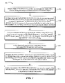
- the method 100 may include steps as follows.
- properties “memory_number”, “clock_number” and “netlist_part” of all nets and cells of a RRAM tiling netlist are set to a value 0.
- a boolean function 0 is assigned to all ground nets of the RRAM tiling netlist, and a boolean function 1 is assigned to all power nets of the RRAM tiling netlist 104 .
- a message indicating verification of the RRAM tiling netlist is successfully is output 108 .
- the method 200 may include steps as follows.
- inputs of the RRAM tiling netlist that correspond to inputs of the memory Mem k are analyzed, and a boolean variable is assigned to each of the inputs of the RRAM.
- the following sub-steps are implemented:
- boolean functions are evaluated and assigned to nets encountered when moving around the RRAM tiling netlist starting from inputs toward memories and flip-flops, and property “netlist_part” of all encountered nets and cells is set to value 1, MARKED_CELLS being a set of encountered cells that are not evaluated yet, PROCESSED_CELLS being a set of encountered cells that are already evaluated.
- the following sub-steps are implemented:
- step 204 if the cell CELL is a flip-flop, then consider the boolean function assigned to the net connected to the clock input of flip-flop CELL. If this boolean function is not equal to boolean the variable “clock”, then output a message indicating that the verification is failed.
- step 206 one may find equivalent pairs of bits (x a,b ) stored in the memory Mem k and bits (y i,j ) stored in internal memories of the RRAM tiling netlist, and assign a “dummy” variable z Z — MEM — NUM to a bit y i,j of the internal memories when the bit y i,j has no equivalent bit in the memory Mem k .
- All the internal RRAM memories M from the set PROCESSED_CELLS may be examined. For each examined memory M, one may denote W M as a width of the memory M, CAP M as a capacity of the memory M, LCAP M as the minimal integer number that is not less than log 2 CAP M .
- the following sub-steps are implemented:
- boolean functions are assigned to nets connected to outputs of internal RRAM memories and flip-flops sets.
- all the flip-flops FF from the set PROCESSED_CELLS are examined.
- For each flip-flop FF consider two nets D_NET and Q_NET connected to data input and data output of the flip-flop.
- boolean functions are evaluated and assigned to nets encountered when moving around the RRAM tiling netlist starting from outputs of memories and flip-flops of the RRAM tiling netlist toward outputs of the RRAM tiling netlist, and property “netlist_part” of all encountered nets and cells to is set to a value 2.
- the following sub-steps are implemented:
- the outputs of the RRAM tiling netlist that correspond to outputs of the memory Mem k are analyzed, and it is ensured that boolean functions of the outputs of the RRAM tiling netlist are evaluated and correct.
- i 0, 1, . . . , W k ⁇ 1. For each i, consider two nets of the RRAM tiling netlist: NET(DOA[i], Mem k ) and NET(DOB[i], Mem k ).
- At least one of these nets is not the output of the RRAM tiling netlist, or at least one of them has the value of the property “memory_number” not equal to k, or at least one of them has the value of the property “netlist_part” not equal to 2, or at least one of them is not evaluated, or the net NET(DOA[i], Mem k ) has the value of the property “clock_number” not equal to 1, or the net NET(DOB[i], Mem k ) has the value of the property “clock_number” not equal to 2, a message indicating that the verification is failed is output. After that, one may consider the boolean functions that are assigned to these two nets.
- Such a software package may be a computer program product which employs a computer-readable medium including stored computer code which is used to program a computer to perform the disclosed function and process of the present invention.
- the computer-readable medium may include, but is not limited to, any type of conventional floppy disks, optical disks, CD-ROMS, magneto-optical disks, ROMs, RAMs, EPROMs, EEPROMs, magnetic or optical cards, or any other suitable media for storing electronic instructions.
Landscapes
- Engineering & Computer Science (AREA)
- Computer Hardware Design (AREA)
- Physics & Mathematics (AREA)
- Theoretical Computer Science (AREA)
- Evolutionary Computation (AREA)
- Geometry (AREA)
- General Engineering & Computer Science (AREA)
- General Physics & Mathematics (AREA)
- Design And Manufacture Of Integrated Circuits (AREA)
Abstract
Description
-
- inputs CLKA, ENA, DIA[0:W−1], WEA[0:W−1], AADR[0:LCAP−1]; outputs DOA[0:W−1]; and
- inputs CLKB, ENB, DIB[0:W−1], WEB[0:W−1], BADR[0:LCAP−1]; outputs DOB[0:W−1];
where LCAP is the minimal integer number that is not less than log2CAP.
-
- (i) Define the boolean variables that are used for the construction of boolean functions and assigned to RRAM tiling netlist nets as follows: “clock”, “enable”, “addrt”, “wes”, “dis”, “xs,r”, s=0, 1, . . . , Wk−1, t=0, 1, . . . , LCAPk−1, r=0, 1, . . . , CAPk−1. Define infinite set of variables “z1”, “z2”, “z3”, . . . . Set Z_VAR_NUM=0, where Z_VAR_NUM is the number of variables “z” that are used by the present algorithm;
- (ii) Clean sets MARKED_CELLS and PROCESSED_CELLS;
- (iii) Examine all the nets NET(A_INPUT, Memk) of the RRAM tiling netlist for each input A_INPUT of memory Memk driven by clock CLKA (these are inputs CLKA, ENA, DIA[0:Wk−1], WEA[0:Wk−1], AADR[0:LCAPk−1]). For each examined net NET, check if the value of its property “memory_number” is 0. If the value is not 0, then output a message indicating that verification is failed; otherwise, set properties of the net NET: memory_number=k, clock_number=1, netlist_part=1;
- (iv) Examine all the nets NET(B_INPUT, Memk) of the RRAM tiling netlist for each input B_INPUT of memory Memk driven by clock CLKB (these are inputs CLKB, ENB, DIB[0:Wk−1], WEB[0:Wk−1], BADR[0:LCAPk−1]). For each examined net NET, check if the value of its property “memory_number” is 0. If the value is not 0, then output a message indicating that verification is failed; otherwise, set properties of the net NET: memory_number=k, clock_number=2, netlist_part=1; and
- (v) Assign the boolean variable “clock” to the nets NET(CLKA, Memk) and NET(CLKB, Memk). Assign the boolean variable “enable” to nets NET(ENA, Memk) and NET(ENB, Memk). Assign the boolean variable “dis” to the nets NET(DIA[s], Memk) and NET(DIB[s], Memk) and assign the boolean variable “wes” to the nets NET(WEA[s], Memk) and NET(WEB[s], Memk), where s=0, 1, . . . , Wk−1. Assign the boolean variable “addrt” to the nets NET(AADR[t], Memk) and NET(BADR[t], Memk), where t=0, 1, . . . , LCAPk−1. If one of considered nets is not an input of the RRAM tiling netlist, then a message indicating that the verification is failed is output.
-
- (i) For each net NET examined at the
step 202, consider the cells whose inputs are connected to the net NET and append these cells to the set MARKED_CELLS; - (ii) While the set MARKED_CELLS is not empty and there are at least one cell in this set that are ready for evaluation, implementing the following sub-steps:
- i) Take (and remove) a cell CELL that is ready for evaluation from the set MARKED_CELLS, and append this cell to the set PROCESSED_CELLS;
- ii) Examine all the nets INP_NET connected to inputs of the cell CELL;
- iii) Check if the values of property “memory_number” of nets INP_NET are 0 or k. If the values are neither 0 nor k, then output a message indicating that the verification is failed; otherwise, set the property of the cell CELL: memory_number=k; and
- iv) Check if the values of property “netlist_part” of nets INP_NET are 0 or 1. If the values are neither 0 or 1, then output a message indicating that the verification is failed; otherwise, set the property of the cell CELL: netlist_part=1; and
- (iii) If the set MARKED_CELLS is not empty after implementing the foregoing sub-step (ii) of the step 204 (thus it contains only the cells that are not ready for evaluation), output a message indicating that the verification is failed.
- (i) For each net NET examined at the
-
- (i) Consider the boolean functions assigned to the nets connected to the clock inputs CLKA and CLKB of the memory CELL. If at least one of these boolean functions is not equal to the boolean variable “clock”, then output a message indicating that the verification is failed;
- (ii) Consider the nets connected to inputs CLKA, ENA, DIA, WEA, AADR of the memory CELL. If at least one of these nets has the property clock_number=2, output a message indicating that the verification is failed;
- (iii) Consider the nets connected to inputs CLKB, ENB, DIB, WEB, BADR of the memory CELL. If at least one of these nets has the property clock_number=1, output a message indicating that the verification is failed; and
- (iv) Consider nets connected to the following pairs of memory CELL inputs: ENA and ENB, DIA[s] and DIB[s], WEA[s] and WEB[s], AADR[t] and BADR[t], where s=0, 1, . . . , WCELL−1, t=0, 1, . . . , where LCAPCELL−1, WCELL is a width of memory CELL, CAPCELL is a capacity of the memory CELL, and LCAPCELL is the minimal integer number that is no less than log2CAPCELL. If there is at least one pair of nets that have the different boolean functions, output a message indicating that the verification is failed.
-
- (i) Examine all the outputs of a logical cell CELL and the nets OUT_NET connected to these outputs;
- (ii) Set the values of properties of the examined net OUT_NET: memory_number=k, netlist_part=1, and “clock_number” being the same as the “clock_number” of the cell CELL;
- (iii) Evaluate the function of the examined net OUT_NET and assign this function to this net OUT_NET. This may be implemented by applying the boolean operation determined by the cell CELL to the boolean functions assigned to nets connected to inputs of the cell CELL (For example, if the cell CELL is of a type AND2, and the boolean functions assigned to nets connected to inputs of this cell are F1 and F2, then the boolean function F1 & F2 is assigned to the net OUT_NET connected to the output of cell); and
- (iv) Consider the cells whose inputs are connected to the examined net OUT_NET and append these cells to the set MARKED_CELLS.
-
- (i) For each i=0, 1, . . . , WM, and each j=0, 1, . . . , CAPM−1, define the boolean function yi,j, as follows:
- i) Define three boolean functions F_ADRi,j=F(ENA)&(AADR==j)&(addr<CAPk), F_WEi,j=F(WEA[i])&F_ADRi,j and F_DIi,j=F(DIA[i])&F_WEi,j, where F(ENA), F(WEA[i]) and F(DIA[i]) are the boolean functions assigned to the nets connected to the inputs ENA, WEA[i] and DIA[i] of the memory M, respectfully. The boolean function (addr<CAPk) is the function that depends from the boolean variables addr0, addr1, . . . , addrLCAPk−1 and takes the
value 1 if and only if the number addr (those binary presentation is addrLCAPk−1, addrLCAPk-2, . . . , addr1, addr0) is less than the capacity CAPk of the memory Memk. The boolean function (AADR==j) may be presented as (AADR==j)=(F(AADR[0])==j0)&(F(AADR[1])==j1)& . . . &(F(AADR[q])==jq), where F(AADR[s]) is the boolean function assigned to the net connected to the input AADR[s] of the memory M, s=0, 1, . . . , q, q=LCAPM−1, and jqjq−1 . . . j1j0 is the binary presentation of the number j; - ii) One may try to find the pair (a,b) of integer numbers such that 0<=a<Wk, 0<=b<CAPk−1, and that F_WEi,j=enable &wea&(addr==b) and F_DIi,j=enable &wea&(addr==b)&dia, where the boolean function (addr==b) may be presented as (addr==b)=(addr0==b0)&(addr1==b1)& . . . &(addrq==bq), where q=LCAPk−1, and bqbq−1. . . b1b0 is the binary presentation of the number b; and
- iii) If the numbers a and b have been successfully found, then assign yi,j=xa,b; otherwise, assign yi,j=zZ
— VAR— NUM and set Z_VAR_NUM=Z_VAR_NUM+ 1;
- i) Define three boolean functions F_ADRi,j=F(ENA)&(AADR==j)&(addr<CAPk), F_WEi,j=F(WEA[i])&F_ADRi,j and F_DIi,j=F(DIA[i])&F_WEi,j, where F(ENA), F(WEA[i]) and F(DIA[i]) are the boolean functions assigned to the nets connected to the inputs ENA, WEA[i] and DIA[i] of the memory M, respectfully. The boolean function (addr<CAPk) is the function that depends from the boolean variables addr0, addr1, . . . , addrLCAPk−1 and takes the
- (ii) Examine each i=0, 1, . . . , WM−1. Denote A_OUT_NET and B_OUT_NET to be nets that are connected to the memory M outputs DOA[i] and DOB[i];
- (iii) Set the values of properties for both nets: memory_number=k, netlist_part=2. For the net A_OUT_NET, set clock_number=1; for the net B_OUT_NET, set clock_number=2;
- (iv) Assign the following boolean functions to both nets A_OUT_NET and B_OUT_NET: ((yi,0& F_ADRi,0)|(yi,1& F_ADRi,1)| . . . |(yi,q& F_ADRi,q)), where q=CAPM−1; and
- (i) For each i=0, 1, . . . , WM, and each j=0, 1, . . . , CAPM−1, define the boolean function yi,j, as follows:
-
- (i) While the set MARKED_CELLS is not empty and there are some cells in this set that are ready for evaluation, implementing the following sub-steps:
- i) Take (and remove) a cell CELL that is ready for evaluation from the set MARKED_CELLS. Append this cell to the set PROCESSED_CELLS. If the cell CELL is not a logical cell (thus the cell CELL is a memory or a flip-flop), then output a message indicating that the verification is failed;
- ii) Examine all the nets INP_NET connected to input of the cell CELL;
- iii) Check if the values of property “memory_number” of nets INP_NET are 0 or k. If the values are neither 0 nor k, then output a message indicating that the verification is failed; otherwise, set the property of the cell CELL: memory_number=k;
- iv) Check if the values of property “netlist_part” of nets INP_NET are 0 or 2. If the values are neither 0 nor 2, then output a message indicating that the verification is failed; otherwise, set the property of the cell CELL: netlist_part=2;
- v) Consider the values of property “clock_number” of nets INP_NET. If both
values only value 0 is presented; - vi) Examine all the outputs of the logical cell CELL and the nets OUT_NET connected to these outputs;
- vii) Set the values of properties of the examined net OUT_NET: memory_number=k, netlist_part=2, “clock_number” being the same as the “clock_number” of the cell CELL;
- viii) Evaluate the function of the examined net OUT_NET and assign this function to this net OUT_NET. This may be done by applying the boolean operation determined by the cell CELL to the boolean functions assigned to nets connected to inputs of the cell CELL; and
- ix) Consider the cells whose inputs are connected to the examined net OUT_NET and append these cells to the set MARKED_CELLS; and
- (ii) If the set MARKED_CELLS is not empty after implementing the foregoing sub-step (i) of the step 210 (thus, it contains only the cells that are not ready for evaluation), a message indicating that the verification is failed is output.
- (i) While the set MARKED_CELLS is not empty and there are some cells in this set that are ready for evaluation, implementing the following sub-steps:
Claims (20)
Priority Applications (1)
| Application Number | Priority Date | Filing Date | Title |
|---|---|---|---|
| US10/999,468 US7315993B2 (en) | 2004-11-30 | 2004-11-30 | Verification of RRAM tiling netlist |
Applications Claiming Priority (1)
| Application Number | Priority Date | Filing Date | Title |
|---|---|---|---|
| US10/999,468 US7315993B2 (en) | 2004-11-30 | 2004-11-30 | Verification of RRAM tiling netlist |
Publications (2)
| Publication Number | Publication Date |
|---|---|
| US20060117281A1 US20060117281A1 (en) | 2006-06-01 |
| US7315993B2 true US7315993B2 (en) | 2008-01-01 |
Family
ID=36568583
Family Applications (1)
| Application Number | Title | Priority Date | Filing Date |
|---|---|---|---|
| US10/999,468 Expired - Fee Related US7315993B2 (en) | 2004-11-30 | 2004-11-30 | Verification of RRAM tiling netlist |
Country Status (1)
| Country | Link |
|---|---|
| US (1) | US7315993B2 (en) |
Cited By (1)
| Publication number | Priority date | Publication date | Assignee | Title |
|---|---|---|---|---|
| US20070044053A1 (en) * | 2005-08-17 | 2007-02-22 | Alexander Andreev | Multimode delay analyzer |
Families Citing this family (3)
| Publication number | Priority date | Publication date | Assignee | Title |
|---|---|---|---|---|
| US7200826B2 (en) * | 2004-11-30 | 2007-04-03 | Lsi Logic Corporation | RRAM memory timing learning tool |
| US8516417B2 (en) | 2009-08-07 | 2013-08-20 | International Business Machines Corporation | Method and system for repartitioning a hierarchical circuit design |
| CN103942079B (en) * | 2014-05-12 | 2017-06-20 | 张家港市复安电子科技有限公司 | Netlist builds and loading method and its system |
Citations (34)
| Publication number | Priority date | Publication date | Assignee | Title |
|---|---|---|---|---|
| US5680332A (en) * | 1995-10-30 | 1997-10-21 | Motorola, Inc. | Measurement of digital circuit simulation test coverage utilizing BDDs and state bins |
| US5734798A (en) * | 1995-12-01 | 1998-03-31 | Hewlett-Packard Co. | Method and apparatus for extracting a gate modeled circuit from a fet modeled circuit |
| US5812414A (en) * | 1988-10-05 | 1998-09-22 | Quickturn Design Systems, Inc. | Method for performing simulation using a hardware logic emulation system |
| US5910958A (en) * | 1991-08-14 | 1999-06-08 | Vlsi Technology, Inc. | Automatic generation of test vectors for sequential circuits |
| US5940603A (en) * | 1993-06-24 | 1999-08-17 | Quickturn Design Systems, Inc. | Method and apparatus for emulating multi-ported memory circuits |
| US6078735A (en) * | 1997-09-29 | 2000-06-20 | Xilinx, Inc. | System and method for generating memory initialization logic in a target device with memory initialization bits from a programmable logic device |
| US6115300A (en) * | 1998-11-03 | 2000-09-05 | Silicon Access Technology, Inc. | Column redundancy based on column slices |
| US6151568A (en) * | 1996-09-13 | 2000-11-21 | Sente, Inc. | Power estimation software system |
| US6181614B1 (en) * | 1999-11-12 | 2001-01-30 | International Business Machines Corporation | Dynamic repair of redundant memory array |
| US6195776B1 (en) * | 1998-11-02 | 2001-02-27 | Synopsys, Inc. | Method and system for transforming scan-based sequential circuits with multiple skewed capture events into combinational circuits for more efficient automatic test pattern generation |
| US6249901B1 (en) * | 1996-12-13 | 2001-06-19 | Legend Design Technology, Inc. | Memory characterization system |
| US6295627B1 (en) * | 1998-12-04 | 2001-09-25 | Cypress Semiconductor Corporation | Method and apparatus for the automated design of memory devices |
| US6345379B1 (en) * | 1994-06-03 | 2002-02-05 | Synopsys, Inc. | Method and apparatus for estimating internal power consumption of an electronic circuit represented as netlist |
| US6523155B1 (en) * | 1998-11-17 | 2003-02-18 | Jeffrey Joseph Ruedinger | Method for partitioning a netlist into multiple clock domains |
| US6618311B1 (en) * | 2002-02-12 | 2003-09-09 | Artisan Components, Inc. | Zero power fuse sensing circuit for redundancy applications in memories |
| US20030172055A1 (en) * | 2002-03-08 | 2003-09-11 | Mentor Graphics Corporation | Array transformation in a behavioral synthesis tool. |
| US6667917B1 (en) * | 2001-06-15 | 2003-12-23 | Artisan Components, Inc. | System and method for identification of faulty or weak memory cells under simulated extreme operating conditions |
| US20040123262A1 (en) * | 2002-12-20 | 2004-06-24 | Renesas Technology Corporation | Automatic placement and routing system |
| US6823502B2 (en) * | 2002-12-31 | 2004-11-23 | Lsi Logic Corporation | Placement of configurable input/output buffer structures during design of integrated circuits |
| US20040261044A1 (en) * | 2003-06-17 | 2004-12-23 | Matsushita Electric Industrial Co. Ltd | Method for setting design margin for LSI |
| US20050097416A1 (en) * | 2003-10-31 | 2005-05-05 | Dominic Plunkett | Testing of integrated circuits using boundary scan |
| US20050125707A1 (en) * | 2003-12-04 | 2005-06-09 | International Business Machines Corporation | Digital reliability monitor having autonomic repair and notification capability |
| US20050240746A1 (en) * | 2004-04-23 | 2005-10-27 | Lsi Logic Corporation | Process and apparatus for memory mapping |
| US6964029B2 (en) * | 2002-10-31 | 2005-11-08 | Src Computers, Inc. | System and method for partitioning control-dataflow graph representations |
| US20050273683A1 (en) * | 2004-06-07 | 2005-12-08 | Logicvision, Inc. | Insertion of embedded test in RTL to GDSII flow |
| US6993731B2 (en) * | 2001-06-15 | 2006-01-31 | Science & Technology Corporation @ Unm | Optimization of digital designs |
| US20060064664A1 (en) * | 2004-09-20 | 2006-03-23 | Allen Faber | Reconfiguring a RAM to a ROM using upper layers of metallization |
| US20060061795A1 (en) * | 2004-05-27 | 2006-03-23 | Silverbrook Research Pty Ltd | Storage of key in arbitrary locations in memory |
| US7069522B1 (en) * | 2003-06-02 | 2006-06-27 | Virage Logic Corporation | Various methods and apparatuses to preserve a logic state for a volatile latch circuit |
| US7149142B1 (en) * | 2004-05-28 | 2006-12-12 | Virage Logic Corporation | Methods and apparatuses for memory array leakage reduction using internal voltage biasing circuitry |
| US7155688B2 (en) * | 2004-11-17 | 2006-12-26 | Lsi Logic Corporation | Memory generation and placement |
| US7155685B2 (en) * | 2002-12-27 | 2006-12-26 | Sipec Corporation | Optimizing designing apparatus of integrated circuit, optimizing designing method of integrated circuit, and storing medium in which program for carrying out optimizing designing method of integrated circuit is stored |
| US7171640B2 (en) * | 2004-07-08 | 2007-01-30 | Matsushita Electric Industrial Co., Ltd. | System and method for operation verification of semiconductor integrated circuit |
| US7181359B2 (en) * | 2004-11-12 | 2007-02-20 | Lsi Logic Corporation | Method and system of generic implementation of sharing test pins with I/O cells |
-
2004
- 2004-11-30 US US10/999,468 patent/US7315993B2/en not_active Expired - Fee Related
Patent Citations (34)
| Publication number | Priority date | Publication date | Assignee | Title |
|---|---|---|---|---|
| US5812414A (en) * | 1988-10-05 | 1998-09-22 | Quickturn Design Systems, Inc. | Method for performing simulation using a hardware logic emulation system |
| US5910958A (en) * | 1991-08-14 | 1999-06-08 | Vlsi Technology, Inc. | Automatic generation of test vectors for sequential circuits |
| US5940603A (en) * | 1993-06-24 | 1999-08-17 | Quickturn Design Systems, Inc. | Method and apparatus for emulating multi-ported memory circuits |
| US6345379B1 (en) * | 1994-06-03 | 2002-02-05 | Synopsys, Inc. | Method and apparatus for estimating internal power consumption of an electronic circuit represented as netlist |
| US5680332A (en) * | 1995-10-30 | 1997-10-21 | Motorola, Inc. | Measurement of digital circuit simulation test coverage utilizing BDDs and state bins |
| US5734798A (en) * | 1995-12-01 | 1998-03-31 | Hewlett-Packard Co. | Method and apparatus for extracting a gate modeled circuit from a fet modeled circuit |
| US6151568A (en) * | 1996-09-13 | 2000-11-21 | Sente, Inc. | Power estimation software system |
| US6249901B1 (en) * | 1996-12-13 | 2001-06-19 | Legend Design Technology, Inc. | Memory characterization system |
| US6078735A (en) * | 1997-09-29 | 2000-06-20 | Xilinx, Inc. | System and method for generating memory initialization logic in a target device with memory initialization bits from a programmable logic device |
| US6195776B1 (en) * | 1998-11-02 | 2001-02-27 | Synopsys, Inc. | Method and system for transforming scan-based sequential circuits with multiple skewed capture events into combinational circuits for more efficient automatic test pattern generation |
| US6115300A (en) * | 1998-11-03 | 2000-09-05 | Silicon Access Technology, Inc. | Column redundancy based on column slices |
| US6523155B1 (en) * | 1998-11-17 | 2003-02-18 | Jeffrey Joseph Ruedinger | Method for partitioning a netlist into multiple clock domains |
| US6295627B1 (en) * | 1998-12-04 | 2001-09-25 | Cypress Semiconductor Corporation | Method and apparatus for the automated design of memory devices |
| US6181614B1 (en) * | 1999-11-12 | 2001-01-30 | International Business Machines Corporation | Dynamic repair of redundant memory array |
| US6667917B1 (en) * | 2001-06-15 | 2003-12-23 | Artisan Components, Inc. | System and method for identification of faulty or weak memory cells under simulated extreme operating conditions |
| US6993731B2 (en) * | 2001-06-15 | 2006-01-31 | Science & Technology Corporation @ Unm | Optimization of digital designs |
| US6618311B1 (en) * | 2002-02-12 | 2003-09-09 | Artisan Components, Inc. | Zero power fuse sensing circuit for redundancy applications in memories |
| US20030172055A1 (en) * | 2002-03-08 | 2003-09-11 | Mentor Graphics Corporation | Array transformation in a behavioral synthesis tool. |
| US6964029B2 (en) * | 2002-10-31 | 2005-11-08 | Src Computers, Inc. | System and method for partitioning control-dataflow graph representations |
| US20040123262A1 (en) * | 2002-12-20 | 2004-06-24 | Renesas Technology Corporation | Automatic placement and routing system |
| US7155685B2 (en) * | 2002-12-27 | 2006-12-26 | Sipec Corporation | Optimizing designing apparatus of integrated circuit, optimizing designing method of integrated circuit, and storing medium in which program for carrying out optimizing designing method of integrated circuit is stored |
| US6823502B2 (en) * | 2002-12-31 | 2004-11-23 | Lsi Logic Corporation | Placement of configurable input/output buffer structures during design of integrated circuits |
| US7069522B1 (en) * | 2003-06-02 | 2006-06-27 | Virage Logic Corporation | Various methods and apparatuses to preserve a logic state for a volatile latch circuit |
| US20040261044A1 (en) * | 2003-06-17 | 2004-12-23 | Matsushita Electric Industrial Co. Ltd | Method for setting design margin for LSI |
| US20050097416A1 (en) * | 2003-10-31 | 2005-05-05 | Dominic Plunkett | Testing of integrated circuits using boundary scan |
| US20050125707A1 (en) * | 2003-12-04 | 2005-06-09 | International Business Machines Corporation | Digital reliability monitor having autonomic repair and notification capability |
| US20050240746A1 (en) * | 2004-04-23 | 2005-10-27 | Lsi Logic Corporation | Process and apparatus for memory mapping |
| US20060061795A1 (en) * | 2004-05-27 | 2006-03-23 | Silverbrook Research Pty Ltd | Storage of key in arbitrary locations in memory |
| US7149142B1 (en) * | 2004-05-28 | 2006-12-12 | Virage Logic Corporation | Methods and apparatuses for memory array leakage reduction using internal voltage biasing circuitry |
| US20050273683A1 (en) * | 2004-06-07 | 2005-12-08 | Logicvision, Inc. | Insertion of embedded test in RTL to GDSII flow |
| US7171640B2 (en) * | 2004-07-08 | 2007-01-30 | Matsushita Electric Industrial Co., Ltd. | System and method for operation verification of semiconductor integrated circuit |
| US20060064664A1 (en) * | 2004-09-20 | 2006-03-23 | Allen Faber | Reconfiguring a RAM to a ROM using upper layers of metallization |
| US7181359B2 (en) * | 2004-11-12 | 2007-02-20 | Lsi Logic Corporation | Method and system of generic implementation of sharing test pins with I/O cells |
| US7155688B2 (en) * | 2004-11-17 | 2006-12-26 | Lsi Logic Corporation | Memory generation and placement |
Non-Patent Citations (3)
| Title |
|---|
| Haddad et al.; "Increased throughput for the testing and repair of RAMs with redundancy", Feb. 1991, Computers, IEEE Transactions on, vol. 40, Issue 2, pp. 154-166. * |
| Lin et al.; "An efficient algorithm for reconfiguring shared spare RRAM", Oct. 11-13, 2004, Computer Design: VLSI in Computers and Processors, Proceedings. IEEE International Conference on, pp. 544-546. * |
| Low et al.; "Minimum fault coverage in memory arrays: a fast algorithm and probabilistic analysis", Jun. 1996, Computer-Aided Design of Integrated Circuits and Systems, IEEE Transactions on, vol. 15, Issue 6, pp. 681-690. * |
Cited By (2)
| Publication number | Priority date | Publication date | Assignee | Title |
|---|---|---|---|---|
| US20070044053A1 (en) * | 2005-08-17 | 2007-02-22 | Alexander Andreev | Multimode delay analyzer |
| US7512918B2 (en) * | 2005-08-17 | 2009-03-31 | Lsi Corporation | Multimode delay analysis for simplifying integrated circuit design timing models |
Also Published As
| Publication number | Publication date |
|---|---|
| US20060117281A1 (en) | 2006-06-01 |
Similar Documents
| Publication | Publication Date | Title |
|---|---|---|
| US7945878B2 (en) | Rules and directives for validating correct data used in the design of semiconductor products | |
| US7571405B1 (en) | Electrical design rule checking expert traverser system | |
| US7188330B2 (en) | Handling of unused coreware with embedded boundary scan chains to avoid the need of a boundary scan synthesis tool during custom instance creation | |
| US8037448B2 (en) | Language and templates for use in the design of semiconductor products | |
| US7219314B1 (en) | Application-specific methods for testing molectronic or nanoscale devices | |
| US7315993B2 (en) | Verification of RRAM tiling netlist | |
| US7634748B2 (en) | Special engineering change order cells | |
| US7900174B2 (en) | Method and system for characterizing an integrated circuit design | |
| US8151237B2 (en) | Disabling unused IO resources in platform-based integrated circuits | |
| US6023567A (en) | Method and apparatus for verifying timing rules for an integrated circuit design | |
| US7100142B2 (en) | Method and apparatus for creating a mask-programmable architecture from standard cells | |
| US7360133B2 (en) | Method for creating a JTAG tap controller in a slice for use during custom instance creation to avoid the need of a boundary scan synthesis tool | |
| US7954077B2 (en) | Integrated circuit design utilizing array of functionally interchangeable dynamic logic cells | |
| EP0905632A2 (en) | Method for reducing circuit area by grouping compatible storage devices | |
| US7380223B2 (en) | Method and system for converting netlist of integrated circuit between libraries | |
| US7260807B2 (en) | Method and apparatus for designing an integrated circuit using a mask-programmable fabric | |
| US20080295056A1 (en) | System and Method for Building Configurable Designs with Hardware Description and Verification Languages | |
| US8006209B2 (en) | Method and system for outputting a sequence of commands and data described by a flowchart | |
| US7415691B2 (en) | Method and system for outputting a sequence of commands and data described by a flowchart | |
| US7584437B2 (en) | Assuring correct data entry to generate shells for a semiconductor platform | |
| US20030093504A1 (en) | Method for processing data containing information about an electronic circuit having a plurality of hierarchically organized networks, computer readable storage medium and data processing system containing computer-executable instructions for performing the method | |
| JP2872216B1 (en) | Macro design method | |
| US7404166B2 (en) | Method and system for mapping netlist of integrated circuit to design | |
| Nikolic | AN IMPROVED METHOD AND APPARATUS FOR AUTOMATED DESIGN AND VERIFICATON OF INTEGRATED CIRCUITS |
Legal Events
| Date | Code | Title | Description |
|---|---|---|---|
| AS | Assignment |
Owner name: LSI LOGIC CORPORATION, CALIFORNIA Free format text: ASSIGNMENT OF ASSIGNORS INTEREST;ASSIGNORS:NIKITIN, ANDREY A.;ANDREEV, ALEXANDER E.;SCEPANOVIC, RANKO;REEL/FRAME:016041/0231;SIGNING DATES FROM 20041119 TO 20041129 |
|
| FEPP | Fee payment procedure |
Free format text: PAYOR NUMBER ASSIGNED (ORIGINAL EVENT CODE: ASPN); ENTITY STATUS OF PATENT OWNER: LARGE ENTITY |
|
| FPAY | Fee payment |
Year of fee payment: 4 |
|
| AS | Assignment |
Owner name: DEUTSCHE BANK AG NEW YORK BRANCH, AS COLLATERAL AG Free format text: PATENT SECURITY AGREEMENT;ASSIGNORS:LSI CORPORATION;AGERE SYSTEMS LLC;REEL/FRAME:032856/0031 Effective date: 20140506 Owner name: DEUTSCHE BANK AG NEW YORK BRANCH, AS COLLATERAL AGENT, NEW YORK Free format text: PATENT SECURITY AGREEMENT;ASSIGNORS:LSI CORPORATION;AGERE SYSTEMS LLC;REEL/FRAME:032856/0031 Effective date: 20140506 |
|
| AS | Assignment |
Owner name: LSI CORPORATION, CALIFORNIA Free format text: CHANGE OF NAME;ASSIGNOR:LSI LOGIC CORPORATION;REEL/FRAME:033102/0270 Effective date: 20070406 |
|
| AS | Assignment |
Owner name: AVAGO TECHNOLOGIES GENERAL IP (SINGAPORE) PTE. LTD Free format text: ASSIGNMENT OF ASSIGNORS INTEREST;ASSIGNOR:LSI CORPORATION;REEL/FRAME:035390/0388 Effective date: 20140814 |
|
| REMI | Maintenance fee reminder mailed | ||
| LAPS | Lapse for failure to pay maintenance fees | ||
| STCH | Information on status: patent discontinuation |
Free format text: PATENT EXPIRED DUE TO NONPAYMENT OF MAINTENANCE FEES UNDER 37 CFR 1.362 |
|
| STCH | Information on status: patent discontinuation |
Free format text: PATENT EXPIRED DUE TO NONPAYMENT OF MAINTENANCE FEES UNDER 37 CFR 1.362 |
|
| AS | Assignment |
Owner name: LSI CORPORATION, CALIFORNIA Free format text: TERMINATION AND RELEASE OF SECURITY INTEREST IN PATENT RIGHTS (RELEASES RF 032856-0031);ASSIGNOR:DEUTSCHE BANK AG NEW YORK BRANCH, AS COLLATERAL AGENT;REEL/FRAME:037684/0039 Effective date: 20160201 Owner name: AGERE SYSTEMS LLC, PENNSYLVANIA Free format text: TERMINATION AND RELEASE OF SECURITY INTEREST IN PATENT RIGHTS (RELEASES RF 032856-0031);ASSIGNOR:DEUTSCHE BANK AG NEW YORK BRANCH, AS COLLATERAL AGENT;REEL/FRAME:037684/0039 Effective date: 20160201 |
|
| FP | Lapsed due to failure to pay maintenance fee |
Effective date: 20160101 |
|
| AS | Assignment |
Owner name: BELL SEMICONDUCTOR, LLC, ILLINOIS Free format text: ASSIGNMENT OF ASSIGNORS INTEREST;ASSIGNORS:AVAGO TECHNOLOGIES GENERAL IP (SINGAPORE) PTE. LTD.;BROADCOM CORPORATION;REEL/FRAME:044887/0109 Effective date: 20171208 |
|
| AS | Assignment |
Owner name: CORTLAND CAPITAL MARKET SERVICES LLC, AS COLLATERAL AGENT, ILLINOIS Free format text: SECURITY INTEREST;ASSIGNORS:HILCO PATENT ACQUISITION 56, LLC;BELL SEMICONDUCTOR, LLC;BELL NORTHERN RESEARCH, LLC;REEL/FRAME:045216/0020 Effective date: 20180124 Owner name: CORTLAND CAPITAL MARKET SERVICES LLC, AS COLLATERA Free format text: SECURITY INTEREST;ASSIGNORS:HILCO PATENT ACQUISITION 56, LLC;BELL SEMICONDUCTOR, LLC;BELL NORTHERN RESEARCH, LLC;REEL/FRAME:045216/0020 Effective date: 20180124 |
|
| AS | Assignment |
Owner name: BELL NORTHERN RESEARCH, LLC, ILLINOIS Free format text: RELEASE BY SECURED PARTY;ASSIGNOR:CORTLAND CAPITAL MARKET SERVICES LLC;REEL/FRAME:059720/0223 Effective date: 20220401 Owner name: BELL SEMICONDUCTOR, LLC, ILLINOIS Free format text: RELEASE BY SECURED PARTY;ASSIGNOR:CORTLAND CAPITAL MARKET SERVICES LLC;REEL/FRAME:059720/0223 Effective date: 20220401 Owner name: HILCO PATENT ACQUISITION 56, LLC, ILLINOIS Free format text: RELEASE BY SECURED PARTY;ASSIGNOR:CORTLAND CAPITAL MARKET SERVICES LLC;REEL/FRAME:059720/0223 Effective date: 20220401 |