US7294398B2 - Deuterated amorphous carbon coating for infrared optics - Google Patents
Deuterated amorphous carbon coating for infrared optics Download PDFInfo
- Publication number
- US7294398B2 US7294398B2 US11/034,606 US3460605A US7294398B2 US 7294398 B2 US7294398 B2 US 7294398B2 US 3460605 A US3460605 A US 3460605A US 7294398 B2 US7294398 B2 US 7294398B2
- Authority
- US
- United States
- Prior art keywords
- deuterated
- amorphous carbon
- infrared transmissive
- optical element
- transmissive optical
- Prior art date
- Legal status (The legal status is an assumption and is not a legal conclusion. Google has not performed a legal analysis and makes no representation as to the accuracy of the status listed.)
- Expired - Lifetime, expires
Links
- 238000000576 coating method Methods 0.000 title claims abstract description 42
- 239000011248 coating agent Substances 0.000 title claims abstract description 25
- 229910003481 amorphous carbon Inorganic materials 0.000 title claims abstract description 15
- 230000003287 optical effect Effects 0.000 claims description 30
- 239000000463 material Substances 0.000 claims description 23
- 239000000758 substrate Substances 0.000 claims description 13
- UHOVQNZJYSORNB-MZWXYZOWSA-N benzene-d6 Chemical compound [2H]C1=C([2H])C([2H])=C([2H])C([2H])=C1[2H] UHOVQNZJYSORNB-MZWXYZOWSA-N 0.000 claims description 10
- 239000002243 precursor Substances 0.000 claims description 7
- 238000000623 plasma-assisted chemical vapour deposition Methods 0.000 claims description 6
- 150000004770 chalcogenides Chemical class 0.000 claims description 5
- 238000000034 method Methods 0.000 claims description 5
- 150000001335 aliphatic alkanes Chemical class 0.000 claims description 3
- 150000001336 alkenes Chemical class 0.000 claims description 3
- 229910052958 orpiment Inorganic materials 0.000 claims description 2
- 239000011253 protective coating Substances 0.000 claims description 2
- 125000003118 aryl group Chemical class 0.000 claims 2
- SBIBMFFZSBJNJF-UHFFFAOYSA-N selenium;zinc Chemical compound [Se]=[Zn] SBIBMFFZSBJNJF-UHFFFAOYSA-N 0.000 claims 1
- 230000009102 absorption Effects 0.000 description 8
- 238000010521 absorption reaction Methods 0.000 description 8
- 239000011229 interlayer Substances 0.000 description 6
- 229910052739 hydrogen Inorganic materials 0.000 description 5
- 239000001257 hydrogen Substances 0.000 description 5
- 239000000376 reactant Substances 0.000 description 5
- 238000000151 deposition Methods 0.000 description 4
- 230000008021 deposition Effects 0.000 description 4
- 229910052805 deuterium Inorganic materials 0.000 description 4
- PFNQVRZLDWYSCW-UHFFFAOYSA-N (fluoren-9-ylideneamino) n-naphthalen-1-ylcarbamate Chemical compound C12=CC=CC=C2C2=CC=CC=C2C1=NOC(=O)NC1=CC=CC2=CC=CC=C12 PFNQVRZLDWYSCW-UHFFFAOYSA-N 0.000 description 3
- YZCKVEUIGOORGS-OUBTZVSYSA-N Deuterium Chemical group [2H] YZCKVEUIGOORGS-OUBTZVSYSA-N 0.000 description 3
- UFHFLCQGNIYNRP-UHFFFAOYSA-N Hydrogen Chemical compound [H][H] UFHFLCQGNIYNRP-UHFFFAOYSA-N 0.000 description 3
- 239000005083 Zinc sulfide Substances 0.000 description 3
- 238000005299 abrasion Methods 0.000 description 3
- 230000005540 biological transmission Effects 0.000 description 3
- 230000003628 erosive effect Effects 0.000 description 3
- 239000007789 gas Substances 0.000 description 3
- 239000011669 selenium Substances 0.000 description 3
- RUDFQVOCFDJEEF-UHFFFAOYSA-N yttrium(III) oxide Inorganic materials [O-2].[O-2].[O-2].[Y+3].[Y+3] RUDFQVOCFDJEEF-UHFFFAOYSA-N 0.000 description 3
- 229910052984 zinc sulfide Inorganic materials 0.000 description 3
- XKRFYHLGVUSROY-UHFFFAOYSA-N Argon Chemical compound [Ar] XKRFYHLGVUSROY-UHFFFAOYSA-N 0.000 description 2
- 238000002835 absorbance Methods 0.000 description 2
- 239000012159 carrier gas Substances 0.000 description 2
- 239000011247 coating layer Substances 0.000 description 2
- 239000010987 cubic zirconia Substances 0.000 description 2
- 238000005530 etching Methods 0.000 description 2
- 230000001747 exhibiting effect Effects 0.000 description 2
- -1 hydrogen ions Chemical class 0.000 description 2
- 239000010410 layer Substances 0.000 description 2
- 239000000395 magnesium oxide Substances 0.000 description 2
- CPLXHLVBOLITMK-UHFFFAOYSA-N magnesium oxide Inorganic materials [Mg]=O CPLXHLVBOLITMK-UHFFFAOYSA-N 0.000 description 2
- AXZKOIWUVFPNLO-UHFFFAOYSA-N magnesium;oxygen(2-) Chemical compound [O-2].[Mg+2] AXZKOIWUVFPNLO-UHFFFAOYSA-N 0.000 description 2
- 239000002245 particle Substances 0.000 description 2
- 230000035939 shock Effects 0.000 description 2
- 238000002834 transmittance Methods 0.000 description 2
- JBRZTFJDHDCESZ-UHFFFAOYSA-N AsGa Chemical compound [As]#[Ga] JBRZTFJDHDCESZ-UHFFFAOYSA-N 0.000 description 1
- OKTJSMMVPCPJKN-UHFFFAOYSA-N Carbon Chemical compound [C] OKTJSMMVPCPJKN-UHFFFAOYSA-N 0.000 description 1
- 239000004215 Carbon black (E152) Substances 0.000 description 1
- YZCKVEUIGOORGS-UHFFFAOYSA-N Hydrogen atom Chemical compound [H] YZCKVEUIGOORGS-UHFFFAOYSA-N 0.000 description 1
- 229910003112 MgO-Al2O3 Inorganic materials 0.000 description 1
- BUGBHKTXTAQXES-UHFFFAOYSA-N Selenium Chemical compound [Se] BUGBHKTXTAQXES-UHFFFAOYSA-N 0.000 description 1
- VYPSYNLAJGMNEJ-UHFFFAOYSA-N Silicium dioxide Chemical compound O=[Si]=O VYPSYNLAJGMNEJ-UHFFFAOYSA-N 0.000 description 1
- XUIMIQQOPSSXEZ-UHFFFAOYSA-N Silicon Chemical compound [Si] XUIMIQQOPSSXEZ-UHFFFAOYSA-N 0.000 description 1
- NINIDFKCEFEMDL-UHFFFAOYSA-N Sulfur Chemical compound [S] NINIDFKCEFEMDL-UHFFFAOYSA-N 0.000 description 1
- 229910052782 aluminium Inorganic materials 0.000 description 1
- XAGFODPZIPBFFR-UHFFFAOYSA-N aluminium Chemical compound [Al] XAGFODPZIPBFFR-UHFFFAOYSA-N 0.000 description 1
- 230000003667 anti-reflective effect Effects 0.000 description 1
- 229910052786 argon Inorganic materials 0.000 description 1
- QVGXLLKOCUKJST-UHFFFAOYSA-N atomic oxygen Chemical compound [O] QVGXLLKOCUKJST-UHFFFAOYSA-N 0.000 description 1
- 230000015572 biosynthetic process Effects 0.000 description 1
- 150000001721 carbon Chemical class 0.000 description 1
- 229910052799 carbon Inorganic materials 0.000 description 1
- 229910052798 chalcogen Inorganic materials 0.000 description 1
- 239000005387 chalcogenide glass Substances 0.000 description 1
- 150000001787 chalcogens Chemical class 0.000 description 1
- 150000001875 compounds Chemical class 0.000 description 1
- 239000000428 dust Substances 0.000 description 1
- 230000000694 effects Effects 0.000 description 1
- 230000005670 electromagnetic radiation Effects 0.000 description 1
- 230000002708 enhancing effect Effects 0.000 description 1
- 239000005383 fluoride glass Substances 0.000 description 1
- 238000007306 functionalization reaction Methods 0.000 description 1
- 239000005350 fused silica glass Substances 0.000 description 1
- HZXMRANICFIONG-UHFFFAOYSA-N gallium phosphide Chemical compound [Ga]#P HZXMRANICFIONG-UHFFFAOYSA-N 0.000 description 1
- 229910052732 germanium Inorganic materials 0.000 description 1
- GNPVGFCGXDBREM-UHFFFAOYSA-N germanium atom Chemical compound [Ge] GNPVGFCGXDBREM-UHFFFAOYSA-N 0.000 description 1
- 230000009477 glass transition Effects 0.000 description 1
- 229910021385 hard carbon Inorganic materials 0.000 description 1
- 229930195733 hydrocarbon Natural products 0.000 description 1
- 150000002430 hydrocarbons Chemical class 0.000 description 1
- 238000003331 infrared imaging Methods 0.000 description 1
- 238000002329 infrared spectrum Methods 0.000 description 1
- 150000002500 ions Chemical class 0.000 description 1
- 238000002156 mixing Methods 0.000 description 1
- 239000000203 mixture Substances 0.000 description 1
- TWNQGVIAIRXVLR-UHFFFAOYSA-N oxo(oxoalumanyloxy)alumane Chemical compound O=[Al]O[Al]=O TWNQGVIAIRXVLR-UHFFFAOYSA-N 0.000 description 1
- 229910052760 oxygen Inorganic materials 0.000 description 1
- 239000001301 oxygen Substances 0.000 description 1
- 229910052711 selenium Inorganic materials 0.000 description 1
- 229910052710 silicon Inorganic materials 0.000 description 1
- 239000010703 silicon Substances 0.000 description 1
- 239000007779 soft material Substances 0.000 description 1
- 229910052596 spinel Inorganic materials 0.000 description 1
- 239000011029 spinel Substances 0.000 description 1
- 229910052717 sulfur Inorganic materials 0.000 description 1
- 239000011593 sulfur Substances 0.000 description 1
- 229910052714 tellurium Inorganic materials 0.000 description 1
- PORWMNRCUJJQNO-UHFFFAOYSA-N tellurium atom Chemical compound [Te] PORWMNRCUJJQNO-UHFFFAOYSA-N 0.000 description 1
- WFKWXMTUELFFGS-UHFFFAOYSA-N tungsten Chemical compound [W] WFKWXMTUELFFGS-UHFFFAOYSA-N 0.000 description 1
- 229910052721 tungsten Inorganic materials 0.000 description 1
- 239000010937 tungsten Substances 0.000 description 1
- DRDVZXDWVBGGMH-UHFFFAOYSA-N zinc;sulfide Chemical compound [S-2].[Zn+2] DRDVZXDWVBGGMH-UHFFFAOYSA-N 0.000 description 1
Images

Classifications
-
- G—PHYSICS
- G02—OPTICS
- G02B—OPTICAL ELEMENTS, SYSTEMS OR APPARATUS
- G02B1/00—Optical elements characterised by the material of which they are made; Optical coatings for optical elements
- G02B1/10—Optical coatings produced by application to, or surface treatment of, optical elements
- G02B1/11—Anti-reflection coatings
-
- C—CHEMISTRY; METALLURGY
- C23—COATING METALLIC MATERIAL; COATING MATERIAL WITH METALLIC MATERIAL; CHEMICAL SURFACE TREATMENT; DIFFUSION TREATMENT OF METALLIC MATERIAL; COATING BY VACUUM EVAPORATION, BY SPUTTERING, BY ION IMPLANTATION OR BY CHEMICAL VAPOUR DEPOSITION, IN GENERAL; INHIBITING CORROSION OF METALLIC MATERIAL OR INCRUSTATION IN GENERAL
- C23C—COATING METALLIC MATERIAL; COATING MATERIAL WITH METALLIC MATERIAL; SURFACE TREATMENT OF METALLIC MATERIAL BY DIFFUSION INTO THE SURFACE, BY CHEMICAL CONVERSION OR SUBSTITUTION; COATING BY VACUUM EVAPORATION, BY SPUTTERING, BY ION IMPLANTATION OR BY CHEMICAL VAPOUR DEPOSITION, IN GENERAL
- C23C16/00—Chemical coating by decomposition of gaseous compounds, without leaving reaction products of surface material in the coating, i.e. chemical vapour deposition [CVD] processes
- C23C16/22—Chemical coating by decomposition of gaseous compounds, without leaving reaction products of surface material in the coating, i.e. chemical vapour deposition [CVD] processes characterised by the deposition of inorganic material, other than metallic material
- C23C16/26—Deposition of carbon only
-
- G—PHYSICS
- G02—OPTICS
- G02B—OPTICAL ELEMENTS, SYSTEMS OR APPARATUS
- G02B1/00—Optical elements characterised by the material of which they are made; Optical coatings for optical elements
- G02B1/10—Optical coatings produced by application to, or surface treatment of, optical elements
-
- G—PHYSICS
- G02—OPTICS
- G02B—OPTICAL ELEMENTS, SYSTEMS OR APPARATUS
- G02B1/00—Optical elements characterised by the material of which they are made; Optical coatings for optical elements
- G02B1/10—Optical coatings produced by application to, or surface treatment of, optical elements
- G02B1/14—Protective coatings, e.g. hard coatings
-
- Y—GENERAL TAGGING OF NEW TECHNOLOGICAL DEVELOPMENTS; GENERAL TAGGING OF CROSS-SECTIONAL TECHNOLOGIES SPANNING OVER SEVERAL SECTIONS OF THE IPC; TECHNICAL SUBJECTS COVERED BY FORMER USPC CROSS-REFERENCE ART COLLECTIONS [XRACs] AND DIGESTS
- Y10—TECHNICAL SUBJECTS COVERED BY FORMER USPC
- Y10T—TECHNICAL SUBJECTS COVERED BY FORMER US CLASSIFICATION
- Y10T428/00—Stock material or miscellaneous articles
- Y10T428/26—Web or sheet containing structurally defined element or component, the element or component having a specified physical dimension
- Y10T428/263—Coating layer not in excess of 5 mils thick or equivalent
- Y10T428/264—Up to 3 mils
- Y10T428/265—1 mil or less
-
- Y—GENERAL TAGGING OF NEW TECHNOLOGICAL DEVELOPMENTS; GENERAL TAGGING OF CROSS-SECTIONAL TECHNOLOGIES SPANNING OVER SEVERAL SECTIONS OF THE IPC; TECHNICAL SUBJECTS COVERED BY FORMER USPC CROSS-REFERENCE ART COLLECTIONS [XRACs] AND DIGESTS
- Y10—TECHNICAL SUBJECTS COVERED BY FORMER USPC
- Y10T—TECHNICAL SUBJECTS COVERED BY FORMER US CLASSIFICATION
- Y10T428/00—Stock material or miscellaneous articles
- Y10T428/30—Self-sustaining carbon mass or layer with impregnant or other layer
Definitions
- the present invention is directed to optical coatings exhibiting relatively low energy absorbance, such coatings suited for use in the field of infrared (IR) optics.
- the coatings of the present invention may be used to impart abrasion resistance, to improve adhesion, to improve antireflection, to list just a few possible coating applications.
- IR infrared
- Various devices including aircraft and guided missiles which travel at high velocities are controlled by transmitting a signal from a remote station to an infrared (IR) sensor or window located on-board the device. While in operation, the IR sensor or window is exposed to considerable heat loading and erosion due to impact of particles. Such exposure may exceed the working capabilities of the IR sensor or window. Even the smallest atmospheric dust particles can scratch the IR sensor or window, which over time can cause considerable erosion effects on the optical transmissivity of the IR sensors or windows.
- optical transmissivity refers to the ability a material to allow desired wavelengths of electromagnetic radiation to pass through it.
- Materials which can be used to make IR sensors or windows include, but are not limited to: zinc sulfide (ZnS), zinc selenide (ZnSe), germanium (Ge), silicon (Si), gallium arsenide (GaAs), gallium phosphide (GaP), fused silica, aluminum oxynitride (AlON), sapphire (Al 2 O 3 ), magnesium oxide (MgO), spinel (MgO—Al 2 O 3 ), cubic zirconia (c-ZrO 2 ), lanthanum-doped yttria, yttria (Y 2 O 3 ), mixed fluoride glasses, chalcogenide glasses and other optical transmissive materials.
- These optical transmissive materials can be temperature sensitive (i.e., they have a low softening temperature) that can fail due to thermal shock caused by atmospheric friction at high velocities. Additionally, optical transmissive materials are generally soft materials and therefore damage easily upon use.
- interlayers and DLC coatings may reduce the level of optical transmissivity required for such devices to a level below an acceptable threshold.
- the C—H bond is absorptive of energy in the range in which infrared transmissions occur.
- a useful protective coating or interlayer for use with optical transmissive materials must itself be acceptably optically transmissive.
- the optical transmissivity of the coating or interlayer itself must also be able to withstand high-operating temperatures.
- the present invention is directed to an IR transmissive coating that exhibits relatively low absorption of infrared energy when the coating has been applied to an IR transmissive material.
- the present invention is directed to an IR transmissive coating comprised of deuterated amorphous carbon (a-C:D).
- the present invention is directed to an IR transmissive material coated with an IR transmissive coating exhibiting relatively low absorption of infrared energy.
- the present invention is directed to an IR transmissive material coated with an IR transmissive coating comprised of deuterated amorphous carbon (a-C:D).
- the coatings disclosed herein provides a low absorption coating for IR-transmissive materials that can be used as adhesion layers, abrasion-resistant layers, and antireflection coatings, among other possibilities.
- a coating of deuterated amorphous carbon reduces absorption of wavelengths of infrared energy to shorter than 4 microns and reduces absorption of wavelengths between 8-12 microns.
- a-C:D films Use of a-C:D films on optical elements allows for thicker (e.g., 8.0 micron) coatings without significant loss of energy through absorption.
- IR transmissive material is used herein to denote a substrate that transmits IR energy of wavelengths of from about 0.1 to about 20 microns, preferably from about 1 to about 15 microns and most preferably from about 2 to about 12 microns. Sensors, windows or other materials (such in the coatings disclosed herein) are said to be IR transmissive if greater than about 75% of IR transmission occurs.
- Suitable IR transmissive materials that can be employed in the present invention include, but are not limited to: chalcogenides and other low T g (i.e., glass transition temperature) substrates.
- chalcogenide is used herein to denote a non-oxygen-containing binary or ternary compound of a chalcogen, i.e., sulfur, selenium, and tellurium, with a more electropositive element.
- Illustrative examples of chalcogenides that can be employed in the present invention include, but are non limited to: ZnS, ZnSe, Ge 33 As 12 Se 55 , Ge 28 Sb 12 Se 60 , As 2 S 3 , and As y Se 1-y where y is greater than 0, but less than 1.
- a highly preferred IR transmissive material employed in the present invention is As y Se 1-y .
- Plasma enhanced chemical vapor deposition can be employed in order to deposit the amorphous deuterated carbon coating on the IR transmissive substrate.
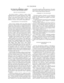
- FIG. 1 schematically illustrates a reactor 10 and associated equipment for the PECVD technique.
- At least one cathode 20 typically made of tungsten, is disposed in a cathode housing 30 .
- Anode plate 40 is disposed at one end of cathode housing 30 .
- at least a cathode housing is electrically floating.
- a voltage applied between cathode 20 and anode 40 generates an arc for plasma generation.
- a carrier gas such as argon, is fed through line 50 to the arc.
- a plasma is generated and exits a nozzle or orifice 70 at the center of anode 40 .
- a second reactant gas is optionally fed through supply line 80 to a point downstream from orifice 70 .
- Supply line 80 may also terminate with a perforated ring disposed within expanding plasma beam 84 for better mixing.
- Other reactant supply lines can be provided for different reactant species if desired. Radicals are generated from reactant gases, combined, carried to substrate 90 , and deposited thereon, which substrate is supported on substrate holder 100 .
- Substrate holder 100 is disposed opposite and at a distance from nozzle 70 and is movable relative to nozzle 70 by substrate-holder shaft 110 .
- Reactor 10 is kept under vacuum via vacuum connection 112 .
- the reactant gas can be deuterated benzene.
- a pre-etch of the substrate is employed.
- reactive species and energetic ions in the plasma are used to enhance adhesion of the coating or film to the substrate material.
- Pre-etching can serve several purposes simultaneously: removal of organic residues from the surface, removal of native oxide from the surface, and functionalization (formation of reactive sites) of the surface prior to the start of deposition.
- average substrate temperature is maintained at about 50° C. to about 130° C. throughout the process; more preferably, about 60° C. to about 90° C., and even more preferably about 70° C. to about 80° C.
- carrier gas flow is about 30 cc/s to about 200 cc/s. More preferably, about 60 cc/s to about 150 cc/s, and more preferably, about 75 cc/s about 125 cc/s.
- Pressure is maintained preferably at about 75 mTorr to about 250 mTorr, more preferably about 100 mTorr to about 200 mTorr, and even more preferably, about 125 mTorr to about 175 mTorr.
- Pre-etch input power can be maintained at about 50 W to about 150 W.
- the plasma input power can be maintained at about 10 W to 100 W. More preferably, about 25 W to about 75 W, and even more preferably, about 40 W to about 60 W. Deposition and etch times can be selected by the person of ordinary skill in the art to provide in a coating layer of desired thickness.
- deuterated hydrocarbon precursor e.g. CD 4 , deuterated alkanes, deuterated alkenes, and deuterated aromatics
- deuterated benzene C 6 D 6 was used for the a-C:D described herein.
- the a-C:D coatings applied to infrared optical elements provides the needed optical performance (e.g., adhesion, abrasion-resistance, antireflection) while enhancing transmission characteristics over previously used materials. Because of the improved transmittance, thicker coating designs can be utilized thereby increasing the applicability of these coatings for IR optical systems.
- Coating thicknesses in the 10 nm to 8 micron range can be used depending on the application.
- FIG. 2 shows that IR spectrum or both a-C:H and a-C:D are displayed showing the shift of absorptions in the 2900 cm ⁇ 1 range for the H-containing sample to higher energy in the a-C:D: sample.
Landscapes
- Chemical & Material Sciences (AREA)
- Physics & Mathematics (AREA)
- Optics & Photonics (AREA)
- General Physics & Mathematics (AREA)
- Chemical Kinetics & Catalysis (AREA)
- Materials Engineering (AREA)
- Mechanical Engineering (AREA)
- Metallurgy (AREA)
- Organic Chemistry (AREA)
- Engineering & Computer Science (AREA)
- General Chemical & Material Sciences (AREA)
- Inorganic Chemistry (AREA)
- Chemical Vapour Deposition (AREA)
- Surface Treatment Of Glass (AREA)
Abstract
Description
Claims (12)
Priority Applications (1)
| Application Number | Priority Date | Filing Date | Title |
|---|---|---|---|
| US11/034,606 US7294398B2 (en) | 2005-01-13 | 2005-01-13 | Deuterated amorphous carbon coating for infrared optics |
Applications Claiming Priority (1)
| Application Number | Priority Date | Filing Date | Title |
|---|---|---|---|
| US11/034,606 US7294398B2 (en) | 2005-01-13 | 2005-01-13 | Deuterated amorphous carbon coating for infrared optics |
Publications (2)
| Publication Number | Publication Date |
|---|---|
| US20060154073A1 US20060154073A1 (en) | 2006-07-13 |
| US7294398B2 true US7294398B2 (en) | 2007-11-13 |
Family
ID=36653597
Family Applications (1)
| Application Number | Title | Priority Date | Filing Date |
|---|---|---|---|
| US11/034,606 Expired - Lifetime US7294398B2 (en) | 2005-01-13 | 2005-01-13 | Deuterated amorphous carbon coating for infrared optics |
Country Status (1)
| Country | Link |
|---|---|
| US (1) | US7294398B2 (en) |
Families Citing this family (1)
| Publication number | Priority date | Publication date | Assignee | Title |
|---|---|---|---|---|
| JP2017518254A (en) * | 2014-04-18 | 2017-07-06 | ザ リサーチ ファウンデイション フォー ザ ステイト ユニバーシティー オブ ニューヨーク | Composite nanomaterials and micromaterials, their films, and their production methods and uses |
Citations (2)
| Publication number | Priority date | Publication date | Assignee | Title |
|---|---|---|---|---|
| US20040120685A1 (en) * | 2002-12-18 | 2004-06-24 | General Electric Company | Optical waveguide devices with deuterated amorphous carbon core structures |
| US6844070B2 (en) | 2002-08-30 | 2005-01-18 | Lockheed Martin Corporation | Low-temperature plasma deposited hydrogenated amorphous germanium carbon abrasion-resistant coatings |
-
2005
- 2005-01-13 US US11/034,606 patent/US7294398B2/en not_active Expired - Lifetime
Patent Citations (2)
| Publication number | Priority date | Publication date | Assignee | Title |
|---|---|---|---|---|
| US6844070B2 (en) | 2002-08-30 | 2005-01-18 | Lockheed Martin Corporation | Low-temperature plasma deposited hydrogenated amorphous germanium carbon abrasion-resistant coatings |
| US20040120685A1 (en) * | 2002-12-18 | 2004-06-24 | General Electric Company | Optical waveguide devices with deuterated amorphous carbon core structures |
Non-Patent Citations (1)
| Title |
|---|
| Fuchs et al "Hydrogen induced vibrational and electronic transitions in chemical vapor deposited diamond, identified by isotopic substitution" Appl. Phys. Lett 66 (2) Jan. 9, 1995. * |
Also Published As
| Publication number | Publication date |
|---|---|
| US20060154073A1 (en) | 2006-07-13 |
Similar Documents
| Publication | Publication Date | Title |
|---|---|---|
| KR960015223B1 (en) | Coating product and production method thereof | |
| EP0267679B1 (en) | Coated article and method of manufacturing the article | |
| US4737379A (en) | Plasma deposited coatings, and low temperature plasma method of making same | |
| US6086796A (en) | Diamond-like carbon over-coats for optical recording media devices and method thereof | |
| US6844070B2 (en) | Low-temperature plasma deposited hydrogenated amorphous germanium carbon abrasion-resistant coatings | |
| US10583632B2 (en) | Atomic oxygen-resistant, low drag coatings and materials | |
| US5067781A (en) | Optical elements and method of manufacture | |
| Pawlewicz et al. | Recent developments in reactively sputtered optical thin films | |
| US20160043247A1 (en) | Nitrogen-containing transparent conductive oxide cap layer composition | |
| JP2018513423A (en) | Coated optical object and method of manufacturing a coated optical object | |
| US5688608A (en) | High refractive-index IR transparent window with hard, durable and antireflective coating | |
| US7294398B2 (en) | Deuterated amorphous carbon coating for infrared optics | |
| US10705273B2 (en) | Multispectral interference coating with diamond-like carbon (DLC) film | |
| EP0429210B1 (en) | Optical elements and method of manufacture | |
| JP2015505900A (en) | Yttrium oxide coated optical element with improved mid-infrared performance | |
| Hennessy et al. | Ultrathin protective coatings by atomic layer engineering for far ultraviolet aluminum mirrors | |
| JP2001515542A (en) | Method for producing optically usable fluoride thin film and thin film thus produced | |
| Brierley et al. | Diamond coatings for large-area IR windows | |
| Raikar et al. | Surface characterization of SiC mirrors exposed to fast atomic oxygen | |
| JPH05129277A (en) | Multilayer reflection preventive film | |
| Lindsay et al. | Optical, composition, durability, and environmental properties of the microwave plasma-assisted sputter-deposited silicon nitride | |
| Sparks | Theoretical Studies of Materials for High-Power Infrared Coatings | |
| Clark et al. | New protective antireflecting coating for multispectral ZnS | |
| Iqbal et al. | Dual band nano structured anti reflection thin film coatings | |
| TWM604274U (en) | Diamond-like carbon composite film structure |
Legal Events
| Date | Code | Title | Description |
|---|---|---|---|
| AS | Assignment |
Owner name: LOCKHEED MARTIN CORPORATION, MARYLAND Free format text: ASSIGNMENT OF ASSIGNORS INTEREST;ASSIGNOR:GENERAL ELECTRIC COMPANY;REEL/FRAME:016176/0154 Effective date: 20041220 Owner name: GENERAL ELECTRIC COMPANY, NEW YORK Free format text: ASSIGNMENT OF ASSIGNORS INTEREST;ASSIGNORS:JOHSON, JAMES NEIL;BREITUNG, ERIC MICHAEL;REEL/FRAME:016176/0139;SIGNING DATES FROM 20041210 TO 20041220 |
|
| AS | Assignment |
Owner name: GENERAL ELECTRIC COMPANY, NEW YORK Free format text: CORRECTIVE COVERSHEET TO CORRECT TYPOGRAPHICAL ERROR OF INVENTOR'S LAST NAME PREVIOUSLY RECORDED ON REEL 016176, FRAME 0139.;ASSIGNORS:JOHNSON, JAMES NEIL;BREITUNG, ERIC MICHAEL;REEL/FRAME:016631/0852;SIGNING DATES FROM 20041210 TO 20041220 |
|
| STCF | Information on status: patent grant |
Free format text: PATENTED CASE |
|
| FPAY | Fee payment |
Year of fee payment: 4 |
|
| FPAY | Fee payment |
Year of fee payment: 8 |
|
| MAFP | Maintenance fee payment |
Free format text: PAYMENT OF MAINTENANCE FEE, 12TH YEAR, LARGE ENTITY (ORIGINAL EVENT CODE: M1553); ENTITY STATUS OF PATENT OWNER: LARGE ENTITY Year of fee payment: 12 |