US7286433B2 - Method for activating a plurality of word lines in a refresh cycle, and electronic memory device - Google Patents
Method for activating a plurality of word lines in a refresh cycle, and electronic memory device Download PDFInfo
- Publication number
- US7286433B2 US7286433B2 US11/294,055 US29405505A US7286433B2 US 7286433 B2 US7286433 B2 US 7286433B2 US 29405505 A US29405505 A US 29405505A US 7286433 B2 US7286433 B2 US 7286433B2
- Authority
- US
- United States
- Prior art keywords
- memory
- word lines
- cell array
- memory cell
- memory cells
- Prior art date
- Legal status (The legal status is an assumption and is not a legal conclusion. Google has not performed a legal analysis and makes no representation as to the accuracy of the status listed.)
- Expired - Fee Related, expires
Links
- 238000000034 method Methods 0.000 title claims description 21
- 230000003213 activating effect Effects 0.000 title 1
- 230000015654 memory Effects 0.000 claims abstract description 158
- 230000004913 activation Effects 0.000 claims abstract description 12
- 238000005516 engineering process Methods 0.000 description 3
- 230000014759 maintenance of location Effects 0.000 description 3
- 238000004519 manufacturing process Methods 0.000 description 3
- 230000008569 process Effects 0.000 description 3
- 230000008901 benefit Effects 0.000 description 2
- 238000011161 development Methods 0.000 description 2
- 238000012986 modification Methods 0.000 description 2
- 230000004048 modification Effects 0.000 description 2
- 102000001690 Factor VIII Human genes 0.000 description 1
- 108010054218 Factor VIII Proteins 0.000 description 1
- 239000003990 capacitor Substances 0.000 description 1
- 230000001419 dependent effect Effects 0.000 description 1
- 238000013461 design Methods 0.000 description 1
- 230000006870 function Effects 0.000 description 1
- 230000006872 improvement Effects 0.000 description 1
- 238000012423 maintenance Methods 0.000 description 1
- 238000005457 optimization Methods 0.000 description 1
- 238000012545 processing Methods 0.000 description 1
- 230000009467 reduction Effects 0.000 description 1
Images


Classifications
-
- G—PHYSICS
- G11—INFORMATION STORAGE
- G11C—STATIC STORES
- G11C11/00—Digital stores characterised by the use of particular electric or magnetic storage elements; Storage elements therefor
- G11C11/21—Digital stores characterised by the use of particular electric or magnetic storage elements; Storage elements therefor using electric elements
- G11C11/34—Digital stores characterised by the use of particular electric or magnetic storage elements; Storage elements therefor using electric elements using semiconductor devices
- G11C11/40—Digital stores characterised by the use of particular electric or magnetic storage elements; Storage elements therefor using electric elements using semiconductor devices using transistors
- G11C11/401—Digital stores characterised by the use of particular electric or magnetic storage elements; Storage elements therefor using electric elements using semiconductor devices using transistors forming cells needing refreshing or charge regeneration, i.e. dynamic cells
- G11C11/406—Management or control of the refreshing or charge-regeneration cycles
- G11C11/40618—Refresh operations over multiple banks or interleaving
-
- G—PHYSICS
- G11—INFORMATION STORAGE
- G11C—STATIC STORES
- G11C11/00—Digital stores characterised by the use of particular electric or magnetic storage elements; Storage elements therefor
- G11C11/21—Digital stores characterised by the use of particular electric or magnetic storage elements; Storage elements therefor using electric elements
- G11C11/34—Digital stores characterised by the use of particular electric or magnetic storage elements; Storage elements therefor using electric elements using semiconductor devices
- G11C11/40—Digital stores characterised by the use of particular electric or magnetic storage elements; Storage elements therefor using electric elements using semiconductor devices using transistors
- G11C11/401—Digital stores characterised by the use of particular electric or magnetic storage elements; Storage elements therefor using electric elements using semiconductor devices using transistors forming cells needing refreshing or charge regeneration, i.e. dynamic cells
- G11C11/406—Management or control of the refreshing or charge-regeneration cycles
Definitions
- the present invention relates to electronic memory devices such as DRAMs (Dynamic Random Access Memories, dynamic read/write memories), and relates particularly to a method and apparatus for refreshing information stored in memory cells in a memory cell array.
- DRAMs Dynamic Random Access Memories, dynamic read/write memories
- the present invention relates specifically to an electronic memory device for storing data having a memory cell array, for example arranged in memory banks, which has memory cells and having word lines and bit lines for addressing/reading the memory cells in the memory cell array, with information stored in the memory cells in the memory cell array being refreshed by applying a predetermined activation potential at a predetermined refresh rate to the word lines.
- Retention problems i.e. problems in retaining the stored information or the stored electrical charge
- future production technologies such as 90-nanometer technology or 70-nanometer technology are used.
- the drawback arises that the memory cells formed from trench capacitors, for example, need to be produced in ever narrower and deeper form, which gives rise to leakage paths which result in a reduction in the electrical charge stored in the memory cells.
- an electronic memory device for storing data essentially, comprising: a memory cell array which is arranged in memory banks and which has memory cells; and word lines and bit lines for addressing the memory cells in the memory cell array, where information stored in the memory cells in the memory cell array can be refreshed by applying a predetermined activation potential at a predetermined refresh rate to the word lines, with all word lines in a memory bank which do not have a common bit line being able to be activated in a refresh mode.
- a) information in the form of electrical charge is stored in memory cells in a memory cell array which has memory banks;
- the memory cells in the memory cell array are addressed using word lines and bit lines, where information stored in the memory cells in the memory cell array is refreshed by applying a predetermined activation potential at a predetermined refresh rate to the word lines, with all word lines in a memory bank which do not have a common bit line being able to be activated in a refresh mode.
- a fundamental concept of the invention involves an increased number of word lines (in comparison with the prior art) in a memory bank which forms part of an electronic memory apparatus being activated simultaneously in order to perform a refresh procedure.
- an increase in the number of activated word lines improves a refresh operation. It is also expedient that when the number of activatable word lines is increased the refresh rate for a refresh process can be reduced, i.e. that a time between individual refresh cycles can be increased.
- DRAMs Dynamic Random Access Memories, dynamic read/write memories
- the inventive electronic memory device may be a 256-Mb DRAM chip with four memory banks.
- the four memory banks are of the same size, i.e. they have a memory depth of 64 Mb (megabits).
- the memory banks may be provided from memory blocks which can be activated using a respective particular number of associated word lines.
- the refresh rate for a refresh process for the memory cells arranged in the memory apparatus may be 64 ms.
- Each of the memory blocks in the memory apparatus may have an associated separate sense amplifier block.
- Information stored in the memory cells in the memory cell array may be refreshed periodically. This means that the inventive electronic memory device for storing data allows a safe refresh mode to be provided even when the structures of the individual memory cells are reduced in size.
- FIG. 1 is a memory cell array with memory cells arranged in memory banks in accordance with a preferred exemplary embodiment of the present invention.
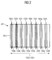
- FIG. 2 is an enlarged detail of one of the memory cell array's memory banks of FIG. 1 .
- FIG. 1 shows a memory apparatus which essentially comprises a memory cell array 100 .
- Individual memory cells are shown schematically by the reference symbols 100 a - 100 m .
- the memory cell array is split into four memory banks 101 a , 101 b , 101 c and 101 d.
- the memory cell array described has a total memory depth of 256 megabits (Mb), for example. If the memory depth is split evenly, each individual memory bank 101 a - 101 d thus has a memory depth of 64 Mb.
- the individual memory cells are addressed/read using word lines 102 a - 102 n and bit lines (not shown). It should be pointed out that all four memory banks 101 a - 101 d are addressed using such word lines 102 a - 102 n , even though FIG. 1 illustrates such a word line structure only for the memory bank 101 c .
- the memory bank 101 c (like the other memory banks 101 a , 101 b and 101 d too) is divided into individual memory blocks, which are denoted by the reference symbols 103 a , . . . , 103 k with reference to the memory bank 101 c.
- the memory blocks 103 a - 103 k each have a memory depth of 4 megabits (Mb). Each 4-Mb memory block 103 a - 103 k is addressed by separately associated word lines. Each of the memory banks 101 a - 101 d thus has a number of 16 4-Mb memory blocks 103 a - 103 k . Preferably, each of the memory blocks 103 a - 103 k has an associated separate sense amplifier block. In line with the inventive method for storing data, a plurality of word lines now become activatable for a memory bank without there being any reciprocal influencing.
- FIG. 1 thus illustrates 16 individual memory blocks using the digits 1 to 16.
- a number of 1024 chip selection lines CSL is provided for each memory bank in this case.
- only the memory blocks identified by a dashed area are activated simultaneously by the word line for the purpose of a refresh operation.
- it is now possible to activate more than two word lines per memory bank (word lines which belong to more than one address).
- FIG. 2 shows an enlarged detail of one of the memory banks 101 a - 101 d which are shown in FIG. 1 .
- the memory bank 101 c has been selected, with all the memory banks 101 a - 101 d based on the preferred exemplary embodiment of the invention being of identical design.
- eight memory blocks 103 a - 103 h are shown in the memory bank 101 c illustrated in FIG. 2 , these being able to be addressed or activated using appropriately associated word lines 102 a - 102 h in order to be able to perform a refresh cycle (refresh process).
- the memory blocks 103 b and 103 f shown by a shaded area in FIG. 2 are normally addressed simultaneously during a refresh cycle.
- it is now possible to address more than two memory blocks 103 b , 103 f per memory bank 101 c i.e. in the present case of a 64-Mb memory bank 101 c a number of up to 16 memory blocks 103 a - 103 h which each have a memory depth of 4 megabits (Mb), i.e. the inventive method for storing data allows an increase in the refresh rate for the 64-Mb memory bank by a maximum of the factor 8.
- FIG. 2 shows the activation of eight memory blocks 103 a - 103 h using appropriately associated word lines 102 a - 102 h by way of example.
- inventive method for storing data can also be applied in corresponding fashion to memory banks with a greater or lesser memory depth than 64 Mb (megabits).
- a crucial factor for the application of the inventive method in this context is that information stored in the memory cells 100 a - 100 m in the memory cell array 100 is refreshed by applying a predetermined activation potential 201 (shown only for the first word line 102 a in FIG. 2 ) at a predetermined refresh rate t to all word lines 102 a - 102 n , with all word lines 102 a - 102 n in a memory bank 101 a - 101 d which do not have a common bit line being activated in a refresh mode.
Landscapes
- Engineering & Computer Science (AREA)
- Microelectronics & Electronic Packaging (AREA)
- Computer Hardware Design (AREA)
- Dram (AREA)
Abstract
Description
64 ms/8k=t refresh=8 μs (1)
To implement the inventive method for storing data, it is possible to ignore certain address bits. In the case of a 256-Mb memory cell array (memory chip D11), the most significant address bits (RA12:10) define that memory block among the 4-Mb memory blocks 103 a-103 k in which an activation operation needs to be performed.
Claims (9)
Applications Claiming Priority (2)
| Application Number | Priority Date | Filing Date | Title |
|---|---|---|---|
| DE102004059671A DE102004059671B4 (en) | 2004-12-10 | 2004-12-10 | Method for activating word lines in a refresh cycle and electronic memory device for carrying out the method |
| DE102004059671.9-55 | 2004-12-10 |
Publications (2)
| Publication Number | Publication Date |
|---|---|
| US20060126414A1 US20060126414A1 (en) | 2006-06-15 |
| US7286433B2 true US7286433B2 (en) | 2007-10-23 |
Family
ID=36500209
Family Applications (1)
| Application Number | Title | Priority Date | Filing Date |
|---|---|---|---|
| US11/294,055 Expired - Fee Related US7286433B2 (en) | 2004-12-10 | 2005-12-05 | Method for activating a plurality of word lines in a refresh cycle, and electronic memory device |
Country Status (2)
| Country | Link |
|---|---|
| US (1) | US7286433B2 (en) |
| DE (1) | DE102004059671B4 (en) |
Cited By (1)
| Publication number | Priority date | Publication date | Assignee | Title |
|---|---|---|---|---|
| US9082504B2 (en) | 2012-07-12 | 2015-07-14 | Samsung Electronics Co., Ltd. | Semiconductor memory device storing refresh period information and operating method thereof |
Citations (6)
| Publication number | Priority date | Publication date | Assignee | Title |
|---|---|---|---|---|
| US5715206A (en) * | 1995-08-24 | 1998-02-03 | Samsung Electronics Co., Ltd. | Dynamic random access memory having sequential word line refresh |
| US6067261A (en) * | 1998-08-03 | 2000-05-23 | International Business Machines Corporation | Timing of wordline activation for DC burn-in of a DRAM with the self-refresh |
| US6469947B2 (en) * | 1999-06-29 | 2002-10-22 | Hyundai Electronics Co., Ltd. | Semiconductor memory device having regions with independent word lines alternately selected for refresh operation |
| JP3409274B2 (en) | 1997-10-07 | 2003-05-26 | 沖電気工業株式会社 | Optical multiplexing circuit and optical demultiplexing circuit |
| DE10317364A1 (en) | 2003-04-15 | 2004-11-18 | Infineon Technologies Ag | Integrated dynamic memory with control circuit for controlling a refresh operation of memory cells |
| US6842392B2 (en) * | 2000-10-27 | 2005-01-11 | Seiko Epson Corporation | Activation of word lines in semiconductor memory device |
Family Cites Families (1)
| Publication number | Priority date | Publication date | Assignee | Title |
|---|---|---|---|---|
| JP2762589B2 (en) * | 1989-07-21 | 1998-06-04 | 日本電気株式会社 | Semiconductor memory circuit |
-
2004
- 2004-12-10 DE DE102004059671A patent/DE102004059671B4/en not_active Expired - Fee Related
-
2005
- 2005-12-05 US US11/294,055 patent/US7286433B2/en not_active Expired - Fee Related
Patent Citations (7)
| Publication number | Priority date | Publication date | Assignee | Title |
|---|---|---|---|---|
| US5715206A (en) * | 1995-08-24 | 1998-02-03 | Samsung Electronics Co., Ltd. | Dynamic random access memory having sequential word line refresh |
| JP3409274B2 (en) | 1997-10-07 | 2003-05-26 | 沖電気工業株式会社 | Optical multiplexing circuit and optical demultiplexing circuit |
| US6067261A (en) * | 1998-08-03 | 2000-05-23 | International Business Machines Corporation | Timing of wordline activation for DC burn-in of a DRAM with the self-refresh |
| US6469947B2 (en) * | 1999-06-29 | 2002-10-22 | Hyundai Electronics Co., Ltd. | Semiconductor memory device having regions with independent word lines alternately selected for refresh operation |
| US6842392B2 (en) * | 2000-10-27 | 2005-01-11 | Seiko Epson Corporation | Activation of word lines in semiconductor memory device |
| DE10317364A1 (en) | 2003-04-15 | 2004-11-18 | Infineon Technologies Ag | Integrated dynamic memory with control circuit for controlling a refresh operation of memory cells |
| US6940775B2 (en) | 2003-04-15 | 2005-09-06 | Infineon Technologies, Ag | Integrated dynamic memory having a control circuit for controlling a refresh mode for memory cells |
Non-Patent Citations (1)
| Title |
|---|
| German Office Action dated Oct. 12, 2005. |
Cited By (1)
| Publication number | Priority date | Publication date | Assignee | Title |
|---|---|---|---|---|
| US9082504B2 (en) | 2012-07-12 | 2015-07-14 | Samsung Electronics Co., Ltd. | Semiconductor memory device storing refresh period information and operating method thereof |
Also Published As
| Publication number | Publication date |
|---|---|
| DE102004059671B4 (en) | 2007-03-22 |
| US20060126414A1 (en) | 2006-06-15 |
| DE102004059671A1 (en) | 2006-06-14 |
Similar Documents
| Publication | Publication Date | Title |
|---|---|---|
| US12002501B2 (en) | Apparatuses and methods for distributed targeted refresh operations | |
| US11615831B2 (en) | Apparatuses and methods for memory mat refresh sequencing | |
| US11538515B2 (en) | DRAM memory | |
| KR100621619B1 (en) | Semiconductor Memory Device Performing Refresh Operation | |
| US9412432B2 (en) | Semiconductor storage device and system provided with same | |
| CN114077816A (en) | Refresh the logic circuit layout | |
| KR102501651B1 (en) | Refresh control device | |
| CN113168861A (en) | Semiconductor device for performing row hammer refresh operation | |
| US7755967B2 (en) | Memory device refresh method and apparatus | |
| US10740188B2 (en) | Volatile memory device and method for efficient bulk data movement, backup operation in the volatile memory device | |
| US11763870B2 (en) | Apparatuses, systems, and methods for ferroelectric memory cell operations | |
| US20030214832A1 (en) | Semiconductor memory device switchable to twin memory cell configuration | |
| US10878879B2 (en) | Refresh control method for memory system to perform refresh action on all memory banks of the memory system within refresh window | |
| KR102457630B1 (en) | Semiconductor device and memory module including the same | |
| US7286433B2 (en) | Method for activating a plurality of word lines in a refresh cycle, and electronic memory device | |
| US10290342B2 (en) | Methods and apparatus for memory programming | |
| US5663916A (en) | Apparatus and method for minimizing DRAM recharge time | |
| US7492662B2 (en) | Structure and method of implementing power savings during addressing of DRAM architectures | |
| US6999369B2 (en) | Circuit and method for refreshing memory cells of a dynamic memory | |
| US12176018B2 (en) | Semiconductor memory, method for refreshing, method for controlling and electronic device | |
| KR100482380B1 (en) | SRAM compatable memory having memory banks capable of indepedently writing access and Operating Method thereof | |
| US7277977B2 (en) | DRAM for high-speed data access | |
| US5764582A (en) | Apparatus and method of refreshing a dynamic random access memory | |
| US7797511B2 (en) | Memory refresh system and method | |
| WO2004027781A1 (en) | Refreshing of multi-port memory in integrated circuits |
Legal Events
| Date | Code | Title | Description |
|---|---|---|---|
| AS | Assignment |
Owner name: INFINEON TECHNOLOGIES AG, GERMANY Free format text: ASSIGNMENT OF ASSIGNORS INTEREST;ASSIGNORS:ANTRETTER, RICHARD;MOSER, MANFRED;REEL/FRAME:017216/0218;SIGNING DATES FROM 20051214 TO 20051215 |
|
| STCF | Information on status: patent grant |
Free format text: PATENTED CASE |
|
| FEPP | Fee payment procedure |
Free format text: PAYOR NUMBER ASSIGNED (ORIGINAL EVENT CODE: ASPN); ENTITY STATUS OF PATENT OWNER: LARGE ENTITY |
|
| AS | Assignment |
Owner name: QIMONDA AG, GERMANY Free format text: ASSIGNMENT OF ASSIGNORS INTEREST;ASSIGNOR:INFINEON TECHNOLOGIES AG;REEL/FRAME:023806/0001 Effective date: 20060425 Owner name: QIMONDA AG,GERMANY Free format text: ASSIGNMENT OF ASSIGNORS INTEREST;ASSIGNOR:INFINEON TECHNOLOGIES AG;REEL/FRAME:023806/0001 Effective date: 20060425 |
|
| FPAY | Fee payment |
Year of fee payment: 4 |
|
| FPAY | Fee payment |
Year of fee payment: 8 |
|
| AS | Assignment |
Owner name: INFINEON TECHNOLOGIES AG, GERMANY Free format text: ASSIGNMENT OF ASSIGNORS INTEREST;ASSIGNOR:QIMONDA AG;REEL/FRAME:035623/0001 Effective date: 20141009 |
|
| AS | Assignment |
Owner name: POLARIS INNOVATIONS LIMITED, IRELAND Free format text: ASSIGNMENT OF ASSIGNORS INTEREST;ASSIGNOR:INFINEON TECHNOLOGIES AG;REEL/FRAME:036908/0923 Effective date: 20150708 |
|
| FEPP | Fee payment procedure |
Free format text: MAINTENANCE FEE REMINDER MAILED (ORIGINAL EVENT CODE: REM.); ENTITY STATUS OF PATENT OWNER: LARGE ENTITY |
|
| LAPS | Lapse for failure to pay maintenance fees |
Free format text: PATENT EXPIRED FOR FAILURE TO PAY MAINTENANCE FEES (ORIGINAL EVENT CODE: EXP.); ENTITY STATUS OF PATENT OWNER: LARGE ENTITY |
|
| STCH | Information on status: patent discontinuation |
Free format text: PATENT EXPIRED DUE TO NONPAYMENT OF MAINTENANCE FEES UNDER 37 CFR 1.362 |
|
| FP | Lapsed due to failure to pay maintenance fee |
Effective date: 20191023 |