US7285915B2 - Electron gun for producing incident and secondary electrons - Google Patents
Electron gun for producing incident and secondary electrons Download PDFInfo
- Publication number
- US7285915B2 US7285915B2 US09/995,077 US99507701A US7285915B2 US 7285915 B2 US7285915 B2 US 7285915B2 US 99507701 A US99507701 A US 99507701A US 7285915 B2 US7285915 B2 US 7285915B2
- Authority
- US
- United States
- Prior art keywords
- electrons
- cavity
- electron
- area
- gun
- Prior art date
- Legal status (The legal status is an assumption and is not a legal conclusion. Google has not performed a legal analysis and makes no representation as to the accuracy of the status listed.)
- Expired - Fee Related, expires
Links
Images


Classifications
-
- H—ELECTRICITY
- H01—ELECTRIC ELEMENTS
- H01J—ELECTRIC DISCHARGE TUBES OR DISCHARGE LAMPS
- H01J23/00—Details of transit-time tubes of the types covered by group H01J25/00
- H01J23/02—Electrodes; Magnetic control means; Screens
- H01J23/06—Electron or ion guns
-
- H—ELECTRICITY
- H01—ELECTRIC ELEMENTS
- H01J—ELECTRIC DISCHARGE TUBES OR DISCHARGE LAMPS
- H01J3/00—Details of electron-optical or ion-optical arrangements common to two or more basic types of discharge tubes or lamps
- H01J3/02—Electron guns
- H01J3/023—Electron guns using electron multiplication
Definitions
- the present invention is related to electron guns. More specifically, the present invention is related to an electron gun that uses an RF cavity subjected to an oscillating electric field.
- High-current pulses are widely used in injector systems for electron accelerators, both for industrial linacs as well as high-energy accelerators for linear colliders.
- Short-duration pulses are also used for microwave generation, in klystrons and related devices, for research on advanced methods of particle acceleration, and for injectors used for free-electron-laser (FEL) drivers.
- FEL free-electron-laser
- the difficulty of generating very high-current pulses of short duration can be illustrated by examination of a modern linac injector system.
- a good example is the system designed and built for the Boeing 120 MeV, 1300 MHz linac, which in turn is used as a FEL driver [J. L. Adamski et al., IEEE Trans. Nucl. Sci. NS-32, 3397 (1985); T. F. Godlove and P. Sprangle, Particle Accelerators 34, 169 (1990)].
- the Boeing system uses: (a) a gridded, 100 kV electron gun pulsed with a 3-nanosecond pulse; (b) two low-power prebunchers, the first operating at 108 MHz and the second at 433 MHz; and (c) a high-power, tapered-velocity buncher which accelerates the beam bunches up to 2 MeV.
- the design relies on extensive calculations with computer codes such as EGUN and PARMELA. A carefully tapered, axial magnetic field is applied which starts from zero at the cathode and rises to about 500 Gauss.
- Boeing obtains a peak current up to about 400 A in pulses of 15 to 20 ps duration, with good emittance.
- the bunching process yields a peak current which is two orders of magnitude larger than the electron gun current.
- Space charge forces, which cause the beam to expand both radially and axially, are minimized by using a strong electric field in the high-power buncher, and finally are balanced by forces due to the axial magnetic field.
- the performance achieved by Boeing appears to be at or near the limit of this type of injector.
- Micro-pulses or bunches are produced by resonantly amplifying a current of secondary electrons in an rf cavity. Bunching occurs rapidly and is followed by saturation of the current density within ten rf periods.
- the “bunching” process is not the conventional method of compressing a long beam into a short one, but results by selecting particles that are in phase with the rf electric field, i.e., resonant.
- One wall of the cavity is highly transparent to electrons but opaque to the input rf field. The transparent wall allows for the transmission of the energetic electron bunches and serves as the cathode of a high-voltage injector.
- FIG. 1 shows a perspective view of the micropulse gun emitting electron-bunches in an annular geometry.
- This micro-pulse electron gun should provide a high peak power, multi-kiloampere, picosecond-long electron source which is suitable for many applications. Of particular interest are: high energy picosecond electron injectors for linear colliders, free electron lasers and high harmonic rf generators for linear colliders, or super-power nanosecond radar.
- the present invention pertains to an electron gun.
- the electron gun comprises an RF cavity having a first side with an emitting surface and a second side with a transmitting and emitting section.
- the gun is also comprised of a mechanism for producing an oscillating force which encompasses the emitting surface and the section so electrons are directed between the emitting surface and the section to contact the emitting surface and generate additional electrons and to contact the section to generate additional electrons or escape the cavity through the section.
- the section preferably isolates the cavity from external forces outside and adjacent the cavity.
- the section preferably includes a transmitting and emitting screen.
- the screen can be of an annular shape, or of a circular shape, or of a rhombohedron shape.
- the mechanism preferably includes a mechanism for producing an oscillating electric field that provides the force and which has a radial component that prevents the electrons from straying out of the region between the screen and the emitting surface. Additionally, the gun includes a mechanism for producing a magnetic field to force the electrons between the screen and the emitting surface.
- the present invention pertains to a method for producing electrons.
- the method comprises the steps of moving at least a first electron in a first direction. Next there is the step of striking a first area with the first electron. Then there is the step of producing additional electrons at the first area due to the first electron. Next there is the step of moving electrons from the first area to a second area and transmitting electrons through the second area and creating more electrons due to electrons from the first area striking the second area. These newly created electrons from the second area then strike the first area, creating even more electrons in a recursive, repeating manner between the first and second areas.
- FIG. 1 is a perspective view of the micropulse gun for a hollow beam in the TM 020 mode. The inner conductor is not shown.
- FIG. 2 is a schematic of rf gun operating in TM 020 mode.
- FIG. 3 is a schematic of micropulse gun for solid beam (TM 010 ) mode.
- a coaxial feed is used for rf input (not shown).
- FIG. 4 is a secondary electron emission yield curve for GaP and MgO.
- FIG. 5 is a schematic drawing of model used in theoretical analysis.
- FIG. 6 is a steady-state current density and bunch length vs. rf field, all parameters are normalized.
- FIG. 14 is a micro-pulse width (as a fraction of the half-cycle) vs. rf cycle number near the output grid.
- the full beam pulse width decreases with time, and reaches a minimum at the fourth rf cycle. After saturation there is a slight increase in pulse-width due to space-charge effects.
- FIG. 15 is a longitudinal electric field in kv/cm as measured by a probe near the exit grid for the 6.4 GHz, 105 kV simulation.
- FIG. 16 is a plot of the current density in kA/cm 2 [solid line] and the longitudinal electric field [dashed line] for the 6.4 GHz, 105 kV simulation.
- FIG. 17 is a resonant Tuning Curve (both simulation and theory) showing the tolerance of the micropulse electron gun.
- FIG. 19 is a side view of a cylindrical symmetric coaxial transmission line and cavity. An rf wave is launched at the left end of the coaxial line.
- FIG. 20 is resulting voltages for a TM 010 cavity at 1.275 GHz (9 cm radius) with a one cm cavity gap and one cm coaxial gap. (top) voltage measured at entrance of coax, and (bottom) voltage measured at cavity center.
- FIG. 21 is an electric field from a coaxially fed cavity (TM 010 mode) showing simulation values (open circles) and theoretical curve for an ideal closed cavity.
- FIG. 23 is an electric field from a coaxially fed cavity (TM 020 mode) showing simulation values (open circles) and theoretical curve for an ideal closed cavity.
- FIG. 24 is an axial electric field vs. radius from a coaxially fed cavity (TM 020 mode (simulation) with inner conductor at first zero of the mode. The first peak has clearly been eliminated. Frequency 1.275 GHz and one cm gap.
- FIG. 25 is an axial electric field as a function of radius loaded down by a 40 amp/cm 2 , 25 ps pulse, and one cm diameter electron beam. The curve is inverted compared to the plot of FIG. 24 . However, the depression at R ⁇ 14 cm due to space charge is clearly seen.
- FIG. 27 is a configuration space and phase space for a solid beam from the simulations. This shows the emittance growth up to the first grid, from the first grid, and from the second grid.
- FIG. 28 is a normalized emmitance and transmission versus number of grid wires with an ac voltage applied to the cavity.
- Grid wire radius is 0.09615 mm.
- FIG. 29 is an expansion of micro-pulse from space charge during acceleration, neglecting energy spread.
- the acceleration field is 20 MV/m and the axial space charge electric field is 2.9 MV/m (corresponding to about 100 nC/cm 3 ).
- the initial pulse width is 5 ps at an initial energy of 50 kev.
- FIG. 30 is a schematic drawing of a set of electrode shapes for a high-power diode using the modified formulas to the usual Pierce shapes as discussed below.
- FIG. 31 is a plot of electrode shapes for a non-space-charge-limited 0.5 MeV diode.
- the modified shapes [solid lines] and the classical Pierce shapes [broken lines] are shown for comparison.
- FIG. 33 is an emission area for a solid beam vs. frequency for different energy spreads (top) 1%-4% energy spread; (bottom) 10%-30% energy spread.
- FIG. 35 is a beam current (solid beam) vs. frequency for different energy spreads and a gap of 1.0 cm.
- FIG. 36 is a charge per pulse f or a solid beam vs. energy spread.
- FIG. 37 is an emission area vs. frequency for different energy spreads. Hollow beam.
- FIG. 40 is a pulse charge vs. energy for hollow beam.
- FIG. 45 is a magnetron feeding energy into the rf cavity. For simplicity a constant, low impedance, coaxial feed line is assumed. Voltage step-up occurs in the rf cavity.
- the section 20 preferably isolates the cavity 12 from external forces outside and adjacent the cavity 12 .
- the section 20 preferably includes a transmitting and emitting screen 24 .
- the screen 24 can be of an annular shape, or of a circular shape, or of a rhombohedron shape.
- the mechanism 22 preferably includes a mechanism 26 for producing an oscillating electric field that provides the force and which has a radial component that prevents the electrons 11 from straying out of the region between the screen 24 and the emitting surface 16 . Additionally, the gun 10 includes a mechanism 28 for producing a magnetic field to force the electrons 11 between the screen 24 and the emitting surface 16 .
- the present invention pertains to a method for producing electrons 11 .
- the method comprises the steps of moving at least a first electron 11 in a first direction. Next there is the step of striking a first area with the first electron 11 . Then there is the step of producing additional electrons 11 at the first area due to the first electron 11 . Next there is the step of moving electrons from the first area to a second area and transmitting electrons 21 through the second area and creating more electrons 11 due to electrons from the first area striking the second area. This process is repeated until the device is shut off by removing the rf power source.
- FIG. 2 A schematic of one embodiment of the proposed device is given in FIG. 2 .
- the rf power is fed into the cavity by a low impedance coaxial transmission line connected to the perimeter of the cavity.
- rf power may be fed into the cavity by the conventional method of side coupling using a tapered waveguide.
- the appropriate mode is then set up (in this case the TM 020 mode).
- An annular electron pulse is generated by secondary emission at the second peak of the electric field in the cavity operating in a TM 020 mode.
- the first peak is eliminated by placing an inner conducting cylinder at the first zero of the TM 020 mode.
- the pulse rapidly bunches and reaches a saturated state within several rf periods. This rapid bunching and saturation is due to a combination of the space charge field and the resonant rf field condition.
- the right wall of the cavity in FIG. 2 (also see detail) is constructed with a transmitting annular shaped double screen (grid) which allows for the transmission of a high current density hollow electron pulse.
- the radial wires maintain a path for the rf current.
- the double screen provides a means to isolate the accelerating and rf fields thus preventing the accelerating field from pulling out electrons that are not resonant with the rf field.
- the second grid (to the right) is electrically isolated from the first grid and can be dc biased ( ⁇ 100 volts) to create a barrier for low energy electrons.
- the emittance in the micro-pulse gun (MPG) is lower than would be expected for a dc gun.
- MPG micro-pulse gun
- the main point is that the resonant particles are loaded into the wave at low phase angles and when they reach the opposite electrode or grid, they experience a reduced transverse kick from the grid wires.
- radial expansion is controlled by an axial magnetic field.
- the short-pulse, high-current electron pulse leaves the cavity with high kinetic energy.
- the pulse is then accelerated to much higher energy by either electrostatic, inductive or rf means.
- the application for the above hollow beam configuration is primarily suited to high harmonic microwave production.
- An alternative configuration which produces a solid beam is the TM 010 mode. This configuration will be more suitable for injector applications.
- FIG. 3 In FIG. 3 is shown an rf cavity operating in a TM 010 mode. Now assume at one of the electrode walls (the screen or grid) of the cavity there is a single electron at rest near the axis. This electron is accelerated across the cavity and strikes the surface S. A number ⁇ 1 of secondary electrons are emitted off this electrode. Provided the average transit time of an electron in the cavity is one-half the rf period, and that the secondary electrons are in the proper phase with the rf field, these electrons will be accelerated towards the screen. If ⁇ 1 is the secondary electron yield per primary electron, then upon reaching the screen, ⁇ 1 T electrons will be transmitted where T is the transmission factor of the screen. The number of electrons which are not transmitted is then ⁇ 1 (1 ⁇ T).
- the seed current density can be created by any of several sources including cosmic rays, a thermionic source, ultraviolet light, field emission, a spark, nuclear disintegration, etc.
- High current density secondary emission (>1500 A/cm 2 ) has been achieved with doped silicon that is prepared with cesium [G. G. P. van Gorkom and A. M. E. Hoeberechts, J. Vac. Sci. Tech. B, 4, 108(1986)].
- the emitting surface is easily contaminated by exposure to O 2 .
- GaP+Cs can be used as the secondary emitter for the proposed device at high current densities since it is more robust and not sensitive to O 2 .
- Several photomultipliers (RCA C31024, RCA C31050 and RCA 8850 are built with GaP dynodes.
- the current density limit for GaP is not known as yet, but it is expected to be comparable to the doped silicon since high yield emitters are also high current density emitters.
- GaAs is another candidate emitter but is sensitive to O 2 .
- MgO is a good candidate for low current densities and would have to be applied in a thin layer in order to avoid charge buildup.
- Another very robust emitter material is diamond film [M. W. Geiss, N. N. Efremow, J. D. Woodhouse, M. D. McAleese, M. Marchywka, D. G. Socker, and J. F. Hochedez, “Diamond Cold Cathode”, IEEE Electron Device Letters 12, 8 (1991)].
- Single crystal alumina (sapphire) or polycrystalline alumina are also excellent robust emitters. Thin layers need to be applied to avoid charge buildup.
- V 0 m ⁇ ⁇ ⁇ 2 ⁇ d 2 e ⁇ [ 1 - v 0 ⁇ ⁇ / ⁇ ⁇ ⁇ d ] / ⁇ ( 8 )
- ⁇ has a maximum value which gives rise to a minimum resonance condition. At the minimum resonance condition the phase angle ⁇ is about 32.5°.
- the resonant voltage V 0 can be determined from the above equation to be
- the probability for a secondary electron to be emitted between the angles ⁇ and ⁇ can be derived from the cos 2 ⁇ law as
- FIG. 5 The axial electron bunch length 11 or charge slab thickness is ⁇ , the axial gap spacing between the parallel plates or electrodes 14 is d, and the beam density is n.
- the equations of motion for electrons “attached” to the front (“f”) (label 3 in FIG. 5 ) and back (“b”) (label 1 in FIG. 5 of the charge slab are evaluated.
- An electron in the center of the bunch (label 2 in FIG. 5 ) would have no space charge and travel according to Eq. (5).
- the equations of motion are
- J J 0 ⁇ s ⁇ ⁇ 2 ⁇ ⁇ 0 ⁇ cos ⁇ ⁇ ⁇ f + ⁇ ⁇ ⁇ ⁇ s ( ⁇ / d ) FWHM ⁇ ⁇
- J 0 ⁇ 0 ⁇ m e ⁇ ⁇ 3 ⁇ d
- FMTSEC FMT-developed special secondary emission code
- FMTSEC is defined as a particle-in-cell computer simulation code capable of handling secondary emission. It is a completely self-consistent two-dimensional relativistic particle-in-cell code which treats Cartesian (x-y), cylindrical (r-z), and polar (r- ⁇ ) geometries.
- the field solving algorithm leapfrogs the electromagnetic fields on a staggered mesh and solves Gauss' law by diffusing away numerical errors arising from the particle-to-grid apportionment (i.e., Marder's algorithm [B. Marder, Journal of Computational Physics, 68, 48 (1987)]).
- the particle pusher is a Runge-Kutta second-order accurate algorithm.
- the charge accumulation scheme is area weighting. Graphics are done by post-processing, and dump files corresponding to values of the electric field and current density at specific points within the gun are generated.
- Numerical parameters in the code were typically a grid of 2000 cells with numbers of particles typically in the tens of thousands. The actual number of particles per cell was actually larger than the ratio of total number of particles to the total number of cells since emission was allowed only over the central ( ⁇ 5 cells wide) portion of the cavity surfaces.
- FIG. 8 shows a series of snapshots in configuration space of the rapid phase bunching of electrons in the cavity.
- the current density is measured near the second (right-hand) electrode ( 20 , 24 in FIG. 3 ) which, in an actual experiment, would be the exit screen or grid. Hence, this is the current pulse which will exit the device.
- the top trace corresponding to positive current density is that current which is emitted from the second (right-hand) electrode and propagates back to the first electrode.
- the bottom trace (negative current density) describes the beam that would leave the cavity.
- the current density is positive (i.e., electrons are propagating in the negative x direction)
- the electrons have just been emitted from the electrode and form a highly dense bunch at a relatively low energy.
- the current density is negative (i.e., electrons are propagating in the positive x direction)
- the electrons have already crossed the gap and are at a relatively high energy and have spread somewhat due to space charge effects.
- Run times for FMTSEC are up to 4-5 hours on a Cray Y-MP, and up to a day and a half on an Intel Pentium-based machine.
- the long run-time of the code indicates both the complicated logic inherent in the secondary emission physics package and the large number of particles present after particle multiplication.
- FIG. 11 shows the current multiplication for a simulation with an rf frequency 1.3 GHz and a higher voltage 9.8 kV.
- the system is not in resonance. It is seen that in this case the current density does not grow and then saturate as in the previous two figures but starts off small and then stops completely. This indicates the importance of the resonance phenomenon in achieving high current densities for the micropulse gun.
- Plot 1 shows the electron micropulse full width at half maximum (FWHM).
- the beam pulse width found to be typically only 4.6% of the rf period.
- the fact that the pulse is such a small part of the rf period is the reason for the name “micro-pulse gun” in contrast to the usual rf gun [W. Peter, R. J. Faehl, and M. E. Jones, Particle Accelerators 21, 59 (1987)] where the pulse width is equal to the half-period of the rf wave.
- the micropulse width decreases as a function of time until saturation ( FIG. 14 ).
- Plot 1 is the beam full width at different fr cycles.
- Plot 2 is the beam full width at half maximum at different rf cycles. This is due to the fact that initially particles with all phases are present in the system, and it is only after a few cycle times that the particles with “wrong” phases are flushed out of the system, while at the same time particles with the “right” phase are amplified in number (cf. FIG. 8 ). These particles with the right “phase” determine the micro-pulse width, the finite width being due to space-charge forces within the pulse which widens the micro-pulse somewhat (see FIG.
- a distribution of particles within a narrow phase window can still be resonant since particles that were once out of resonance in a single-particle model can be resonant when space-charge is included. This is because a particle with the “wrong” phase can become resonant if the electric fields acting on the particle are such that the particle reaches the opposite electrode at a time a resonant particle would.
- FIG. 11 shows the evanescent (in time) current density for a simulation at 1.3 GHz and 9.8 kV. Changing the gap length by a fixed amount is equivalent to changing the driving voltage. If one increases the gap by a factor of two, but also decreases the frequency by the same factor, the cavity should still be in resonance, and the saturated current density should scale as ⁇ 3 , as is seen in FIG. 12 .
- FIG. 15 is a plot of the longitudinal electric field in kV/cm for a simulation of 6.4 GHz and 105 kV at the electrode near the exit grid.
- the sinusoidal behavior of the field is well-demonstrated in the plot. Note, however, the deviations from the sinusoidal behavior (i.e., the small blips near the top of each curve) which correspond to the influence of the nearby charge bunch on the applied field. Note that the space-charge field does not cancel out the applied field, for otherwise, the total electric field demonstrated in FIG. 15 would go to zero at some time t. This would correspond to space charge limited flow.
- Another feature of FIG. 15 is the “ratty behavior” of the field for increasing time. This is primarily due to an increasing loss of energy conservation in the code. A good rule of thumb in particle-in-cell codes is to disregard those results obtained for which the deviation in energy conservation is larger than 20%, hence after about ten periods we ignore the results.
- FIG. 16 demonstrates the effect of space charge loading more directly since it plots the current density J x (plot 1 ) near the exit grid vs. time with the longitudinal electric field (plot 2 ) vs. time seen in FIG. 15 .
- the “blips” in electric field correspond to the presence of a particle bunch emitted off the exit grid on the way back to the opposite electrode.
- the micropulse moving toward the exit grid is not seen since it has significantly less charge density (but much larger velocity) than the emitted charge bunch near the exit grid.
- FIG. 16 demonstrates why the space charge limited emission condition cannot be used in our theoretical treatment.
- ⁇ ⁇ ⁇ f f ⁇ ⁇ ⁇ U B - ⁇ ⁇ ⁇ U E U ( 31 ) and ⁇ U E is the change in electric field energy, ⁇ U B is the change in magnetic field energy, and U is the stored energy in the cavity.
- 2-1 ⁇ 2 dimensional particle-in-cell simulations were conducted to set up a cavity mode in the cavity, including the time-dependent transport of the micropulse by means of a fully relativistic and electromagnetic PIC code.
- the code does not include secondary emission, but can handle general conducting boundaries, wave launching, and other features. It uses nearest grid point (NGP) accumulation to accumulate the charge and currents, and employs a charge-conserving algorithm.
- NTP nearest grid point
- the voltage as a function of time for both the launch point and the center of the cavity are shown. If the electric field at a specific time is plotted at different radial positions then the mode pattern can be seen. This is done in FIG. 21 and compared to the exact solution for a closed cavity. Excellent agreement is obtained. It can also be seen that the coaxial feed does not disturb the field pattern, except in the unimportant region where the feed connects to the cavity.
- FIG. 22 the same electric field is shown for the above cavity except a 1 cm diameter, 40 amp/cm 2 , 25 ps long beam is emitted into the cavity.
- the space charge of the beam decreases the driving electric field by about 1 ⁇ 3. This beam loading, as discussed previously with regard to the tuning curve, does not significantly alter the resonance.
- FIG. 28 shows the emittance and transmission results using an ac voltage.
- the normalized emittance starts at zero and grows to 2.5 mm-mrad just before the first grid.
- the emittance after both grids decreases as the number of grid wires per 5 mm radial extent increases. With reasonable transmission (52%), an emittance within a factor of two of its value before the grid can be obtained.
- “rms addition” is applied to the secondary source emittance of 7 mm-mrad and to those on FIG. 28 a range of 9-18 mm-mrad as the final extracted beam emittance is obtained.
- the best emittance to charge ratio of 3 mm-mrad/nC is obtained, including all sources of emittance for the extracted beam.
- the screen will get hot but this temperature is not destructive to the screen near the secondary emitter.
- Beam loading must be included in the post-accelerator design.
- the design in general is relatively conventional.
- the equilibrium beam current density can be calculated from an envelope equation written in the following form,
- T e (4/ ⁇ square root over (4 c ⁇ b 2 ) ⁇ )( ⁇ c / ⁇ p 2 )
- ⁇ c eB/m
- n 6.25 ⁇ 10 11 cm ⁇ 3 (100 nC/cm 3 )
- B 4.5 kG
- r 1 2.68 cm
- r 2 3.04 cm
- r c 3.09 cm
- the e-folding time is about 2 nsec. This e-folding time allows a transport length of meters. This length is suitable for microwave generation.
- E ⁇ and E sc are the accelerating and space charge electric fields, respectively.
- E sc is the space charge field in the moving frame of the micro-pulse.
- the inductive electric field reduction of the space charge electric field is taken into account in Eq. (41) by the additional ⁇ 2 .
- the equation for the time evolution of the length, s, of the micro-pulse is given by
- Equations (44) and (45) can be solved to yield the final result
- ⁇ s, s 0 are the change and initial length of the micro-pulse.
- s 0 0.0625 cm (full length)
- ⁇ 0 1.1
- E ⁇ 20 MV/m
- E sc 3 MV/m.
- the length change is 65% and the energy spread due to space charge 2%.
- Equation (45) underestimates the spread since the approximations ignore the transition from low velocity, so Equations (41) and (42) as numerically integrated.
- FIG. 29 shows the expansion of the micro-pulse versus energy. The absolute bunch length and the pulse width are plotted. The bunch length expands from its initial length of 0.625 mm to about 2 mm where it saturates after 2 MeV.
- the pulse width decreases from its initial value of 5 psec. Since the acceleration is rapid, once the velocity approaches c the pulse width expands. The bunch length is still increasing, and the pulse width saturates at about 7 psec.
- the expansion of the micro-pulse due to an initial energy spread can be calculated by a similar method as outlined above for space charge expansion.
- Equation (47) also underestimates the expansion for the same reasons as above so again a numerical integration of the equation of motion was performed.
- the results show that a 44% expansion of the bunch length occurs, however, the pulse width decreases from 5 psec to about 3.5 psec.
- FIG. 30 shows a schematic drawing of an electrode geometry which is similar to the usual Pierce shaped electrodes (in planar geometry). The shape is shown in FIG. 30 and is obtained from the functional relation
- ⁇ ⁇ ( x ) ⁇ 4 ⁇ b ⁇ ⁇ cos ⁇ ⁇ h 2 ⁇ [ 1 3 ⁇ cos ⁇ ⁇ h - 1 ⁇ ( x 2 ⁇ ⁇ ⁇ ⁇ b 3 / 2 ) ] - b ⁇ 2 ( 50 )
- Expanding Eq.(50) for large x/ ⁇ b 3/2 one obtains ⁇ ( x ) b 2 [( x/ ⁇ b 3/2 ) 2/3 ⁇ 1] 2 (51)
- An example is given in FIG. 31 for a 0.5 MV accelerating region with a nonzero electric field of 10 MV/m at the gun exit; a focused geometry like this will be used to focus the micro-pulse leaving the grid.
- the main variable for the beam power is the amount of current desired. Particle energy, current density, and micro-pulse width are determined by the drive frequency. Then to determine the current the emission area must be specified. However, the desired emission area must be traced against the allowed energy spread. This source of energy spread ⁇ E/E comes from the radial dependence of the axial electric field ( FIG. 32 ).
- the J 0 (kr) Bessel function has been used to derive area expressions for both the solid and hollow beams.
- the emission area for a solid beam is
- I s ⁇ ( kA ) 6.38 ⁇ f ⁇ ( GHz ) ⁇ d ⁇ ( cm ) ⁇ ( ⁇ ⁇ ⁇ E E ) ( 58 ) and for a hollow beam is
- I h ⁇ ( kA ) 33.19 ⁇ f ⁇ ( GHz ) ⁇ d ⁇ ( cm ) ⁇ ( ⁇ ⁇ ⁇ E E ) 1 / 2 ( 59 )
- a final factor to be determined is the amount of charge in a micro-bunch. From the PIC simulation we have determined that the FWHM pulse width is given by
- FIG. 36 shows the charge per pulse for a solid beam. To achieve ⁇ 100 nC in a pulse a large energy spread in addition to a large gap spacing is required.
- FIGS. 37-40 show the emission area, current and charge per pulse for a hollow beam. Currents from 1.5 kA at low frequency and low energy spread to more than 100 kA at high frequency and higher energy spread are possible. Given the huge area available for a hollow beam the charge pulse starts at about 100 nC and increases to more than 100 nC.
- I T s ⁇ ( kA ) 6.38 ⁇ f ⁇ ( GHz ) ⁇ d ⁇ ( cm ) ⁇ ( ⁇ ⁇ ⁇ E E ) ⁇ T ( 64 ) and for a hollow beam is
- I T h ⁇ ( kA ) 33.19 ⁇ f ⁇ ( G ⁇ ⁇ Hz ) ⁇ d ( cm ) ⁇ ( ⁇ ⁇ ⁇ E E ) 1 / 2 ⁇ T ( 65 )
- the peak transmitted beam power can now be calculated using the fact that the peak electron energy is
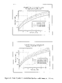
- Eqs. (70) and (71) are plotted as a function of frequency and energy spread in FIGS. 41-44 .
- the stored energy in the cavity is given by
- FIG. 45 a schematic diagram is shown of a power input scheme: a magnetron feeds energy into the rf cavity via a constant impedance tapered coaxial transmission line. Since rf power is fed radially inward from the perimeter of the cavity to the axis and experiences an increasing impedance, the voltage will increase on axis. This scenario is equivalent to a voltage step-up transformer.
Landscapes
- Particle Accelerators (AREA)
- Electron Sources, Ion Sources (AREA)
Abstract
Description
δ1δ2(1−T)>1 (1)
G=[δ 6δ2(1−T)](ωt/2π)
where π/ω is the half-period of the radian rf frequency ω. If there is a “seed” current density JS in the cavity at t=0, then at time t the current density will be given by
J=G J s =J s [δ1δ2(1−T)](ωt/2π)
until space-charge and resonance limit the current. The seed current density can be created by any of several sources including cosmic rays, a thermionic source, ultraviolet light, field emission, a spark, nuclear disintegration, etc. For a very low seed current density a high current density can be achieved in a very short time. For example, if δ=8, T=0.75, and Js=14×10−10 amps/cm2, at ten rf periods then J=1500 amps/cm2. Note: the remaining interior surface area (i.e. not surface S or the grid) of the cavity in
| TABLE I | ||||
| Material | δmax | εmax (keV) | ||
| GaAs + Cs (crystal) | 500 | (20 kev) | ||
| MgO (crystal) | 20-25 | (1.5 keV) | ||
| GaP + Cs (crystal) | 147 | (5.0 keV) | ||
where Z and A are the arithmetic mean atomic number and atomic weight, respectively. The secondary emission yield for GaP (
d 2 x/dt 2=(e/m)E 0 sinωt (5)
where f=ω/2π is the frequency of the cavity field. The instantaneous position x(t) and velocity dx/dt of the particle is readily solved from Eq.(5) to be
dz/dt=(eE 0 /mω)cosωt+C 1 (6)
and
x(t)=−(eE 0 /mω 2)sinωt+C 1 t+C 2 (7)
where C1 and C2 are constants of integration. This electron is assumed to originate at the electrode and have an initial velocity ν0 at a time wt=φ and a final velocity νf a half-cycle later ωt=σ+φ when it reaches the other electrode at x=d. If V0 is the peak applied rf voltage, d the electrode separation, it can easily be shown that resonance can occur if the voltage V0 satisfies
where the quantity Φ is given by
Φ(φ)=π cosφ+2 sinφ (9)
Note that Φ has a maximum value which gives rise to a minimum resonance condition. At the minimum resonance condition the phase angle φ is about 32.5°.
where the conditions at the opposite electrode x=d are now dx/dt=νf and ωt=φ−ωts+π. This gives
which is the analogue of the resonance condition Eq.(8) for finite secondary emission times. In the limit that the time between primary impact and secondary emission is much less than the rf frequency, ωts→0 (or more exactly ωts<<φ), result for resonance without a delay time is recovered. Specifically, for a delay time of 5 ps [P. T. Farnsworth, J. Franklin Institute, 218, 411 (1934)] and phase angle φ≈0.5 radians, the frequency should satisfy f<15.9 GHz.
3.4.3 Emittance and Oblique Secondary Emission
δ0 =Δexp(−αx m) (13)
where α is the fraction of electrons absorbed in the material per depth of penetration and Δ is the maximum yield. At an oblique angle θ of incidence then
δθ =Δexp(−αx m cosθ) (14)
Combining the previous two equations the following relation describing the yield for oblique incidence is obtained
δθ/δ0 =exp[αxm(1−cosθ)] (15)
where δ0 is the yield for a primary at normal incidence θ=π/2. Hence for oblique incidence of the primary beam there is an increase in secondary yield. This becomes noticeable for primary energies ε>εmax.
The results can be tabulated as follows:
| TABLE 2 |
| Probability for secondary electron emission at a given angle. |
| | probability | ||
| 0 < |θ| < 5 | 11% | ||
| 5 < |θ| < 15 | 21.5% | ||
| 15 < |θ| < 45 | 49% | ||
| 45 < |θ| < 75 | 17.5% | ||
| 75 < |θ| < 90 | 1% | ||
εn=2r b(kT t /mc 2)1/2 (17)
where kTt represents the average transverse kinetic energy, rb the beam radius and mc2 the electron rest mass energy. The secondary electron energy distribution typically has a spread of the order of an eV. Taking rb=0.5 cm, and since most of the particles come out at ˜300 then kTt is about 0.25 eV. From Eq.(17) the normalized emittance is 7 mm-mrad. This emittance is comparable to that achieved from thermionic emitters. The resonant secondary electrons become the primary electrons when they strike the opposite cavity wall. Since the angular distribution or emittance of the secondary electrons does not depend on the angle of incidence of the primary electrons then the emittance does not increase on successive periods inside the cavity.
with initial conditions
νf0(t=tf0), νb0(t=tb0), xf0, xf0(t=tf0), xb0(t=tb0)=0. The subscripts f and b refer to the front and back electrons and the top and bottom sign in Eq. (18), respectively. The quantities E0 and Esc are the magnitudes of the rf and space charge electric fields, respectively. Define the parameters
where Esc=neΔ/2ε0 and ε0 is the permittivity of free space. Then the solution of Eq. (18) is for velocity
and for position
where φ=arc tan(2/π)
Consider θb and theref ore the positive quantity in brackets in Eq. (22). If the space charge parameter αs is increased with all other parameters fixed, the back electron will go out of resonance when the quantity in brackets exceeds one. Thus to maintain resonance and the maximum space charge the following equation must be satisfied
where d is the gap length, V(t) is the (time-dependent) voltage at the opposite electrode, and j(0,t) is the current density at the source. Since dV/dt=V0ωcosωt, and V0˜ω2 (Eq.19), we find from the above equation that the current density scaling is indeed ∝ω3.
After evaluating Eq. (28) above
Note that if αs=0 then θf=θb and (Δ/d)FWHM=xf0/2d, as it should.
f=1.64E 2 exp(−8.5/E) (30)
where f is in MHz and E is the MV/meter. Enhancement due to the use of grid wires has not been included. However, because of advances in the cleaning and conditioning of surfaces, and also because of better vacuum techniques which produce high vacuum without the introduction of contaminants (e.g., diffusion pump oil, etc.), Kilpatrick's criterion overestimates the likelihood of breakdown by a factor of two or three for cw [R. A. Jameson, “RF Breakdown Limits,” in High-Brightness Accelerators, Plenum Press, 1988, p. 497] and five to six for short pulses [S. O. Schriber, Proc 1986 Linear Accelerator Conference, Jun. 2-6, 1986]. Hence, cavities operating at frequencies above Eq. (30) should be very safe from breakdown. For a cavity operating at 1.3 GHz, the critical electric field is ≈32 MV/meter. This is easily satisfied for a micropulse gun with gap lengths between 0.5 and 2.0 cm.
and ΔUE is the change in electric field energy, ΔUB is the change in magnetic field energy, and U is the stored energy in the cavity.
for a small beam radius, rb<<R,
For rb=1 cm, Δ/d=0.1, and R=8.83 cm (i.e., 1.3 GHz).
| TABLE 3 |
| Current densities at exit grid for cavity at 1.3 GHz. |
| voltage (kV) | Jx (kA/cm2) | ||
| 2.4 | 0.0026 | ||
| 2.8 | 0.008 | ||
| 4.3 | 0.02 | ||
| 6.4 | 0.04 | ||
| 9.8 | 0.0 | ||
where τd and fτ are the pulse duration and repetition rate, respectively, and τ is the FWHM of the current pulse. If T=75%, f=6.4 GHz, V0=105 keV, fτ=1 kHz and τd=100 ns then Pavg=210 watts/cm2. This is only 20% of the accepted relievable thermal load.
where IA=17βγ (kA). For the case of 6.4 GHz, α0=0.453, the electron energy is ε=(2/π)eV0 where V0=105 kV and Jx=2.8 kA/cm2. The required magnetic field is 4.8 kG. This is a tolerable field for a microwave generator.
T e=(4/√{square root over (4c−b 2)})(Ωc/ωp 2)
where Ωc=eB/m and the geometric factors c and b are expressed in the following form
b=l [(1−(r 1 /r 2)2]+└(r 2 /r c)2l−(r 1 /r 2)21┘−(r 1 /r c)2][1−(r 1 /r c)21]−[(1−(r 1 /r 2)21][(1−(r 2 (40)
and have defined r1, r2, rc to be the inner and outer beam radii and outer conductor radius respectively and l is the azimuthal mode number. The worst case to consider is for the l=2 mode. For the example parameters: n=6.25×1011 cm−3 (100 nC/cm3), B=4.5 kG, r1=2.68 cm, r2=3.04 cm and rc=3.09 cm, the e-folding time is about 2 nsec. This e-folding time allows a transport length of meters. This length is suitable for microwave generation.
where αα=eEα/mc and αsc=eEscImc. Eα and Esc are the accelerating and space charge electric fields, respectively. Note that Esc is the space charge field in the moving frame of the micro-pulse. The inductive electric field reduction of the space charge electric field is taken into account in Eq. (41) by the additional γ2. The equation for the time evolution of the length, s, of the micro-pulse is given by
where the subscript c refers to the center of the micro-pulse and the subscript f refers to the front or face of the micro-pulse. Define the change in γ from the front to the center of the micro-pulse by δγ=γf−γc. Assume that δγ/γc<<1, γc>>1, γf>>1. From Eqs (41), (42) definition of δγ the following pair of equations are obtained
where Δs, s0 are the change and initial length of the micro-pulse. For the example case at 6.4 GHz, s0=0.0625 cm (full length), γ0=1.1, Eα=20 MV/m and Esc=3 MV/m. The length change is 65% and the energy spread due to
where λ≡(2e/m)1/4/(9πJ)1/2. Integrating this expression gives φ (x) as a function of x in terms of the following cubic equation
ξ3−3bξ+(2b 3/2 −x/λ)=0 (49)
where b≡E0 2/16πJ(m/2e)1/2 and ξ=(b+√{square root over (φ)})1/2. Eq.(48) will be solved the physically interesting limit x/λb3/2>>1 which includes the space-charge-limited regime b∝E0 2→0. In this limit there is only one real root to Eq. (49), and the equation can be solved by trigonometric methods. The solution can be written in the form
Expanding Eq.(50) for large x/λb3/2 one obtains
φ(x)=b 2[(x/λb 3/2)2/3−1]2 (51)
V 0λ4/3 =r 4/3 cos(4θ/3)−2r 2/3 bλ 2/3 cos(2θ/3)+b 2λ4/3. (52)
For space-charge-limited emission, b=0, and Eq.(52) reduces to
V 0λ4/3 =r 4/3 cos4θ/3 (53)
For V0=0, the angle θ becomes the classical Pierce angle 3π/8=67.5°. By solving Eq. (52) for ρ=ρ(θ) where ρ=r(2πeJ/mc3)1/2 is the dimensionless polar coordinate, the electrode shape for x/λb3/2>>1 is determined from the equation
where ν=2(mc2/e)1/4/3√{square root over (b)} and is usually larger than unity for most experiments. For instance, if the cathode electric field E0 is measured in V/m and the current density J in A/cm2, then ν˜1.6×10⁶(J1/2/E0). Using the values [J. S. Fraser and R. L. Sheffield, IEEE J. Quantum Elec. QE-23, 1489 (1987); Proc. 9th Int'l FEL Conf., ed. P. Sprangle, C. M. Tang, and J. Walsh, North Holland Publishing, Amsterdam, (1988). R. L. Sheffield, E. R. Gray and J. S. Fraser, p.222; P. J. Tallerico, J. P. Coulon, LA-11189-MS (1988); P. J. Tallerico et al, Linac Proc. 528 (1989)], J=200 A/cm2 and E0=10 MeV/m, one obtains ν=2.2. For smaller electric fields at the cathode E0<MeV, ν is even larger. Note that for J=200 A/cm2, the normalized coordinate ξ˜0.217x for x in cm. The electrode shapes described by Eq. (54) are shown in
and for a hollow beam
Eq. (55) is plotted in
J(amps/cm 2)=21.25f 3(GHz)d(cm) (57)
From this, the current for a solid beam is
and for a hollow beam is
The current is a linear function of frequency so that the charge per pulse is independent of frequency.
and
IT=JAT (63)
and for a hollow beam is
so that for a solid beam the peak transmitted beam power is
and for a hollow beam is
The peak rf power required to resonantly drive the beam in the input cavity is given by
where V0 is the resonant cavity voltage, J is the peak steady-state current, and A is the emission area for the beam. For a one centimeter diameter solid beam with α0=0.453, d=0.5 cm, f=6.4 GHz, the peak power is 147 MM in the cavity. If the cavity is fed coaxially as shown in
and for a hollow beam is
where x0m are the zeros of J0 and Rm is the resonant cavity radius for the m-th mode. For f=6.4 GHz, m=2, d=0.5 cm the resonant peak electric field is 210 kV/cm for α00.453. The stored energy is U=6.06 milli-joules.
| TABLE 4 |
| One possible set of design parameters for each of the two |
| major applications. Those appended with a (*) have an assumed |
| transmission of 70%, while those denoted with a (**) have an assumed |
| post acceleration of 500 kV. |
| Application | Ingector | rf Generator | ||
| Configuration | (Solid Beam) | (Hollow Beam) | ||
| Beam Output* | 0.7 |
8 kA | ||
| Beam Charge* | 8 |
70 | ||
| Frequency | ||||
| 4 |
5 GHz | |||
| Beam Area | 0.7 |
9 cm2 | ||
| Cavity Gap | 10 |
5 mm | ||
| Micro-Pulse | 12 |
9 ps | ||
| Required |
7 |
70 MW | ||
| ΔE/ |
4% | 2% | ||
| Proposed Harmonic | n/a | |
||
| rf Output** | n/a | 2 GW | ||
Claims (7)
Priority Applications (1)
| Application Number | Priority Date | Filing Date | Title |
|---|---|---|---|
| US09/995,077 US7285915B2 (en) | 1994-12-01 | 2001-11-26 | Electron gun for producing incident and secondary electrons |
Applications Claiming Priority (2)
| Application Number | Priority Date | Filing Date | Title |
|---|---|---|---|
| US34804094A | 1994-12-01 | 1994-12-01 | |
| US09/995,077 US7285915B2 (en) | 1994-12-01 | 2001-11-26 | Electron gun for producing incident and secondary electrons |
Related Parent Applications (1)
| Application Number | Title | Priority Date | Filing Date |
|---|---|---|---|
| US34804094A Continuation | 1994-12-01 | 1994-12-01 |
Publications (2)
| Publication Number | Publication Date |
|---|---|
| US20030038603A1 US20030038603A1 (en) | 2003-02-27 |
| US7285915B2 true US7285915B2 (en) | 2007-10-23 |
Family
ID=23366402
Family Applications (1)
| Application Number | Title | Priority Date | Filing Date |
|---|---|---|---|
| US09/995,077 Expired - Fee Related US7285915B2 (en) | 1994-12-01 | 2001-11-26 | Electron gun for producing incident and secondary electrons |
Country Status (1)
| Country | Link |
|---|---|
| US (1) | US7285915B2 (en) |
Cited By (3)
| Publication number | Priority date | Publication date | Assignee | Title |
|---|---|---|---|---|
| US20080217562A1 (en) * | 2007-03-06 | 2008-09-11 | Ngk Insulators, Ltd. | Method for reforming carbonaceous materials |
| US20110304283A1 (en) * | 2010-06-11 | 2011-12-15 | The Goverment of the United States of America, as represented by the Secretary of the Navy | High Average Current, High Quality Pulsed Electron Injector |
| RU2488909C2 (en) * | 2011-07-06 | 2013-07-27 | Юрий Николаевич Лазарев | Method for generation of uhf range broadband electromagnetic radiation and device for its implementation |
Families Citing this family (3)
| Publication number | Priority date | Publication date | Assignee | Title |
|---|---|---|---|---|
| US7348569B2 (en) * | 2004-06-18 | 2008-03-25 | Massachusetts Institute Of Technology | Acceleration of charged particles using spatially and temporally shaped electromagnetic radiation |
| JP4653649B2 (en) * | 2005-11-30 | 2011-03-16 | 株式会社東芝 | Multi-beam klystron equipment |
| CN108514856A (en) * | 2018-06-04 | 2018-09-11 | 四川大学 | A kind of method and its device of microwave and ultraviolet light combination curing |
-
2001
- 2001-11-26 US US09/995,077 patent/US7285915B2/en not_active Expired - Fee Related
Cited By (4)
| Publication number | Priority date | Publication date | Assignee | Title |
|---|---|---|---|---|
| US20080217562A1 (en) * | 2007-03-06 | 2008-09-11 | Ngk Insulators, Ltd. | Method for reforming carbonaceous materials |
| US20110304283A1 (en) * | 2010-06-11 | 2011-12-15 | The Goverment of the United States of America, as represented by the Secretary of the Navy | High Average Current, High Quality Pulsed Electron Injector |
| US8564224B2 (en) * | 2010-06-11 | 2013-10-22 | The United States Of America, As Represented By The Secretary Of The Navy | High average current, high quality pulsed electron injector |
| RU2488909C2 (en) * | 2011-07-06 | 2013-07-27 | Юрий Николаевич Лазарев | Method for generation of uhf range broadband electromagnetic radiation and device for its implementation |
Also Published As
| Publication number | Publication date |
|---|---|
| US20030038603A1 (en) | 2003-02-27 |
Similar Documents
| Publication | Publication Date | Title |
|---|---|---|
| Nusinovich et al. | Recent progress in the development of plasma-filled traveling-wave tubes and backward-wave oscillators | |
| Burkhart et al. | A virtual‐cathode reflex triode for high‐power microwave generation | |
| US7285915B2 (en) | Electron gun for producing incident and secondary electrons | |
| Loza et al. | Experimental plasma relativistic microwave electronics | |
| Chen | Excitation of large amplitude plasma waves | |
| Mako et al. | A high-current micro-pulse electron gun | |
| Abubakirov et al. | Developing a high-current relativistic millimeter-wave gyrotron | |
| US4506229A (en) | Free electron laser designs for laser amplification | |
| Egorov et al. | Microwave generation power in a nonrelativistic electron beam with virtual cathode in a retarding electric field | |
| US6633129B2 (en) | Electron gun having multiple transmitting and emitting sections | |
| Lawson et al. | Reflections on the university of Maryland’s program investigating gyro-amplifiers as potential sources for linear colliders | |
| Singh et al. | Electron gun for gyrotrons | |
| Totmeninov et al. | Highly efficient X-band relativistic twistron | |
| Pakter et al. | Electron beam halo formation in high-power periodic permanent magnet focusing klystron amplifiers | |
| Ansari et al. | Studies of pulse shortening phenomena and their effects on the beam–wave interaction in an RBWO operating at low magnetic field | |
| Ginzburg et al. | Experimental observation of cyclotron superradiance | |
| Ginzburg et al. | Production of ultra-short high-power microwave pulses in Čerenkov backward-wave systems | |
| EP0809271A2 (en) | Electron gun | |
| Ginzburg et al. | Generation of high-power ultrashort electromagnetic pulses on the basis of effects of superradiance of electron bunches | |
| Dubinov et al. | Complex phase dynamics of overlimiting electron beams propagating in opposite directions | |
| Bratman et al. | Broadband gyro-TWTs and gyro-BWOs with helically rippled waveguides | |
| Korbly et al. | Design of a Smith-Purcell radiation bunch length diagnostic | |
| Miles et al. | Modelling of micromachined klystrons for Terahertz operation | |
| Danilov et al. | Multi-Megawatt KA-Band Relativistic Gyrotron with a Longitudinally Slotted Cavity and a TM-Type Operating Mode | |
| Chiadroni | Electron Sources and Injection Systems |
Legal Events
| Date | Code | Title | Description |
|---|---|---|---|
| FEPP | Fee payment procedure |
Free format text: PETITION RELATED TO MAINTENANCE FEES FILED (ORIGINAL EVENT CODE: PMFP); ENTITY STATUS OF PATENT OWNER: SMALL ENTITY |
|
| REMI | Maintenance fee reminder mailed | ||
| LAPS | Lapse for failure to pay maintenance fees | ||
| REIN | Reinstatement after maintenance fee payment confirmed | ||
| FEPP | Fee payment procedure |
Free format text: PETITION RELATED TO MAINTENANCE FEES GRANTED (ORIGINAL EVENT CODE: PMFG); ENTITY STATUS OF PATENT OWNER: SMALL ENTITY |
|
| FPAY | Fee payment |
Year of fee payment: 4 |
|
| SULP | Surcharge for late payment | ||
| FP | Lapsed due to failure to pay maintenance fee |
Effective date: 20111023 |
|
| PRDP | Patent reinstated due to the acceptance of a late maintenance fee |
Effective date: 20120104 |
|
| REMI | Maintenance fee reminder mailed | ||
| LAPS | Lapse for failure to pay maintenance fees | ||
| STCH | Information on status: patent discontinuation |
Free format text: PATENT EXPIRED DUE TO NONPAYMENT OF MAINTENANCE FEES UNDER 37 CFR 1.362 |
|
| STCH | Information on status: patent discontinuation |
Free format text: PATENT EXPIRED DUE TO NONPAYMENT OF MAINTENANCE FEES UNDER 37 CFR 1.362 |
|
| FP | Lapsed due to failure to pay maintenance fee |
Effective date: 20151023 |