US7280232B2 - Method and apparatus for measuring wafer thickness - Google Patents
Method and apparatus for measuring wafer thickness Download PDFInfo
- Publication number
- US7280232B2 US7280232B2 US10/946,450 US94645004A US7280232B2 US 7280232 B2 US7280232 B2 US 7280232B2 US 94645004 A US94645004 A US 94645004A US 7280232 B2 US7280232 B2 US 7280232B2
- Authority
- US
- United States
- Prior art keywords
- beams
- focus error
- thickness
- light beams
- determining
- Prior art date
- Legal status (The legal status is an assumption and is not a legal conclusion. Google has not performed a legal analysis and makes no representation as to the accuracy of the status listed.)
- Expired - Fee Related, expires
Links
- 238000000034 method Methods 0.000 title claims description 16
- 238000005259 measurement Methods 0.000 claims abstract description 16
- XUIMIQQOPSSXEZ-UHFFFAOYSA-N Silicon Chemical compound [Si] XUIMIQQOPSSXEZ-UHFFFAOYSA-N 0.000 claims description 9
- 229910052710 silicon Inorganic materials 0.000 claims description 9
- 239000010703 silicon Substances 0.000 claims description 9
- 235000012431 wafers Nutrition 0.000 description 37
- 238000005516 engineering process Methods 0.000 description 5
- 239000004065 semiconductor Substances 0.000 description 5
- 230000006870 function Effects 0.000 description 4
- 230000003287 optical effect Effects 0.000 description 3
- 239000000463 material Substances 0.000 description 2
- 238000004806 packaging method and process Methods 0.000 description 2
- 230000004044 response Effects 0.000 description 2
- 238000004458 analytical method Methods 0.000 description 1
- 201000009310 astigmatism Diseases 0.000 description 1
- 230000008901 benefit Effects 0.000 description 1
- 230000005540 biological transmission Effects 0.000 description 1
- 230000008859 change Effects 0.000 description 1
- 230000003750 conditioning effect Effects 0.000 description 1
- 239000013078 crystal Substances 0.000 description 1
- 238000004519 manufacturing process Methods 0.000 description 1
- 239000002184 metal Substances 0.000 description 1
- 230000008569 process Effects 0.000 description 1
- 230000000750 progressive effect Effects 0.000 description 1
- 230000001681 protective effect Effects 0.000 description 1
- 238000012876 topography Methods 0.000 description 1
Images


Classifications
-
- G—PHYSICS
- G01—MEASURING; TESTING
- G01B—MEASURING LENGTH, THICKNESS OR SIMILAR LINEAR DIMENSIONS; MEASURING ANGLES; MEASURING AREAS; MEASURING IRREGULARITIES OF SURFACES OR CONTOURS
- G01B11/00—Measuring arrangements characterised by the use of optical techniques
- G01B11/02—Measuring arrangements characterised by the use of optical techniques for measuring length, width or thickness
- G01B11/06—Measuring arrangements characterised by the use of optical techniques for measuring length, width or thickness for measuring thickness ; e.g. of sheet material
Definitions
- the present invention relates to means for measuring thickness of objects; more particularly, to method and apparatus for non-contact measurement of thickness; and most particularly, to method and apparatus for non-contact measuring the thickness of a planar object such as a silicon wafer or a flat panel display.
- Silicon wafers are important elements of the semiconductor industry. Such wafers typically are sawn from artificially-grown silicon crystals and require one or more surface finishing or conditioning operations, each of which causes progressive thinning of a wafer.
- a system is needed for acccurate measurement of wafer thickness, preferably a non-contact system. Such a system may also be useful for measuring thickness of other semiconductor elements such as bare silicon wafers, flat panel displays, and MEMS.
- a wafer starts at a thickness of approximately 0.8 mm and provides the building block for all of the processing leading to a wide range of electronic memory products.
- a finished wafer moves to a “backend” facility, which may be another plant in a different country.
- the wafer goes through a back-grinding process wherein material is removed from the wafer backside by grinding the back surface.
- the wafer thickness after backgrinding is typically between about 0.1 mm and about 0.3 mm, depending upon the final application.
- the factory segment of the industry consists of thinning, dicing, and packaging chips cut from the wafer.
- a non-contact means for measuring the thickness of a test object, and especially of a chip-bearing silicon wafer after backgrind, wherein the thickness measurement is highly accurate, wherein spatial resolution along the surface of the object is very high, and wherein the means is not affected by metallic or non-silicon components of a wafer.
- a system in accordance with the invention for non-contact measurement of thickness of a test object employs a generator for creating a light beam, preferably a laser beam.
- the beam is split into two identical input beams and directed conventionally by mirrors and beam splitters such that the two input beams are directly opposed, defining a test space for receiving an object to be measured.
- a calibration object of known thickness for example, an optical flat, when inserted into the test space causes first and second reflected beams to be reflected from first and second sides of the calibration object.
- the thickness of the calibration object should approximate the thickness of a test object to be subsequently measured.
- Each reflected beam is diverted through a conventional auto-focus means comprising an astigmatic lens assembly and a quad CCD sensor coupled to focussing means on the input beam, causing each input beam to be focussed on the test object, thereby defining first and second focal points in space.
- the focal points are a known distance apart, as dictated by the known thickness of the calibration object.
- the focus is locked and the calibration object is moved to a plurality of new locations along the input beams on either side of the focal points, thereby generating a plurality of positive and negative focus error signals for each beam which may be plotted against location to yield a focus error characteristic curve for each beam.
- the output may be provided as a look-up table, a graph, or preferably is stored in a computer for use with an appropriate algorithm.
- the calibration object is removed, and the system is ready for measurement of the thickness of an object such as a silicon wafer.
- the test object is inserted into the path of the input beams, creating thereby first and second focus error signals for the first and second reflected beams.
- An important advantage of the present system is that a very small focused spot may be used, on the order of about 1 ⁇ m.
- the wafer thickness can be readily measured to a very high degree of resolution in the presence of surface features. This can be very useful, for example, in characterizing so-called “bump wafers” which have small bumps all over the wafer for interconnect. This is a relatively new concept and is being used at present by some advanced fabricators.
- the bumps presently have diameters and spacings on the order of 100 ⁇ m, and the industry goal will be to reduce both. It is important to know what the base thickness of the wafer is in between the bumps. Prior art systems having relatively large optical focus spots are not suitable for bump wafer analysis. However, a system in accordance with the invention can scan across a wafer and can readily determine the base thickness of the wafer between the bumps.
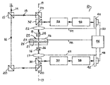
- FIG. 1 is a schematic drawing showing a system in accordance with the invention for measuring thickness of an object
- FIG. 2 is a graph of focus error signal as a function of distance from focus for use in a method in accordance with the invention
- FIG. 3 is a schematic drawing of a quad sensor when an input beam of the system shown in FIG. 1 is in focus on a surface of the object;
- FIG. 4 is a drawing like that shown in FIG. 3 , showing a C-D direction elliptical reflected beam when the focal point of the input beam is above the surface of the object;
- FIG. 5 is a drawing like that shown in FIG. 3 , showing a A-B direction elliptical reflected beam when the focal point of the input beam is below the surface of the object;
- FIG. 6 is a plurality of curves like that shown in FIG. 2 , taken at various objective powers of the system optics.
- a non-contact thickness measurement system 10 in accordance with the invention includes a light-generating source 12 capable of producing a master beam 14 .
- Beam 14 may be incoherent but preferably is a laser beam.
- a first beam splitter 15 divides master beam 14 into first and second input beams 16 , 18 which preferably are substantially identical in intensity.
- Angled mirrors 20 turn beams 16 , 18 such that they are in opposition along an optic axis 19 .
- First and second focussing means 17 , 22 are provided for focussing input beams 16 , 18 independently in a space 24 between focussing means 17 and 22 .
- first and second reflective beams 26 , 28 from surfaces 21 , 23 are turned by half-mirrors 30 , 32 , respectively, to direct reflective beams 26 , 28 through first and second lens 34 , 36 , first and second astigmatic systems 38 , 40 , and onto first and second quad cells 42 , 44 , respectively.
- a laser light discriminator (not shown) may also be included ahead of each quad cell in known fashion.
- a programmable control means 46 preferably a computer, including a selectively deactivatable autofocus algorithm, receives input signals 48 , 50 from quad cells 42 , 44 indicative of the focus state of input beams 16 , 18 with respect to surfaces 21 , 23 .
- Control means 46 sends output signals 52 , 54 to focussing means 17 , 22 to adjust the focus thereof until a null signal is produced in quad cells 42 , 44 .
- a conventional multi-axis stage 56 is provided in space 24 for mounting of object 25 and positioning object 25 in response to signals 58 from control means 46 .
- a conventional quad cell ( 42 or 44 ), as is known in the art, includes four phototransistor sensor quadrants, identified for convenience as A, B, C, and D.
- the lens combinations 34 , 36 and astigmatic systems 38 , 40 convert reflected circular beams 26 into astigmatic beams.
- the reflected beam impinging on the quad cell shows substantially no astigmatism and is circular ( 41 ), as shown in FIG. 3 . Because each quadrant produces an equal voltage output, there is a null balance among the quadrants, and the focus error signal is zero.
- the reflected beam assumes an oval shape ( 43 ) elongated in the C-D direction ( FIG. 4 ) providing a greater signal from C and D quadrants than from A and B quadrants.
- the focal point is above the reflective surface (i.e., outside the object)
- the reflected beam assumes an oval shape ( 45 ) elongated in the A-B direction ( FIG. 5 ) providing a greater signal from A and B quadrants than from C and D quadrants.
- the FES as a function of distance in both directions from a focal spot may be readily plotted by fixing the focus and then moving the reflective surface along optic axis 19 to a plurality of locations on either side of the focal spot.
- curve 60 When using an 80 ⁇ objective (curve 60 ), a distance resolution of about 0.1 ⁇ m can be obtained with system 10 .
- FES curves for this and other other objective magnifications are shown in FIG. 6 . Note the change in position scale (x-axis) between FIGS. 2 and 6 .
- a 20 ⁇ objective is used, providing a linear useful range of the 20 ⁇ curve ( 64 ) of about +/ ⁇ 40 ⁇ m from focal point 62 with a distance resolution of about 0.1 ⁇ m.
- system 10 is first calibrated.
- a calibration object 25 is positioned as shown in FIG. 1 .
- the calibration object is preferably a reference flat having plane parallel reflective surfaces 21 , 23 .
- the thickness of the calibration object is selected to approximate the estimated thickness of the test object.
- the objective power in focussing means 17 , 22 is also selected, based in part upon the topographic range to be measured in the test object and in part upon the accuracy required, as discussed above.
- the autofocus means in system 10 senses the degree of focus in quad cells 42 , 44 and adjusts focussing means 17 , 22 until a null signal is received from the quad cells.
- Input beams 16 , 18 are now in focus on surfaces 21 , 23 , respectively at first and second focal spots separated by a distance equal to the thickness of the calibration object, for example, 100 ⁇ m.
- the autofocus is then disabled, such that input beams remain in fixed focus on the first and second focal spots in space.
- Stage 56 is now moved along optic axis 19 , in response to signals 58 from control means 46 to stage 56 , to a plurality of locations on either side of the focal spots, as described above, thereby generating a plurality of focus error measurements as a function of the distance of each of the locations from the null location. These measurements preferably are stored in memory in control means 46 for later access. Stage 56 and calibration object 25 are returned to the focus null position, and the calibration object is removed.
- the test object is installed on stage 25 and positioned such that areas of surfaces 21 , 23 predetermined for measurement are positioned for impingement of input beams 16 , 18 . Because the focus of each beam 16 , 18 is now fixed, each quad cell 42 , 44 generates a focus error signal directly indicative of the distance, either positive or negative, of each surface 21 , 23 from the fixed focal points on optic axis 19 .
- the distances may be determined by referring to the calibration data previously stored in control means 46 . The distances are added to (positive distances) or subtracted from (negative distances) the calibration distance between the focal points, representing the thickness of the calibration object. Thus, the thickness of the test object is obtained.
- System 10 is especially useful in characterizing the thickness of objects of varying thickness, for example, a “bump” wafer having a gross wafer thickness at the peak of each bump and a net wafer thickness in the valleys between the bumps.
- Wafer 25 may be moved by control means 46 along a programmed path orthogonal to optic axis 19 . Because the size of each focal spot is small relative to the topography, the peak wafer thickness and valley wafer thickness may be readily determined.
Landscapes
- Physics & Mathematics (AREA)
- General Physics & Mathematics (AREA)
- Length Measuring Devices By Optical Means (AREA)
- Testing Or Measuring Of Semiconductors Or The Like (AREA)
Abstract
Description
FES=[(A+B)−(C+D)]/[A+B+C+D] (Eq. 1)
It will be seen that when A+B>C+D, the FES is positive, and when A+B<C+D, the FES is negative.
Claims (11)
Priority Applications (2)
| Application Number | Priority Date | Filing Date | Title |
|---|---|---|---|
| US10/946,450 US7280232B2 (en) | 2004-09-21 | 2004-09-21 | Method and apparatus for measuring wafer thickness |
| US11/388,316 US7283256B2 (en) | 2004-09-21 | 2006-03-24 | Method and apparatus for measuring wafer thickness |
Applications Claiming Priority (1)
| Application Number | Priority Date | Filing Date | Title |
|---|---|---|---|
| US10/946,450 US7280232B2 (en) | 2004-09-21 | 2004-09-21 | Method and apparatus for measuring wafer thickness |
Related Child Applications (1)
| Application Number | Title | Priority Date | Filing Date |
|---|---|---|---|
| US11/388,316 Continuation-In-Part US7283256B2 (en) | 2004-09-21 | 2006-03-24 | Method and apparatus for measuring wafer thickness |
Publications (2)
| Publication Number | Publication Date |
|---|---|
| US20060061775A1 US20060061775A1 (en) | 2006-03-23 |
| US7280232B2 true US7280232B2 (en) | 2007-10-09 |
Family
ID=36073585
Family Applications (1)
| Application Number | Title | Priority Date | Filing Date |
|---|---|---|---|
| US10/946,450 Expired - Fee Related US7280232B2 (en) | 2004-09-21 | 2004-09-21 | Method and apparatus for measuring wafer thickness |
Country Status (1)
| Country | Link |
|---|---|
| US (1) | US7280232B2 (en) |
Cited By (2)
| Publication number | Priority date | Publication date | Assignee | Title |
|---|---|---|---|---|
| US20080316504A1 (en) * | 2002-05-17 | 2008-12-25 | Gsi Lumonics Corporation | Method and system for machine vision-based feature detection and mark verification in a workpiece or wafer marking system |
| US20110235055A1 (en) * | 2010-03-25 | 2011-09-29 | Pat Buehler | System and method for measuring photovoltaic module thickness |
Citations (8)
| Publication number | Priority date | Publication date | Assignee | Title |
|---|---|---|---|---|
| US4201475A (en) * | 1977-05-18 | 1980-05-06 | Siemens Aktiengesellschaft | Device/process for contact free distance and thickness measurement |
| US4564296A (en) * | 1980-09-26 | 1986-01-14 | Hitachi, Ltd. | Plate thickness measuring method and apparatus |
| US4879706A (en) * | 1987-07-29 | 1989-11-07 | Laser Magnetic Storage International Company | Method and apparatus for focus and tracking in an optical disk system |
| US4910453A (en) * | 1987-10-15 | 1990-03-20 | Ade Corporation | Multi-probe grouping system with nonlinear error correction |
| US5351126A (en) * | 1991-10-31 | 1994-09-27 | Matsushita Electric Works, Ltd. | Optical measurement system for determination of an object's profile or thickness |
| US5696589A (en) * | 1996-05-20 | 1997-12-09 | Lockheed Martin Energy Systems, Inc. | Optical caliper with compensation for specimen deflection and method |
| US6111649A (en) * | 1998-10-12 | 2000-08-29 | Hitachi Denshi Kabushiki Kaisha | Thickness measuring apparatus using light from slit |
| US7119351B2 (en) * | 2002-05-17 | 2006-10-10 | Gsi Group Corporation | Method and system for machine vision-based feature detection and mark verification in a workpiece or wafer marking system |
-
2004
- 2004-09-21 US US10/946,450 patent/US7280232B2/en not_active Expired - Fee Related
Patent Citations (8)
| Publication number | Priority date | Publication date | Assignee | Title |
|---|---|---|---|---|
| US4201475A (en) * | 1977-05-18 | 1980-05-06 | Siemens Aktiengesellschaft | Device/process for contact free distance and thickness measurement |
| US4564296A (en) * | 1980-09-26 | 1986-01-14 | Hitachi, Ltd. | Plate thickness measuring method and apparatus |
| US4879706A (en) * | 1987-07-29 | 1989-11-07 | Laser Magnetic Storage International Company | Method and apparatus for focus and tracking in an optical disk system |
| US4910453A (en) * | 1987-10-15 | 1990-03-20 | Ade Corporation | Multi-probe grouping system with nonlinear error correction |
| US5351126A (en) * | 1991-10-31 | 1994-09-27 | Matsushita Electric Works, Ltd. | Optical measurement system for determination of an object's profile or thickness |
| US5696589A (en) * | 1996-05-20 | 1997-12-09 | Lockheed Martin Energy Systems, Inc. | Optical caliper with compensation for specimen deflection and method |
| US6111649A (en) * | 1998-10-12 | 2000-08-29 | Hitachi Denshi Kabushiki Kaisha | Thickness measuring apparatus using light from slit |
| US7119351B2 (en) * | 2002-05-17 | 2006-10-10 | Gsi Group Corporation | Method and system for machine vision-based feature detection and mark verification in a workpiece or wafer marking system |
Cited By (4)
| Publication number | Priority date | Publication date | Assignee | Title |
|---|---|---|---|---|
| US20080316504A1 (en) * | 2002-05-17 | 2008-12-25 | Gsi Lumonics Corporation | Method and system for machine vision-based feature detection and mark verification in a workpiece or wafer marking system |
| USRE41924E1 (en) | 2002-05-17 | 2010-11-16 | Gsi Group Corporation | Method and system for machine vision-based feature detection and mark verification in a workpiece or wafer marking system |
| US20110235055A1 (en) * | 2010-03-25 | 2011-09-29 | Pat Buehler | System and method for measuring photovoltaic module thickness |
| US8681345B2 (en) * | 2010-03-25 | 2014-03-25 | First Solar, Inc. | System and method for measuring photovoltaic module thickness |
Also Published As
| Publication number | Publication date |
|---|---|
| US20060061775A1 (en) | 2006-03-23 |
Similar Documents
| Publication | Publication Date | Title |
|---|---|---|
| KR100883386B1 (en) | Method and apparatus for precisely positioning the waste of a material processing laser beam to process microstructures within the laser processing site | |
| JP2002540422A (en) | High-speed measurement device for angle-dependent diffraction effects on microstructured surfaces | |
| CN114719765B (en) | Line Scan Knife-Edge Height Sensor for Semiconductor Inspection and Metrology | |
| US5338924A (en) | Apparatus and method for automatic focusing of light using a fringe plate | |
| US20240162074A1 (en) | Methods And Systems For Measurement Of Semiconductor Structures With Active Tilt Correction | |
| US7283256B2 (en) | Method and apparatus for measuring wafer thickness | |
| US7724375B1 (en) | Method and apparatus for increasing metrology or inspection tool throughput | |
| CN109631758A (en) | The detection device and detection method at sample center | |
| CN105103027A (en) | Measurement of focal points and other features in optical systems | |
| KR20140078621A (en) | Measuring form changes of a substrate | |
| CN114778514B (en) | Device and method for measuring non-destructive high aspect ratio structures based on Raman analysis | |
| CN114858419B (en) | A micro/nano grating diffraction angle measurement system and method | |
| US7280232B2 (en) | Method and apparatus for measuring wafer thickness | |
| JP2015232450A (en) | Film thickness measurement method and film thickness measurement device | |
| JPS63131116A (en) | confocal microscope | |
| KR20130010845A (en) | Charged particle beam drawing apparatus and method of manufacturing article | |
| JPH10253892A (en) | Phase interference microscope | |
| JP2002202108A (en) | Plate thickness measuring device | |
| JPH04162337A (en) | Electron beam device | |
| JP3967058B2 (en) | Method and apparatus for measuring surface shape and thickness of plate-like workpiece | |
| JPH0139041B2 (en) | ||
| JPS61223604A (en) | Gap measuring device | |
| JP2749900B2 (en) | Position detection method | |
| JP2000258339A (en) | Birefringence measurement device | |
| JPH0274804A (en) | Alignment apparatus |
Legal Events
| Date | Code | Title | Description |
|---|---|---|---|
| AS | Assignment |
Owner name: CHAPMAN INSTRUMENTS, NEW YORK Free format text: ASSIGNMENT OF ASSIGNORS INTEREST;ASSIGNORS:BRISTOW, THOMAS;WANG, SHU W.;REEL/FRAME:016244/0271 Effective date: 20050125 |
|
| STCF | Information on status: patent grant |
Free format text: PATENTED CASE |
|
| FPAY | Fee payment |
Year of fee payment: 4 |
|
| REMI | Maintenance fee reminder mailed | ||
| FPAY | Fee payment |
Year of fee payment: 8 |
|
| SULP | Surcharge for late payment |
Year of fee payment: 7 |
|
| FEPP | Fee payment procedure |
Free format text: MAINTENANCE FEE REMINDER MAILED (ORIGINAL EVENT CODE: REM.); ENTITY STATUS OF PATENT OWNER: SMALL ENTITY |
|
| LAPS | Lapse for failure to pay maintenance fees |
Free format text: PATENT EXPIRED FOR FAILURE TO PAY MAINTENANCE FEES (ORIGINAL EVENT CODE: EXP.); ENTITY STATUS OF PATENT OWNER: SMALL ENTITY |
|
| STCH | Information on status: patent discontinuation |
Free format text: PATENT EXPIRED DUE TO NONPAYMENT OF MAINTENANCE FEES UNDER 37 CFR 1.362 |
|
| FP | Lapsed due to failure to pay maintenance fee |
Effective date: 20191009 |