US7280121B2 - Image processing apparatus and method of same - Google Patents
Image processing apparatus and method of same Download PDFInfo
- Publication number
- US7280121B2 US7280121B2 US10/947,985 US94798504A US7280121B2 US 7280121 B2 US7280121 B2 US 7280121B2 US 94798504 A US94798504 A US 94798504A US 7280121 B2 US7280121 B2 US 7280121B2
- Authority
- US
- United States
- Prior art keywords
- pixel
- edge
- information
- memory
- aliasing
- Prior art date
- Legal status (The legal status is an assumption and is not a legal conclusion. Google has not performed a legal analysis and makes no representation as to the accuracy of the status listed.)
- Expired - Fee Related, expires
Links
Images


Classifications
-
- G—PHYSICS
- G06—COMPUTING OR CALCULATING; COUNTING
- G06T—IMAGE DATA PROCESSING OR GENERATION, IN GENERAL
- G06T17/00—Three-dimensional [3D] modelling for computer graphics
-
- G—PHYSICS
- G06—COMPUTING OR CALCULATING; COUNTING
- G06T—IMAGE DATA PROCESSING OR GENERATION, IN GENERAL
- G06T15/00—Three-dimensional [3D] image rendering
- G06T15/50—Lighting effects
- G06T15/503—Blending, e.g. for anti-aliasing
-
- G—PHYSICS
- G06—COMPUTING OR CALCULATING; COUNTING
- G06T—IMAGE DATA PROCESSING OR GENERATION, IN GENERAL
- G06T11/00—Two-dimensional [2D] image generation
-
- G—PHYSICS
- G06—COMPUTING OR CALCULATING; COUNTING
- G06T—IMAGE DATA PROCESSING OR GENERATION, IN GENERAL
- G06T11/00—Two-dimensional [2D] image generation
- G06T11/20—Drawing from basic elements
- G06T11/23—Drawing from basic elements using straight lines or curves
-
- G—PHYSICS
- G09—EDUCATION; CRYPTOGRAPHY; DISPLAY; ADVERTISING; SEALS
- G09G—ARRANGEMENTS OR CIRCUITS FOR CONTROL OF INDICATING DEVICES USING STATIC MEANS TO PRESENT VARIABLE INFORMATION
- G09G5/00—Control arrangements or circuits for visual indicators common to cathode-ray tube indicators and other visual indicators
- G09G5/36—Control arrangements or circuits for visual indicators common to cathode-ray tube indicators and other visual indicators characterised by the display of a graphic pattern, e.g. using an all-points-addressable [APA] memory
-
- G—PHYSICS
- G06—COMPUTING OR CALCULATING; COUNTING
- G06T—IMAGE DATA PROCESSING OR GENERATION, IN GENERAL
- G06T2200/00—Indexing scheme for image data processing or generation, in general
- G06T2200/12—Indexing scheme for image data processing or generation, in general involving antialiasing
Definitions
- the present invention relates to an image processing apparatus which expresses a model by a composite of unit graphics, generates pixel data in a drawing area of a screen coordinate system, performs rendering with respect to a memory, and, when generating an image, generates edge information and performs anti-aliasing and a method of the same.
- CG computer graphics
- three-dimensional graphics express the optical phenomenon when a three-dimensional object is illuminated by a predetermined light source by a mathematical model, add shading or gradation to the object surface based on this model, and further attach patterns to generate a more realistic and three-dimensional-like two-dimensional high definition image.
- Such computer graphics have become increasingly used in CAD/CAM in the field of development in science, engineering, and manufacture and other various fields of application.
- Three-dimensional graphic processing is generally composed by a “geometry sub-system” positioned as a front end and a “raster sub-system” positioned as a back end.
- the “geometry sub-system” means a step of geometric processing of the position, posture, etc. of a three-dimensional object displayed on a display screen.
- the geometry sub-system generally an object is handled as a set of a large number of polygons.
- the geometric processing such as “coordinate conversion”, “clipping”, and “light source computation” is carried out in unit of polygons.
- the “raster sub-system” means a step of painting pixels forming the object.
- the rasterization is realized by interpolating image parameters of all pixels included inside a polygon based on for example the image parameters found for each vertex of the polygon.
- the image parameters referred to here include color (drawing color) data expressed by a so-called RGB format, a z-value for expressing distance in a depth direction. etc.
- an f (fog) for fostering a sense of perspective and a texture t for expressing the feeling of the material or pattern of the object surface to impart realism are included as image parameters.
- the processing for generating a pixel inside a polygon from the vertex information of the polygon is often executed by using a linear interpolation technology referred to as a “digital differential analyzer” (DDA).
- DDA digital differential analyzer
- the inclination of data to a side direction of a polygon is found from the vertex information, the data on the side is calculated by using this inclination, the inclination of the raster scanning direction (X-direction) is calculated, and the amount of change of the parameter found from this inclination is added to the parameter value of the starting point of the scanning to thereby generate a pixel inside.
- rendering is performed for computing the color of each pixel and writing the value of this computed color to an address of a display buffer (frame buffer) corresponding to the pixel.
- the image generated by such computer graphics is anti-aliased or otherwise processed in order to raise the visual resolution since an aliasing effect of discontinuity of straight lines, polygonal edges, and boundaries of colors occurs. Extraction of the edge information becomes necessary for the anti-aliasing.
- edge extraction methods include the method of extracting edges from a generated picture by just filtering, the method of extracting edges by drawing polygons by outlines, etc. Further, the techniques of anti-aliasing include the super sampling method, the method of finding coverage for every pixel, etc.
- the method of extracting edges by just filtering does not utilize the advantages of the image being made by three-dimensional computer graphics, that is, useful data is generated etc. at the time of generating the image, so a certain degree of edge information is obtained, but edge information accurate enough to be able to be utilized for the anti-aliasing cannot be obtained.
- the super sampling method used as an anti-aliasing technique is a method of drawing a large amount of points and then applying a low pass filter (LPF).
- LPF low pass filter
- a first object of the present invention is to provide an image processing apparatus and method making unnecessary rendering of surrounding pixels other than in addition to the inherently necessary drawn pixels and capable of extracting edge information accurate enough to be able to be utilized for anti-aliasing without inducing a drop in the drawing speed.
- a second object of the present invention is to provide an image processing apparatus and method capable of realizing accurate anti-aliasing free from the influence of the drawing order and without inducing a drop in the drawing speed.
- an image processing apparatus generating pixel data inside a drawn area of a screen coordinate system to perform rendering with respect to a memory and generate an image drawn in the memory and, at that time, generating edge information and performing anti-aliasing, comprising an edge information extracting means for extracting the edge information based on predetermined pixel data drawn in the memory and an anti-aliasing means for determining the content of processing required for anti-aliasing based on the edge information obtained by the edge information extracting means and executing the determined processing.
- the anti-aliasing means determines adjoining pixels for blending with pixels on each edge and the blending ratio and performs blending based on the determined pixels and ratio.
- the anti-aliasing means includes a first means for detecting at which position of what shape of aliasing pattern a pixel being processed is at from the edge information and a second means for measuring a length from a start point of the detected aliasing pattern to the change point where the edge reverses and a length from the change point to where the aliasing pattern ends and calculating a position of a pixel to be blended with and a coefficient of blending based on information obtained from the first means and second means.
- the pixel data drawn in the memory includes depth information
- the edge information extracting means finds a second differentiation of the depth information obtained as a result of scanning a depth information buffer of the memory storing the depth information and extracts edge information based on the second differentiation.
- the data generated at the time of drawing to the memory includes a normal vector for every pixel, a normal vector buffer storing the normal vectors is formed in the memory, and the edge information extracting means extracts the edge information based on normal vectors obtained as a result of scanning the normal vectors for the pixels stored in the normal vector buffer.
- the pixel data drawn in the memory includes depth information
- the edge information extracting means restores the normal vector for each pixel from the depth information obtained as a result of scanning the depth information buffer of the memory storing the depth information and the screen coordinates and extracts the edge information based on the restored normal vectors.
- the edge information extracting means extracts edge information of a plurality of lines near a line being examined.
- an image processing method generating pixel data in a drawn area of a screen coordinate system to perform rendering with respect to a memory and generate an image drawn in the memory and, at that time, generating edge information and performing anti-aliasing, comprising a first step of extracting the edge information based on predetermined pixel data drawn in the memory and a second step of determining the content of processing required for anti-aliasing based on the edge information obtained at the first step and executing the determined processing.
- a depth information buffer is scanned, and a second differentiation of the depth information obtained by scanning.
- the edge information is extracted after for example drawing by utilizing information which is originally necessary at the time of ordinary drawing of three-dimensional computer graphics and remains as information when drawn, but is conventionally unused after that, for example, the information of the depth (z) buffer.
- information which does not remain in the ordinary drawing of three-dimensional computer graphics for example, the information of the normal vector for each pixel, is kept and used in later stages, or information necessary for the extraction of the edge at later stages is formed at the time of drawing and kept.
- the anti-aliasing means determines the value of which pixel adjoining each pixel on the edge in which direction and the blending ratio are determined and blending is performed by the determined value.
- FIG. 1 is a view of the system configuration of a three-dimensional computer graphic system forming an image processing apparatus according to the present invention
- FIGS. 2A and 2B are views for explaining second differentiation of a z-value according to the present embodiment
- FIGS. 3A to 3C are views for explaining a scanning operation of a z-buffer according to the present embodiment
- FIG. 4 is a view for explaining a method of restoring a normal vector by using the z-value according to the present embodiment
- FIGS. 5A to 5D are views for explaining a method of using a normal vector according to the present embodiment
- FIGS. 6A to 6D are views showing the most general patterns of edges needing anti-aliasing
- FIG. 7 is a view for explaining a blending operation in the anti-aliasing according to the present embodiment.
- FIG. 8 is a view for explaining a search method of an aliasing pattern according to the present embodiment.
- FIG. 9 is a view for explaining a method of finding overlapping edge patterns and suitably processing them when also acquiring edge information of a plurality of upper and lower lines other than a line in question at the time of line scanning according to the present embodiment
- FIG. 10 is a view for explaining a method of finding a pattern of a close edge and suitably processing the same when also acquiring edge information of a plurality of upper and lower lines other than a line in question at the time of line scanning according to the present embodiment;
- FIG. 11 is a view for explaining a method of finding a pattern of a close edge and suitably processing the same when also acquiring edge information of a plurality of upper and lower lines other than a line in question at the time of line scanning according to the present embodiment;
- FIG. 12 is a view for conceptually showing an example of the configuration of an anti-aliasing system according to the present embodiment
- FIGS. 13A to 13D are views for diagrammatically showing motion of a state machine and blending according to the present embodiment
- FIG. 14 is a view showing a case of changing an image on the memory for the RGB image as a result of rendering and transferring it to a display after the end;
- FIG. 15 is a view showing a case of raster scanning for displaying the RGB image as a result of rendering on a display and, in parallel and in synchronization with this, also scanning a z-buffer and, at the time of transfer to the display, changing the image on the memory and transferring it to the display after the end;
- FIGS. 16A to 16E are views for explaining edge extraction of a case of a boundary of adjacent planes.
- FIGS. 17A to 17D are views for explaining edge extraction of a case of a boundary between an object and a background.
- FIG. 1 is a view of the system configuration of a three-dimensional computer graphic system 10 forming an image processing apparatus according to the present invention.
- the three-dimensional computer graphic system 10 is a system for expressing a three-dimensional model as a composite of triangles (polygons) serving as unit graphics, drawing these polygons to decide the color of each pixel of the display screen, and displaying the result on a display, that is, for polygon rendering.
- the three-dimensional computer graphic system 10 uses, other to the (x, y) coordinates for expressing the position on a plane, a z-coordinate expressing the depth, so as to express a three-dimensional object and specifies any point in a three-dimensional space by the three (x, y, z) coordinates.
- the three-dimensional computer graphic system 10 performs image processing such as anti-aliasing on the image generated by the computer graphics.
- image processing such as anti-aliasing
- a large amount of useful information which cannot be utilized when ordinarily processing an image is generated in the step of generation of the computer graphics (CG) image.
- CG computer graphics
- a method of reusing or processing this useful information to accurately extract edge information indicating a surface on which a boundary or direction of an object in the image sharply changes is shown.
- the present embodiment includes two types of methods. Details will be explained later.
- the first method is the method of utilizing information which is originally necessary at the time of ordinary drawing of three-dimensional computer graphics and remains as information when drawn, but conventionally is not used after that, for example, the information of the z-buffer, to extracting edge information after the drawing.
- the information of the z-buffer is drawn by the three-dimensional computer graphics together with the color information, but conventionally while the color information is passed to the later stages for use, the z-information (z-value) is discarded without use after that.
- the information of the z-buffer is reused in the later stages.
- the second method is the method of keeping information which does not remain in ordinary drawing of three-dimensional computer graphics, for example information of the normal vector for every pixel and information of the inclination of the polygons, and using it in the later stages or the method of forming the information necessary for the edge extraction in the later stages and keeping the same.
- This method can be interpreted also as rendering an “instruction” or an “operation code” in the sense of indicating what should be done to later stages.
- the information is the information peculiar to three-dimensional computer graphics. It can also be said to be a technique for effectively processing and passing on to the later stages the information provided at the time of the drawing so that it can be used in the image processing of the latter stages.
- the second differentiation is calculated in units of pixels and used for the edge extraction.
- the inner products of the normal vectors of adjacent pixels are computed in units of pixels, and it is judged if a pixel is at an edge from the magnitude thereof.
- the three-dimensional computer graphic system 10 does not calculate and store the coverage of each pixel at the time of drawing unlike the generally used technique when performing the anti-aliasing. It does not use a technique such as multi-sampling and super sampling either.
- the three-dimensional computer graphic system 10 performs the anti-aliasing as post-processing after the end of the generation of the computer graphics image.
- the edge is extracted as post-processing after the end of the generation of the computer graphics image, and the anti-aliasing is carried out by utilizing the edge information.
- the pattern of the edge is derived from the edge information, and the pixels are processed in accordance with the pattern.
- the pixels surrounding the written pixel blended with not only are the pixels surrounding the written pixel blended with, but also both of the object and the background are blended with. Even pixels written as 100% in terms of coverage are sometimes blended.
- a linear long edge can be handled by using a state machine and a counter.
- a mounting method for scanning information of the z-buffer etc. in units of pixels and simultaneously proceeding with the anti-aliasing is also shown.
- the technique of applying the anti-aliasing to pixels by scanning either of the information of the z-buffer obtained at the time of the drawing or the information of the normal vector in each pixel or the information of both or by using the information of the normal vectors restored from the information of the z-buffer is employed.
- a state machine as a first means for holding the state and a counter as a second means for measuring continuity of the edge is prescribed.
- a counter as a second means for measuring continuity of the edge
- the decided value is used for the blending. This is successively performed during the scan until the pixel value is updated.
- the amount of the memory increased for the purpose of the anti-aliasing can be kept small, and no processing lowering performance at the time of the drawing is added.
- the three-dimensional computer graphic system 10 is comprised of a main processor 11 , a main memory 12 , an I/O interface circuit 13 , and a rendering circuit 14 connected via a main bus 15 .
- the rendering circuit 14 is connected to a CRT control circuit 16 . Note that, in FIG. 1 , the CRT control circuit 16 is provided outside the rendering circuit 14 , but a configuration providing the same in the rendering circuit 14 can also be employed.
- the rendering circuit 14 and/or CRT control circuit 16 constitute the edge information extracting means and the anti-aliasing means of the present invention.
- the main processor 11 reads out necessary graphic data from the main memory 12 in accordance with a state of progress etc. of the application and performs geometry processing etc. such as coordinate conversion, clipping, and lighting with respect to this graphic data to generate polygon rendering data.
- the main processor 11 outputs the polygon rendering data S 11 to the rendering circuit 14 via the main bus 15 .
- the I/O interface circuit 13 receives as input control information of motion or polygon rendering data etc. from the outside in accordance with need and outputs this to the rendering circuit 14 via the main bus 15 .
- the polygon rendering data input to the rendering circuit 14 includes data of (x, y, z, R, G, B ⁇ , s, t, q) of three vertexes of each polygon.
- (x, y, z) data shows the three-dimensional coordinates of the vertexes of the polygon
- (R, G, B) data shows luminance values of red, green, and blue at the three-dimensional coordinates.
- (s, t, q) data show homogeneous coordinates of a corresponding texture, and q shows a homogeneous term.
- “s/q” and “t/q” are multiplied with texture sizes USIZE and VSIZE to obtain actual texture coordinate data (u, v).
- Text data stored in a graphic memory of the rendering circuit 14 is carried out by using texture coordinate data (u, v).
- the polygon rendering data is physical coordinate values of vertexes of a triangle and colors of vertexes and texture data.
- the rendering circuit 14 has, as shown in FIG. 1 , a digital differential analyzer (DDA) set-up circuit 141 as an initial set-up operation block for a linear interpolation operation, a triangle DDA circuit 142 as a linear interpolation processing block, a texture engine circuit 143 , a memory interface (I/F) circuit 144 , and a graphic memory 145 configured by for example a DRAM.
- DDA digital differential analyzer
- a processing circuit is configured by the texture engine circuit 143 and the memory interface (I/F) circuit 144 .
- the DDA set-up circuit 141 finds a difference etc. between a side of the triangle and a horizontal direction for (z, R, G, B, ⁇ , s, t, q) data indicated by the polygon rendering data S 11 , that is, for a set-up operation.
- This set-up operation specifically calculates an amount of change of a value to be found in a case of a unit length movement by using the value of the start point, the value of the end point, and the distance between the start point and the end point.
- the DDA set-up circuit 141 outputs set-up data S 141 as information concerning a primitive, including the calculated change data, to the triangle DDA circuit 142 .
- the triangle DDA circuit 142 calculates the linearly interpolated (z, R, G, B, ⁇ , s, t, q) data at pixels inside the triangle based on the set-up data S 141 as the information concerning the primitive including the change data input from the DDA set-up circuit 141 .
- the triangle DDA circuit 142 outputs the (x, y) data of each pixel and the (z, R, G, B, ⁇ , s, t, q) data at the (x, y) coordinates as DDA data (interpolation data) S 142 to the texture engine circuit 143 .
- the triangle DDA circuit 142 interpolates the image parameters of all pixels included inside a polygon based on the image parameters found for every vertex of the polygon, that is, for rasterization.
- the triangle DDA circuit 142 rasterizes various types of data (z, texture coordinate, color etc.).
- the texture engine circuit 143 performs processing for calculation of “s/q” and “t/q”, processing for calculation of the texture coordinate data (u, v), reading of the (R, G, B) data from the graphic memory 145 , etc. in a pipeline format.
- the texture engine circuit 143 simultaneously performs the processing for a plurality of (for example four or eight) pixels positioned within for example a predetermined rectangle in parallel.
- the texture engine circuit 143 performs an operation for dividing the s data by the q data and dividing the t data by the q data for the (s, t, q) data indicated by the DDA data S 142 .
- the texture engine circuit 143 is provided with for example not shown a number of division circuits corresponding to the number (for example 8) of pixels to be processed in parallel.
- the divisions “s/q” and “t/q” for eight pixels are simultaneously carried out. Further, it is also possible to mount the circuit so as to perform the interpolation operation from a representative point among the 8 pixels.
- the texture engine circuit 143 multiplies the division results “s/q” and “t/q” with texture sizes USIZE and VSIZE to generate the texture coordinate data (u, v).
- the texture engine circuit 143 outputs a read request including the generated texture coordinate data (u, v) to the graphic memory 145 via the memory I/F circuit and reads out the texture data stored in the texture buffer included in the graphic memory 145 via the memory I/F circuit to thereby obtain the (R, G, B) data stored at the texture address corresponding to the (s, t) data.
- the texture engine circuit 143 generates the pixel data by multiplying etc. the (R, G, B) data of the read out (R, G, B) data and the (R, G, B) data included in the DDA data S 142 from the former triangle DDA circuit 142 to generate the pixel data.
- the texture engine circuit 143 finally outputs this pixel data as the color value of the pixel to the memory I/F circuit 144 .
- the texture buffer included in the graphic memory 145 stores MIPMAP (texture for a plurality of resolutions) or other texture data corresponding to a plurality of compression rates.
- MIPMAP texture for a plurality of resolutions
- which compression rate texture data to use is determined at the above triangular units using a predetermined algorithm.
- the texture engine circuit 143 directly uses the (R, G, B) data read out from the texture buffer in the case of a full color mode.
- the texture engine circuit 143 transfers the data of a color index table prepared in advance from a texture color look-up table (CLUT) buffer to a temporary storage buffer configured by a built-in SRAM etc. and obtains the (R, G, B) corresponding to the color index read out from the texture buffer by using this color look-up table.
- CLUT texture color look-up table
- the color look-up table is comprised of an SRAM
- the color index is input to the address of the SRAM
- the actual (R, G, B) data comes out in the output.
- the texture engine circuit 143 can be configured so as to store information which does not remain in ordinary drawing of three-dimensional computer graphics, for example, information of the normal vector for every pixel and information of the inclination of the polygon in the graphic memory 145 for realizing the second method of edge information extraction explained above.
- the memory I/F circuit 144 compares the z-data corresponding to the pixel data S 145 input from the texture engine circuit 143 and the z-data stored in the z-buffer included in the graphic memory 145 , judges whether or not the image drawn by the input pixel data is positioned closer (to the viewing point side) than the image written to the graphic memory 145 (display buffer) the previous time, and updates the z-data to the image data and stored in the z-buffer when it is positioned closer.
- the memory I/F circuit 144 writes the (R, G, B) data to the graphic memory 145 (display buffer).
- the memory I/F circuit 144 calculates the memory block of the graphic memory 145 storing the texture data corresponding to the texture address at the pixel to be drawn from then on from the texture address, issues a read request to only that memory block, and thereby read out the texture data.
- a memory block not retaining the corresponding texture data is not accessed for reading the texture data, so it becomes possible to provide more access time for drawing.
- the memory I/F circuit 144 reads out the pixel data from the corresponding address for modify writing of the memory block of the graphic memory 145 storing the pixel data corresponding to the pixel address to which the data is to be drawn from then on and writes back the data to the same address after the modification.
- the circuit reads out the depth data from the corresponding address for modify writing of the memory block storing the depth data corresponding to the pixel address to which the data is still be drawn as well and, if necessary, writes back the data to the same address after the modification.
- the memory I/F circuit 144 when receiving the read request including the generated texture coordinate data (u, v) with respect to the graphic memory 145 from the texture engine circuit 143 , reads out the (R, G, B) data stored in the graphic memory 145 .
- the memory I/F circuit 144 when receiving a request for reading the display data from the CRT control circuit 16 , the memory I/F circuit 144 reads out a certain amount of the display data, for example a unit of 8 pixels or 16 pixels, from the graphic memory 145 (display buffer) in response to this request.
- the memory I/F circuit 144 scans the graphic memory 145 (z-buffer) in the x-direction (horizontal direction) and the y-direction (vertical direction) to read out the z-value in response to this request.
- the memory I/F circuit 144 scans the graphic memory 145 to read out the normal vector information in response to this request.
- the memory I/F circuit 144 accesses (for writing or reading) the graphic memory 145 , but the write path and read path are configured as separate paths.
- the write address and the write data are processed in a write system circuit and written to the graphic memory 145 , while in the case of reading, they are processed in a read system circuit and read out from the graphic memory 145 .
- the memory I/F circuit 144 accesses the graphic memory 145 in units of for example 16 pixels based on a predetermined interleave type of addressing.
- the drawing performance can be improved by performing a number of the processings in parallel.
- simultaneous calculation is carried out for a plurality of pixels by providing the same circuit for the triangle DDA portion and the texture engine portion in a parallel valid format (space parallel) or finely inserting pipelines (time parallel).
- the memory blocks of the graphic memory 145 are arranged so that adjacent portions in the display region become different memory blocks as will be explained later, so when drawing a plane like a triangle, they become able to be simultaneously processed on the plane. Thus, the operation probability of each memory block becomes very high.
- the graphic memory 145 basically functions as the texture buffer, display buffer, z-buffer, and texture CLUT (Color Look Up Table) buffer.
- the graphic memory 145 functions also as a normal buffer for storing the normal vectors in addition to the functions as a texture buffer, display buffer, and z-buffer and the texture CLUT (Color Look Up Table) buffer.
- the graphic memory 145 is divided into a plurality of, for example four, modules having the same function.
- indexes at the index colors and the color look-up table values for the same are stored in the texture CLUT buffer.
- the indexes and color look-up table values are used for the texture processing as explained above.
- a texture element is normally expressed by a total 24 bits comprised of the 8 bits of each of R, G, and B. With this, however, the amount of data swells, so one color is selected from for example 256 colors selected in advance and that data is used for the texture processing. As a result, with 256 colors, a texture element can be expressed by 8 bits. A conversion table from the indexes to the actual colors becomes necessary, but the higher the resolution of the texture, the more compact the texture data can become.
- the graphic memory 145 stores the depth information of the object to be drawn for performing the hidden plane processing simultaneously and in parallel with the drawing.
- the display data is stored at a predetermined position in the memory block, for example continuously stored from the top, then the depth data is stored and then the texture data is stored in continuous address spaces for every type of the texture in the remaining vacant region.
- the final memory access becomes the drawing pixel unit such as a pixel.
- the CRT control circuit 16 generates a display address for display on a not shown CRT in synchronization with given horizontal and vertical synchronization signals and outputs a request for reading the display data from the display buffer included in the graphic memory 145 to the memory I/F circuit 144 .
- the memory I/F circuit 144 reads out a certain amount of the display data from the graphic memory 145 (display buffer).
- the CRT control circuit 16 includes for example a built-in FIFO circuit for storing the display data read out from the graphic memory 145 and generates the index value of RGB at constant time intervals.
- the CRT control circuit 16 stores the R, G, B data corresponding to the index values and transfers the R, G, B data of a digital format corresponding to the index values of generated RGB to a not illustrated digital/analog (D/A) converter to generate the R, G, B data of an analog format.
- D/A digital/analog
- the CRT control circuit 16 outputs this generated R, G, B data to a not shown CRT.
- the CRT control circuit 16 performs anti-aliasing and other the image processing with respect to the image generated by the computer graphics processing described above.
- the first method of reusing the z-value of the z-buffer and the second method of using the information of the normal vector for every pixel are employed.
- the z-value is originally calculated and written in the graphic memory 145 at the time of drawing of the three-dimensional computer graphics.
- the z-value itself is not used. Rather, second differentiation of the z-value becomes necessary.
- the second differentiation of the z-value is very useful information.
- a point where that value is off from the suitable threshold value can be regarded as an edge.
- the z-value calculated from the two-dimensional image by image recognition but the value of the accurate z is learned at the time of drawing the three-dimensional computer graphics, so the precision of the edge information detected from the second differentiation of z-value becomes extremely high.
- the edge obtained here is the boundary between the drawn object and the background in many cases.
- FIG. 2A at two points sandwiching the edge, the result (direction) of the second differentiation indicated by an arrow ⁇ 2 > in the drawing is very different from the results (directions) indicated by arrows ⁇ 1 > and ⁇ 3 > in the view inside the same object or at the background.
- FIG. 2B at two points sandwiching the edge, the result of the second differentiation indicated by the arrow ⁇ 3 > in the view is very different from the results (directions) indicated by arrows ⁇ 1 >, ⁇ 2 >, ⁇ 4 >, and ⁇ 5 > in the view inside the same object or background.
- a method of calculation by scanning the z-buffer after the end of drawing and a method of updating the second differentiation of z at the same timing as the writing (installation) of the pixel value at the time of the drawing can be employed.
- the latter method can be used to terminate the calculation of the second differentiation of z together with the drawing.
- a buffer of the second differentiations of z is provided other than the originally existing z-buffer and is initialized to 0. Whenever the z-value of a certain pixel is updated at the time of the drawing, the second differentiations of the surrounding pixels having z-values exerting an influence upon the second differentiation are updated.
- the buffer of the second differentiations of z is formed at the time of the end of drawing.
- Updating can be performed by a read modify write procedure of reading the value of d2z/dx20_, adding the above difference, and writing the result back.
- FIGS. 3A to 3C are views for explaining the method of scanning the z-buffer after the end of drawing and calculation to generate edge information as the method of obtaining the second differentiation of z.
- both of a scan in the horizontal direction (x-direction) and a scan in the vertical direction (y-direction) are effective for restoring the edge information, but it is also effective to make joint use of scans in both the vertical and horizontal directions in the anti-aliasing.
- Zth is an adjustable threshold value.
- the above processing can be made for each pixel by one scan of the z-buffer.
- Normal vectors are generated at the time of drawing, but are not ordinarily stored in the graphic memory 145 and are discarded after use. If storing them in the graphic memory 145 for every pixel, they can be used for the edge extraction in the later stages. The extraction method will be explained later.
- the vector obtained by normalizing the outer product of a vector from a certain point to two other points in a three-dimensional space formed by the three parameters of the value z of the z-buffer and the address (x, y) of the z-buffer is defined as a normal vector.
- the precision is raised if storing the value of the linearly interpolated normal vectors for Phong shading, but it is also possible to store a mean value of the polygon as the value at each pixel at the time of drawing not interpolating the normal vectors.
- FIGS. 5A to 5D show the method of extracting edge information from information of normal vectors.
- the information is extracted by the scanning either of the horizontal direction (x-direction) or the vertical direction (y-direction) or both.
- this normal vector buffer is scanned.
- the z-buffer When restoring a normal vector, the z-buffer is scanned and the normal vector is restored while judging edges.
- the inner products between the normal vector of the center pixel and the normal vectors of the pixels up, down, left and right of the pixel are obtained as shown in the diagram and the following equation 10.
- Px 0 N ( x,y ) ⁇ N ( x ⁇ 1 ,y )
- Px 1 N ( x,y ) ⁇ N ( x+ 1 ,y )
- Py 0 N ( x,y ) ⁇ N ( x,y ⁇ 1)
- Py 1 N ( x,y ) ⁇ N ( x,y+ 1) (10)
- nth is the adjustable threshold value. If the above inequality 11-1 or 11-2 is true, it is concluded that the pixel concerned is at an edge for the x-direction. If the above inequality 11-3 or 11-4 is true, it is concluded that the pixel concerned is at an edge for the y-direction.
- the inner products of the normal vectors of pixels adjacent to each other in both of the x- and y-directions are calculated. If the values of the inner products are within the range of from 1.0 to the threshold value, it is judged that the pixel is not at the edge, while if they are out of the range of the threshold value, it is judged that the pixel is at the edge.
- the information as to at which of the left or right or at which of the up or down an edge exists is added to the information as to whether a pixel is at the edge obtained as described above. Accordingly, as the information, in addition to 1 bit of information indicating existence of an edge, 1 bit of information indicating on which side the edge exists is necessary, so at least 2 bits of information are generated.
- the predetermined information is restored from the image after drawing the edge information for the x-direction and the y-direction in the screen coordinates, the processing content necessary for the anti-aliasing is determined from the obtained edge information, and the determined processing is carried out.
- the anti-aliasing is applied to each pixel.
- a state machine for holding the state and a counter for measuring the continuity of the edge are defined.
- ratio is the blending carried out with the pixel value of the adjacent pixel in which direction is determined.
- the determined value is for the blending. This is carried out successively during the scan until the pixel value is updated.
- the amount of increase of the memory used for the purpose of the anti-aliasing can be kept small, and processing lowering the performance at the time of drawing is not added.
- edges becoming aliased are the patterns shown in FIGS. 6A and 6C .
- the edges of such patterns are blended out as shown in FIGS. 6B and 6D .
- pixels sandwiching the edge are blended with each other.
- the area of a trapezoid in the figure when the length of the side of one pixel is 1.0 becomes the blend coefficient.
- the blend coefficients corresponding to the pixels are a 0 , a 1 , a 2 , b 0 , b 1 , and b 2 .
- a 0 ⁇ A 0*(1 ⁇ a 0)+ B 0 *a 0 B 0 ⁇ B 0*(1 ⁇ b 0)+ A 0 *b 0 a 0 3.0*0.5*0.5*(1 ⁇ 2*2/(3*3))
- b 0 3.0*0.5*0.5*(1 ⁇ 1/(3*3))
- a 1 ⁇ A 1*(1 ⁇ a 1)+ B 1 *a 1 B 1 ⁇ B 1*(1 ⁇ b 1)+ A 1 *b 1 a 1 3.0*0.5*0.5*2*2(3*3)*(1 ⁇ 1*1/(2*2))
- b 1 3.0*0.5*0.5*2*2(3*3)*(1 ⁇ 1*1/(2*2))
- a 2 ⁇ A 2*(1 ⁇ a 2)+ B 2 *a 2 B 2 ⁇ B 2*(1 ⁇ b 2)+ A 2 *b 2 a 2 3.0*0.5*0.5*(1*1/(3*3)) b
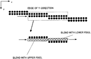
- the pixels which form the edge in the vertical direction in the related line are blended with either the upper or lower pixels forming the edge in the vertical direction and then are written back.
- the state machine shows at which position of which shape of pattern a pixel in processing is at, while the counter measures a length from the start point of the aliasing pattern to the change point (portion where upper and lower edges reverse) and a length from the change to when the aliasing pattern ends, for each pixel being processed.
- how many types of patterns can be recognized has an effect on the quality of the processing. Especially, it is necessary to find suitable processing for when two or more edges overlap or become close.
- the edge information of a plurality of upper and lower lines are also acquired in addition to that the related line at the time of the line scan. For example, in order to find the pattern of overlapped edges as shown in FIG. 9 and the close edges as shown in FIG. 10 and FIG. 11 and suitably process the same, it is necessary to simultaneously look at the information of at least two upper and two lower lines or five lines in total.
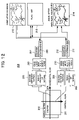
- FIG. 12 is a view conceptually showing a specific mode of mounting for realizing the edge information generation and the anti-aliasing explained above.
- This anti-aliasing system 200 has, as shown in FIG. 12 , a z-buffer 201 , a normal vector buffer 202 , a first second-differentiation circuit 203 for second differentiation of the z-value obtained by scanning the z-buffer 201 horizontally (in x-direction), a first inner product calculation circuit 204 for taking the inner product of the normal vectors obtained by scanning horizontally (in x-direction), a first edge judgment circuit 205 for edge judgment based on the results of the second differentiation circuit 203 and the inner product calculation circuit 204 , a first state machine 206 indicating at which position of which shape of pattern a pixel in processing exists based on the judgment result of the first edge judgment circuit 205 , a first counter 207 for measuring the length from the start point of the aliasing pattern to a change point (portion where upper and lower edges reverse) and the length from the change point to when the aliasing pattern ends, a second second-differentiation circuit 208 for second differentiation of the z
- the above “buffers” means memories of the data which each pixel has.
- the z-buffer 201 is a by-product of drawing as explained above and originally information which is discarded at the same time as the end of the drawing. In the present embodiment, this is reused.
- a normal vector can be restored by calculation from the z-buffer 201 and the screen coordinates, so a normal vector buffer is not necessary when that processing is included.
- the vertical scan and the horizontal scan are carried out simultaneously in parallel. Also, the processing is advanced together with each scan.
- the second differentiation of the z-value is found at the first and second second differentiation circuits 203 and 208 , and the inner product of the normal vectors of adjacent pixels is calculated at the first and second inner product calculation circuits 204 and 209 .
- the first and second edge judgment circuits 205 and 210 judge if the pixel concerned is at the edge for each of the x-direction and y-direction based on the results of the first and second second differentiation circuits 203 and 208 and the first and second inner product calculation circuits 204 and 209 and send the judgment results to the state machines 206 and 211 .
- the state machines 206 and 211 judge which portion of which pattern of edge the pixel in processing is at and hold the information of the edge. Then, the counters 207 and 212 measure the length of the edge.
- the state machines 206 and 211 and the counters 207 and 212 are cleared, the calculation of the blend coefficients, determination of the other pixels to be blended with, etc. are performed going back to the pixels behind the line, each pixel is blended, and the data is written in the display buffer serving as the memory for storing the image after processing.
- the pixel value of the “completed CG image” of the buffer 213 is blended with, while if it stands, the pixel value is read out from the “image after anti-aliasing” of the buffer 214 , that value is blended with, and then the data is written back.
- the width of the scan need only be three lines so as to detect an ordinary edge pattern, but it is necessary to simultaneously scan at least five lines in order to separate overlapped edges etc.
- the present invention does not exclude the possibility of any number of lines being simultaneously scanned as the plurality of lines.
- the state machine explained here uses three variables of “state”, “count”, and “parity”.
- “next#state” indicates a value next taken by the state.
- the scan advances by one pixel at a time in the scan direction.
- the z-buffer, normal buffer, or edge information buffer (meaning the memory storing the edge information obtained by the scan of the z-buffer etc.) is scanned in the x-direction and y-direction to change the variable “state” by the read data.
- the clearing of the counter, count up, and retention of values are determined in accordance with the variable “state”.
- FIGS. 13A to 13D When drawing the motion of the state machine and the blending by a figure, they become as shown in FIGS. 13A to 13D .
- the illustrated example is an example where the upper and side edges are viewed by the scan in the x-direction.
- the blending is carried out backward until the position when the variable state changes from 1 to 0.
- the value of the blend coefficient of the pixel having a larger count is a value near 0.5.
- the blending value of the pixel having a younger (smaller) count approaches a value near 0.
- the method of this calculation can be selected from a variety of methods.
- the method of making the blend coefficient of the pixel of the count C C/5*0.5 is the simplest method.
- a method of making the area of the trapezoid the blend coefficient as shown in for example FIG. 7 is possible.
- Len is 5 in the present example.
- the state machine performs processings in the x-direction and the y-direction. At each scan, a state machine is provided sensing the shape of the edge and the number of pixels is counted. As a result of the operation of the state machines, the pixels are processed backward.
- FIG. 14 and FIG. 15 are conceptual views of a case of complete post-processing after drawing using only the z-buffer.
- the CRT control circuit 16 of FIG. 1 accesses the graphic memory 145 through the memory I/F circuit 144 to scan the z-buffer and applies the anti-aliasing to each pixel by using the z-value information.
- FIG. 14 shows a case where the RGB image as the result of the rendering is changed on the memory by the CRT control circuit 16 and transferred to the display after that.
- FIG. 15 shows a case of raster scanning for displaying the RGB image as the result of the rendering on a display, in parallel and in synchronization, scanning the z-buffer and transferring the data to the display, and, at that time, changing the image on the memory by the CRT control circuit 16 and transferring the data to the display after the end.
- Both of FIG. 14 and FIG. 15 use only the z-buffer. No additional processing is used for the rendering. The entire processing is carried out as post-processing.
- edge information extraction specifically the following two types of edges are distinguished, and different processings are carried out.
- the first processing is the processing of the case of the boundary of the planes adjacent to each other as shown in FIG. 16 .
- the second processing is the processing of the case of the boundary between an object and the background as shown in FIG. 17 .
- the threshold values of the second differentiation of z are different between the first processing and the second processing.
- the blend coefficient is accurately found.
- the z-value of a 1 ⁇ 5+5 ⁇ 1 cross shape centered on the pixel concerned is read out.
- the blend coefficient is calculated simultaneously with this judgment.
- the second differentiation is used for the judgment.
- the second differentiation is independently calculated and used for the x-direction and y-direction.
- the information for the second processing is generated simultaneously with this first processing.
- the information of the 1 xn+nx 1 cross centered on the pixel concerned is read out.
- n is the mask.
- the information referred to here means the information generated in the first processing.
- the blend coefficient is calculated from that number.
- the edge extraction and the blending of the edge relating to the first processing are carried out. This processing is performed for all pixels by the 1 ⁇ 5+5 ⁇ 1 mask.
- Detecting the edge relating to the first processing (zdev and zdev 0 are used as threshold values) for the x- and y-directions.
- the blending of the edge relating to the second processing is carried out. This processing is performed for all pixels by the 1 xn+nx 1 mask . . . n is the mask length.
- the blend coefficient is made 0.
- the first loop and the second loop are independent loops.
- the mask n is 7.
- maskLen is 7 in FIG. 17 , and n here.
- the method comprises classifying the pixels so that there are as many gradations of the blend coefficients as possible for the pixels in the mask of the given mask, counting them, and finding the coefficients by using them.
- the graphic drawing and other data is given from the main memory 12 of the main processor 11 , or the I/O interface circuit 13 receiving the graphic data from the outside, to the rendering circuit 14 via the main bus 15 .
- the graphic drawing and other data is subjected to geometry processing such as the coordinate conversion, clipping, and lighting in the main processor 11 etc.
- the graphic data after the geometry processing becomes polygon rendering data S 11 comprised of the vertex coordinates, the x, y, and z of the vertexes of the triangle, luminance values R, G, and B, and the texture coordinates s, t, and q corresponding to the pixels to be drawn.
- This polygon rendering data S 11 is sequentially transferred to the DDA set-up circuit 141 of the rendering circuit 14 .
- the DDA set-up circuit 141 generates change data indicating the difference etc. between a side of the triangle and the horizontal direction based on the polygon rendering data S 11 .
- the triangle DDA circuit 142 uses the set-up data S 141 including the change data to calculate the linear interpolated (z, R, G, B, ⁇ , s, t, q) data at each pixel inside the triangle.
- this calculated (z, R, G, B, ⁇ , s, t, q) data and the (x, y) data of each of the vertexes of the triangle are output as the DDA data S 142 from the triangle DDA circuit 142 to the texture engine circuit 143 .
- the triangle DDA circuit 142 performs the rasterization for interpolating the image parameters (z, texture coordinate, color etc.) of all pixels included inside a polygon based on the image parameters found for the vertexes of the polygon.
- the texture engine circuit 143 performs the operation of dividing the s data by the q data and the operation of dividing the t data by the q data for the (s, t, q) data indicated by the DDA data S 142 . Then, it multiplies the division results “s/q” and “t/q” with the texture sizes USIZE and VSIZE to generate the texture coordinate data (u, v).
- the texture engine circuit 143 outputs a read request including the generated texture coordinate data (u, v) to the memory I/F circuit 144 and reads the (R, G, B) data stored in the graphic memory 145 via the memory I/F circuit 144 .
- the texture engine circuit 143 multiplies the (R, G, B) data of the read out (R, G, B) data and the (R, G, B) data included in the DDA data S 142 from the former triangle DDA circuit 142 to generate the pixel data.
- This pixel data is output from the texture engine circuit 143 to the memory I/F circuit 144 .
- the memory I/F circuit 144 compares the z-data corresponding to the pixel data input from the texture engine circuit 143 and the z-data stored in the z-buffer and judges whether or not the image drawn by the input pixel data S 145 is positioned closer (to the view point side) than the image written to the display buffer the previous time.
- the z-data stored in the z-buffer is updated by the z-data corresponding to the image data.
- the memory I/F circuit 144 writes the (R, G, B) data to the display buffer of the graphic memory 145 .
- the data to be written (including also update) is written to the predetermined memory in parallel via the write system circuit.
- the memory I/F circuit 144 calculates the memory block of the graphic memory 145 storing the texture corresponding to the texture address in the pixels to be drawn from then on by the texture address, issues the read request to only that memory block, and reads out the texture data.
- the pixel data is read out from the corresponding address of the memory block storing the pixel data corresponding to the pixel address to which the data is to be drawn from then on so as to perform a modify write operation and after the modify operation is written back to the same address.
- the depth data is read out from the corresponding address of the memory block storing the depth data corresponding to the pixel data to which the data is still to be drawn from then on for so as to perform a modify write operation and, if necessary, after the modify operation, is written back to the same address.
- the CRT control circuit 16 When displaying the image on a not shown CRT, the CRT control circuit 16 generates the display address in synchronization with the given horizontal and vertical synchronization frequencies and issues a request for transfer of the display data to the memory I/F circuit 144 .
- the memory I/F circuit 144 transfers a certain amount of the display data to the CRT control circuit 16 .
- the CRT control circuit 16 stores the display data in a not shown display use FIFO etc. and generates RGB index values of RGB at constant intervals.
- the CRT control circuit 16 stores the RGB values with respect to the RGB indexes inside it and transfers the RGB values for the index values to a not shown D/A converter.
- the RGB image as the result of rendering is changed on the memory by the CRT control circuit 16 and then transferred to the display.
- the RGB image as the result of rendering is raster scanned for the display and in parallel and in synchronization the z-buffer is scanned and, at the time of the transfer to the display, the image is changed on the memory by the CRT control circuit 16 , then transferred to the display.
- the edge judgment is carried out while restoring the normal vector by scanning the z-buffer.
- the vertical scan and the horizontal scan are carried out simultaneously in parallel with respect to for example the z-buffer.
- the processing is advanced together with the scans.
- the CRT control circuit 16 finds the second differentiation of the z-value in each scan and calculates the inner product of the normal vectors of pixels adjacent to each other inside.
- the state machine judges which portion of which pattern of edge the pixel in processing is at and holds the information of the edge. Then, the counter measures the length of the edge.
- the image after the blending is written to the display buffer serving as the storage memory.
- the pixel value of the buffer “completed CG image” is blended with.
- the pixel value is read out from the “image after the anti-aliasing”, blended with, then written back.
- processing is post-processing of the drawing, there is minimum additional processing requested with respect to the drawing itself. Additional processing is sometimes requested, but even in that case, the processing is not processing increasing the number of pixels covered, so the drawing speed is not made slower.
- the processing can be performed by just the information of the z-buffer which is always generated when drawing three-dimensional computer graphics, so the number of memories required does not increase.
- the rendering of pixels other than the inherently necessary drawn pixels, such as the surrounding pixels is unnecessary and edge information accurate enough to be able to be utilized for anti-aliasing can be extracted without inducing a drop in the drawing speed.
Landscapes
- Engineering & Computer Science (AREA)
- Physics & Mathematics (AREA)
- General Physics & Mathematics (AREA)
- Theoretical Computer Science (AREA)
- Computer Graphics (AREA)
- Geometry (AREA)
- Software Systems (AREA)
- Computer Hardware Design (AREA)
- Image Generation (AREA)
Abstract
Description
d2z/dx2(x,y)=z(x+1,y)+z(x−1,y)−2*z(x,y)
d2z/dy2(x,y)=z(x,y+1)+z(x,y−1)−2*z(x,y) (1)
d2z/dx20—0(x,y)=z0(x+1,y)+z0(x−1,y)−2*z0(x,y) (2)
d2z/dx21—1(x,y)=z0(x+1,y)+z1(x−1,y)−2*z0(x,y) (3)
d2z/
d2z=4*z(x,y)−z(x,y−1)−z(x,y+1)−z(x−1,y)−z(x+1,y)
d2zdx=2*z(x,y)−z(x−1,y)−z(x+1,y)
d2zdy=2*z(x,y)−z(x,y−1)−z(x,y+1) (5)
abs(dz2dx(x,y))>zth
abs(dz2dy(x,y))>zth (6)
x-direction d2zdx=z(x+1,y)+z(x−1,y)−2*z(x,y)
y-direction d2zdy=z(x,y+1)+z(x,y−1)−2*z(x,y) (7)
(nx0,ny0,nz0)=((x2,y2,z2)−(x0,y0,z0)×((x1,y1,z1)−(x0,y0,z0))
nx0=(y2−y0)*(z1−z0)−(z2−z0)*(y1−y0)
ny0=(z2−z0)*(x1−x0)−(x2−x0)*(z1−z0)
nz0=(x2−x0)*(y1−y0)−(y2−y0)*(x1−x0) (8)
nx=z(x+1,y)−z(x,y)
ny=z(x,y+1)−z(x,y)
nz=−1 (9)
Px0=N(x,y)·N(x−1,y)
Px1=N(x,y)·N(x+1,y)
Py0=N(x,y)·N(x,y−1)
Py1=N(x,y)·N(x,y+1) (10)
Abs(px0)<(1.0— nth) 11-1.
Abs(px1)<(1.0— nth) 11-2.
Abs(py0)<(1.0— nth) 11-3.
Abs(py1)<(1.0— nth) 11-4.
nx(x−1,y)*nx(x,y)+ny(x−1,y)*ny(x,y)+nz(x−1,y)*nz(x,y)<nth (12)
nx(x−1,y)*nx(x,y)+ny(x+1,y)*ny(x,y)+nz(x+1,y)*nz(x,y)<nth (13)
nx(x,y−1)*nx(x,y)+ny(x,y−1)*ny(x,y)+nz(x,y−1)*nz(x,y)<nth (14)
nx(x,y+1)*nx(x,y)+ny(x,y+1)*ny(x,y)+nz(x,y+1)*nz(x, y)<nth (15)
A0→A0*(1−a0)+B0*a0
B0→B0*(1−b0)+A0*b0
a0=3.0*0.5*0.5*(1−2*2/(3*3))
b0=3.0*0.5*0.5*(1−1/(3*3))
A1→A1*(1−a1)+B1*a1
B1→B1*(1−b1)+A1*b1
a1=3.0*0.5*0.5*2*2(3*3)*(1−1*1/(2*2))
b1=3.0*0.5*0.5*2*2(3*3)*(1−1*1/(2*2))
A2→A2*(1−a2)+B2*a2
B2→B2*(1−b2)+A2*b2
a2=3.0*0.5*0.5*(1*1/(3*3))
b2=3.0*0.5*0.5*(1−2*2/(3*3)) (16)
| Case of x-direction scan | ||
| When state==0 | ||
| if (pixel forming edge in y-direction) | ||
| next#state=1 | ||
| count=1; | ||
| if (pixel forming edge also in x- | ||
| direction) | ||
| parity=1; | ||
| else | ||
| parity=0; | ||
| else | ||
| next#state=0; | ||
| count=0; | ||
| When state==1 | ||
| if (pixel forming edge in y-direction) | ||
| next#state=1; | ||
| count=count+1; | ||
| else | ||
| next#state=0; | ||
| if (parity==pixel forming edge in | ||
| 1&&xdirection) | ||
| Blending going back by amount of pixels | ||
| of count when mode=2 | ||
| if (parity==not edge in 1&&xdirection) | ||
| Blending going back by amount of pixels | ||
| of count when mode=1 | ||
| if (parity==pixel forming edge in | ||
| 0&&xdirection) | ||
| Blending going back by amount of pixels | ||
| of count when mode=0 | ||
| if (parity==not edge in 0&&xdirection) | ||
| Nothing done | ||
blend coefficient=0.5*0.5/Len*(Len−C+1)2−(Len−C)2 (17)
s=(sz3+sz1−2*sz2)/(sd4−sz3−sz2+sz1) (18)
α=(number of black pixels−Len/(4*(Len+1)) (19)
Claims (13)
Applications Claiming Priority (2)
| Application Number | Priority Date | Filing Date | Title |
|---|---|---|---|
| JPP2003-334203 | 2003-09-25 | ||
| JP2003334203A JP2005100177A (en) | 2003-09-25 | 2003-09-25 | Image processing apparatus and method |
Publications (2)
| Publication Number | Publication Date |
|---|---|
| US20050068333A1 US20050068333A1 (en) | 2005-03-31 |
| US7280121B2 true US7280121B2 (en) | 2007-10-09 |
Family
ID=34191502
Family Applications (1)
| Application Number | Title | Priority Date | Filing Date |
|---|---|---|---|
| US10/947,985 Expired - Fee Related US7280121B2 (en) | 2003-09-25 | 2004-09-23 | Image processing apparatus and method of same |
Country Status (5)
| Country | Link |
|---|---|
| US (1) | US7280121B2 (en) |
| EP (1) | EP1519319A3 (en) |
| JP (1) | JP2005100177A (en) |
| KR (1) | KR20050030595A (en) |
| CN (1) | CN1674049A (en) |
Cited By (10)
| Publication number | Priority date | Publication date | Assignee | Title |
|---|---|---|---|---|
| US20050068326A1 (en) * | 2003-09-25 | 2005-03-31 | Teruyuki Nakahashi | Image processing apparatus and method of same |
| US20060119614A1 (en) * | 2004-11-15 | 2006-06-08 | Sharp Kabushiki Kaisha | Three dimensional graphics processing apparatus, image display apparatus, three dimensional graphics processing method, control program and computer-readable recording medium |
| US20060125842A1 (en) * | 2004-12-10 | 2006-06-15 | Kim Il-Do | Image interpolation device and method of preventing aliasing |
| US20070147684A1 (en) * | 2005-12-23 | 2007-06-28 | Xerox Corporation | Edge pixel identification |
| US20070146386A1 (en) * | 2005-12-23 | 2007-06-28 | Xerox Corporation | Anti-aliased tagging using look-up table edge pixel identification |
| US20100053202A1 (en) * | 2008-08-31 | 2010-03-04 | Chun-Wei Chen | Systems and methods of image processing including removal of discontinuous ramp and/or smoothing features |
| US7733354B1 (en) | 2007-05-31 | 2010-06-08 | Adobe Systems Incorporated | Anti-aliased rendering |
| US20110249901A1 (en) * | 2010-04-13 | 2011-10-13 | Vivante Corporation | Anti-Aliasing System and Method |
| US9973687B2 (en) * | 2016-06-08 | 2018-05-15 | Chiun Mai Communication Systems, Inc. | Capturing apparatus and method for capturing images without moire pattern |
| CN110473281A (en) * | 2018-05-09 | 2019-11-19 | 网易(杭州)网络有限公司 | Threedimensional model retouches side processing method, device, processor and terminal |
Families Citing this family (62)
| Publication number | Priority date | Publication date | Assignee | Title |
|---|---|---|---|---|
| US20060250414A1 (en) * | 2005-05-03 | 2006-11-09 | Vladimir Golovin | System and method of anti-aliasing computer images |
| US8269788B2 (en) * | 2005-11-15 | 2012-09-18 | Advanced Micro Devices Inc. | Vector graphics anti-aliasing |
| JP4693660B2 (en) * | 2006-03-10 | 2011-06-01 | 株式会社東芝 | Drawing apparatus, drawing method, and drawing program |
| GB2443858A (en) * | 2006-11-14 | 2008-05-21 | Sony Uk Ltd | Alias avoiding image processing using directional pixel block correlation and predetermined pixel value criteria |
| JP2008306512A (en) * | 2007-06-08 | 2008-12-18 | Nec Corp | Information providing system |
| US20090033671A1 (en) * | 2007-08-02 | 2009-02-05 | Ati Technologies Ulc | Multi-sample rendering of 2d vector images |
| US8294730B2 (en) * | 2007-09-04 | 2012-10-23 | Apple Inc. | Anti-aliasing of a graphical object |
| US20100013854A1 (en) * | 2008-07-18 | 2010-01-21 | Microsoft Corporation | Gpu bezier path rasterization |
| US9235876B2 (en) | 2009-03-02 | 2016-01-12 | Flir Systems, Inc. | Row and column noise reduction in thermal images |
| US9986175B2 (en) | 2009-03-02 | 2018-05-29 | Flir Systems, Inc. | Device attachment with infrared imaging sensor |
| US9843742B2 (en) | 2009-03-02 | 2017-12-12 | Flir Systems, Inc. | Thermal image frame capture using de-aligned sensor array |
| US9998697B2 (en) | 2009-03-02 | 2018-06-12 | Flir Systems, Inc. | Systems and methods for monitoring vehicle occupants |
| US10244190B2 (en) | 2009-03-02 | 2019-03-26 | Flir Systems, Inc. | Compact multi-spectrum imaging with fusion |
| WO2012170949A2 (en) | 2011-06-10 | 2012-12-13 | Flir Systems, Inc. | Non-uniformity correction techniques for infrared imaging devices |
| US9635285B2 (en) | 2009-03-02 | 2017-04-25 | Flir Systems, Inc. | Infrared imaging enhancement with fusion |
| USD765081S1 (en) | 2012-05-25 | 2016-08-30 | Flir Systems, Inc. | Mobile communications device attachment with camera |
| US9756264B2 (en) | 2009-03-02 | 2017-09-05 | Flir Systems, Inc. | Anomalous pixel detection |
| US9674458B2 (en) | 2009-06-03 | 2017-06-06 | Flir Systems, Inc. | Smart surveillance camera systems and methods |
| US9208542B2 (en) | 2009-03-02 | 2015-12-08 | Flir Systems, Inc. | Pixel-wise noise reduction in thermal images |
| US9517679B2 (en) | 2009-03-02 | 2016-12-13 | Flir Systems, Inc. | Systems and methods for monitoring vehicle occupants |
| US10757308B2 (en) | 2009-03-02 | 2020-08-25 | Flir Systems, Inc. | Techniques for device attachment with dual band imaging sensor |
| US9473681B2 (en) | 2011-06-10 | 2016-10-18 | Flir Systems, Inc. | Infrared camera system housing with metalized surface |
| US9948872B2 (en) | 2009-03-02 | 2018-04-17 | Flir Systems, Inc. | Monitor and control systems and methods for occupant safety and energy efficiency of structures |
| US9451183B2 (en) | 2009-03-02 | 2016-09-20 | Flir Systems, Inc. | Time spaced infrared image enhancement |
| US9716843B2 (en) | 2009-06-03 | 2017-07-25 | Flir Systems, Inc. | Measurement device for electrical installations and related methods |
| US9843743B2 (en) | 2009-06-03 | 2017-12-12 | Flir Systems, Inc. | Infant monitoring systems and methods using thermal imaging |
| US9756262B2 (en) | 2009-06-03 | 2017-09-05 | Flir Systems, Inc. | Systems and methods for monitoring power systems |
| US9819880B2 (en) | 2009-06-03 | 2017-11-14 | Flir Systems, Inc. | Systems and methods of suppressing sky regions in images |
| US10091439B2 (en) | 2009-06-03 | 2018-10-02 | Flir Systems, Inc. | Imager with array of multiple infrared imaging modules |
| US9292909B2 (en) | 2009-06-03 | 2016-03-22 | Flir Systems, Inc. | Selective image correction for infrared imaging devices |
| US9848134B2 (en) | 2010-04-23 | 2017-12-19 | Flir Systems, Inc. | Infrared imager with integrated metal layers |
| US9706138B2 (en) | 2010-04-23 | 2017-07-11 | Flir Systems, Inc. | Hybrid infrared sensor array having heterogeneous infrared sensors |
| US9207708B2 (en) | 2010-04-23 | 2015-12-08 | Flir Systems, Inc. | Abnormal clock rate detection in imaging sensor arrays |
| KR101032835B1 (en) * | 2010-07-21 | 2011-05-06 | 서울대학교산학협력단 | Scanline based rendering method and apparatus therefor in vector graphics technology |
| JP5620741B2 (en) * | 2010-08-06 | 2014-11-05 | キヤノン株式会社 | Information processing apparatus, information processing method, and program |
| CN109618084B (en) | 2011-06-10 | 2021-03-05 | 菲力尔系统公司 | Infrared imaging system and method |
| US9235023B2 (en) | 2011-06-10 | 2016-01-12 | Flir Systems, Inc. | Variable lens sleeve spacer |
| US10389953B2 (en) | 2011-06-10 | 2019-08-20 | Flir Systems, Inc. | Infrared imaging device having a shutter |
| US10079982B2 (en) | 2011-06-10 | 2018-09-18 | Flir Systems, Inc. | Determination of an absolute radiometric value using blocked infrared sensors |
| US10169666B2 (en) | 2011-06-10 | 2019-01-01 | Flir Systems, Inc. | Image-assisted remote control vehicle systems and methods |
| US10841508B2 (en) | 2011-06-10 | 2020-11-17 | Flir Systems, Inc. | Electrical cabinet infrared monitor systems and methods |
| US10051210B2 (en) | 2011-06-10 | 2018-08-14 | Flir Systems, Inc. | Infrared detector array with selectable pixel binning systems and methods |
| US9900526B2 (en) | 2011-06-10 | 2018-02-20 | Flir Systems, Inc. | Techniques to compensate for calibration drifts in infrared imaging devices |
| US9961277B2 (en) | 2011-06-10 | 2018-05-01 | Flir Systems, Inc. | Infrared focal plane array heat spreaders |
| US9706137B2 (en) | 2011-06-10 | 2017-07-11 | Flir Systems, Inc. | Electrical cabinet infrared monitor |
| US9058653B1 (en) | 2011-06-10 | 2015-06-16 | Flir Systems, Inc. | Alignment of visible light sources based on thermal images |
| WO2012170954A2 (en) | 2011-06-10 | 2012-12-13 | Flir Systems, Inc. | Line based image processing and flexible memory system |
| US9143703B2 (en) | 2011-06-10 | 2015-09-22 | Flir Systems, Inc. | Infrared camera calibration techniques |
| US9509924B2 (en) | 2011-06-10 | 2016-11-29 | Flir Systems, Inc. | Wearable apparatus with integrated infrared imaging module |
| EP2615834A1 (en) * | 2012-01-16 | 2013-07-17 | Thomson Licensing | Dealiasing method and device for 3D view synthesis |
| US9811884B2 (en) | 2012-07-16 | 2017-11-07 | Flir Systems, Inc. | Methods and systems for suppressing atmospheric turbulence in images |
| US9973692B2 (en) | 2013-10-03 | 2018-05-15 | Flir Systems, Inc. | Situational awareness by compressed display of panoramic views |
| US11297264B2 (en) | 2014-01-05 | 2022-04-05 | Teledyne Fur, Llc | Device attachment with dual band imaging sensor |
| RU2571574C1 (en) * | 2014-10-01 | 2015-12-20 | Федеральное Государственное Бюджетное Образовательное Учреждение Высшего Профессионального Образования "Донской Государственный Технический Университет" (Дгту) | Device to combine images into single composition with smooth contrast transition |
| CN105046729B (en) * | 2015-08-07 | 2017-09-26 | 浙江大学 | A kind of efficient parallel vector data method for visualizing |
| WO2021155000A1 (en) | 2020-01-29 | 2021-08-05 | ReportsNow, Inc. | Systems, methods, and devices for image processing |
| CN112184893B (en) * | 2020-10-15 | 2024-05-24 | 众智软件股份有限公司 | Line-surface body integrated drawing method, device, equipment and storage medium |
| US11158031B1 (en) | 2021-05-24 | 2021-10-26 | ReportsNow, Inc. | Systems, methods, and devices for image processing |
| WO2022250654A1 (en) * | 2021-05-24 | 2022-12-01 | Uiarmor.Com Llc | Systems, methods, and devices for image processing |
| US20230196627A1 (en) * | 2021-12-16 | 2023-06-22 | Meta Platforms Technologies, Llc | Anti-aliasing by encoding primitive edge representations |
| CN117710237B (en) * | 2022-08-30 | 2025-01-21 | 腾讯科技(深圳)有限公司 | Image anti-aliasing method, device, equipment, medium and program product |
| CN115690333B (en) * | 2022-12-30 | 2023-04-28 | 思看科技(杭州)股份有限公司 | Three-dimensional scanning method and system |
Citations (11)
| Publication number | Priority date | Publication date | Assignee | Title |
|---|---|---|---|---|
| US4780711A (en) | 1985-04-12 | 1988-10-25 | International Business Machines Corporation | Anti-aliasing of raster images using assumed boundary lines |
| US5123085A (en) | 1990-03-19 | 1992-06-16 | Sun Microsystems, Inc. | Method and apparatus for rendering anti-aliased polygons |
| EP0600709A2 (en) | 1992-12-01 | 1994-06-08 | Canon Kabushiki Kaisha | Range-image processing apparatus and method |
| US5325474A (en) * | 1990-10-23 | 1994-06-28 | Ricoh Company, Ltd. | Graphic output device including antialiasing capability governed by decisions regarding slope of edge data |
| US5668940A (en) | 1994-08-19 | 1997-09-16 | Martin Marietta Corporation | Method and apparatus for anti-aliasing polygon edges in a computer imaging system |
| US5903276A (en) * | 1995-03-14 | 1999-05-11 | Ricoh Company, Ltd. | Image generating device with anti-aliasing function |
| EP1094421A2 (en) | 1999-09-24 | 2001-04-25 | Nintendo Co., Limited | Method and apparatus for providing non-photorealistic cartoon outlining within a 3D videographics system |
| US20020167532A1 (en) | 1999-07-30 | 2002-11-14 | Stroyan Howard D. | System and method for reducing the effects of aliasing in a computer graphics system |
| US20030095134A1 (en) | 2000-11-12 | 2003-05-22 | Tuomi Mika Henrik | Method and apparatus for anti-aliasing for video applications |
| US6700672B1 (en) * | 1999-07-30 | 2004-03-02 | Mitsubishi Electric Research Labs, Inc. | Anti-aliasing with line samples |
| US6982723B1 (en) * | 1998-08-30 | 2006-01-03 | Gmd-Forschungszentrum Informationstechnik Gmbh | Method and apparatus for eliminating unwanted steps at edges in graphic representations in the line raster |
-
2003
- 2003-09-25 JP JP2003334203A patent/JP2005100177A/en active Pending
-
2004
- 2004-09-21 EP EP04255728A patent/EP1519319A3/en not_active Withdrawn
- 2004-09-23 US US10/947,985 patent/US7280121B2/en not_active Expired - Fee Related
- 2004-09-24 KR KR1020040076890A patent/KR20050030595A/en not_active Withdrawn
- 2004-09-25 CN CNA2004101037635A patent/CN1674049A/en active Pending
Patent Citations (11)
| Publication number | Priority date | Publication date | Assignee | Title |
|---|---|---|---|---|
| US4780711A (en) | 1985-04-12 | 1988-10-25 | International Business Machines Corporation | Anti-aliasing of raster images using assumed boundary lines |
| US5123085A (en) | 1990-03-19 | 1992-06-16 | Sun Microsystems, Inc. | Method and apparatus for rendering anti-aliased polygons |
| US5325474A (en) * | 1990-10-23 | 1994-06-28 | Ricoh Company, Ltd. | Graphic output device including antialiasing capability governed by decisions regarding slope of edge data |
| EP0600709A2 (en) | 1992-12-01 | 1994-06-08 | Canon Kabushiki Kaisha | Range-image processing apparatus and method |
| US5668940A (en) | 1994-08-19 | 1997-09-16 | Martin Marietta Corporation | Method and apparatus for anti-aliasing polygon edges in a computer imaging system |
| US5903276A (en) * | 1995-03-14 | 1999-05-11 | Ricoh Company, Ltd. | Image generating device with anti-aliasing function |
| US6982723B1 (en) * | 1998-08-30 | 2006-01-03 | Gmd-Forschungszentrum Informationstechnik Gmbh | Method and apparatus for eliminating unwanted steps at edges in graphic representations in the line raster |
| US20020167532A1 (en) | 1999-07-30 | 2002-11-14 | Stroyan Howard D. | System and method for reducing the effects of aliasing in a computer graphics system |
| US6700672B1 (en) * | 1999-07-30 | 2004-03-02 | Mitsubishi Electric Research Labs, Inc. | Anti-aliasing with line samples |
| EP1094421A2 (en) | 1999-09-24 | 2001-04-25 | Nintendo Co., Limited | Method and apparatus for providing non-photorealistic cartoon outlining within a 3D videographics system |
| US20030095134A1 (en) | 2000-11-12 | 2003-05-22 | Tuomi Mika Henrik | Method and apparatus for anti-aliasing for video applications |
Cited By (15)
| Publication number | Priority date | Publication date | Assignee | Title |
|---|---|---|---|---|
| US20050068326A1 (en) * | 2003-09-25 | 2005-03-31 | Teruyuki Nakahashi | Image processing apparatus and method of same |
| US7764292B2 (en) * | 2004-11-15 | 2010-07-27 | Sharp Kabushiki Kaisha | Three dimensional graphics processing apparatus, image display apparatus, three dimensional graphics processing method, control program and computer-readable recording medium |
| US20060119614A1 (en) * | 2004-11-15 | 2006-06-08 | Sharp Kabushiki Kaisha | Three dimensional graphics processing apparatus, image display apparatus, three dimensional graphics processing method, control program and computer-readable recording medium |
| US20060125842A1 (en) * | 2004-12-10 | 2006-06-15 | Kim Il-Do | Image interpolation device and method of preventing aliasing |
| US20070147684A1 (en) * | 2005-12-23 | 2007-06-28 | Xerox Corporation | Edge pixel identification |
| US7518618B2 (en) * | 2005-12-23 | 2009-04-14 | Xerox Corporation | Anti-aliased tagging using look-up table edge pixel identification |
| US7565015B2 (en) * | 2005-12-23 | 2009-07-21 | Xerox Corporation | Edge pixel identification |
| US20070146386A1 (en) * | 2005-12-23 | 2007-06-28 | Xerox Corporation | Anti-aliased tagging using look-up table edge pixel identification |
| US7733354B1 (en) | 2007-05-31 | 2010-06-08 | Adobe Systems Incorporated | Anti-aliased rendering |
| US20100053202A1 (en) * | 2008-08-31 | 2010-03-04 | Chun-Wei Chen | Systems and methods of image processing including removal of discontinuous ramp and/or smoothing features |
| US8115781B2 (en) * | 2008-08-31 | 2012-02-14 | Trident Microsystems (Far East) Ltd. | Systems and methods of image processing including removal of discontinuous ramp and/or smoothing features |
| US20110249901A1 (en) * | 2010-04-13 | 2011-10-13 | Vivante Corporation | Anti-Aliasing System and Method |
| US8554008B2 (en) * | 2010-04-13 | 2013-10-08 | Vivante Corporation | Anti-aliasing system and method |
| US9973687B2 (en) * | 2016-06-08 | 2018-05-15 | Chiun Mai Communication Systems, Inc. | Capturing apparatus and method for capturing images without moire pattern |
| CN110473281A (en) * | 2018-05-09 | 2019-11-19 | 网易(杭州)网络有限公司 | Threedimensional model retouches side processing method, device, processor and terminal |
Also Published As
| Publication number | Publication date |
|---|---|
| EP1519319A2 (en) | 2005-03-30 |
| JP2005100177A (en) | 2005-04-14 |
| EP1519319A3 (en) | 2006-05-10 |
| US20050068333A1 (en) | 2005-03-31 |
| KR20050030595A (en) | 2005-03-30 |
| CN1674049A (en) | 2005-09-28 |
Similar Documents
| Publication | Publication Date | Title |
|---|---|---|
| US7280121B2 (en) | Image processing apparatus and method of same | |
| EP1519317B1 (en) | Depth-based antialiasing | |
| CN108734624B (en) | Graphics processing pipeline including multiple processing stages and method and medium for operating the same | |
| US6961065B2 (en) | Image processor, components thereof, and rendering method | |
| US5704024A (en) | Method and an apparatus for generating reflection vectors which can be unnormalized and for using these reflection vectors to index locations on an environment map | |
| US7126600B1 (en) | Method and apparatus for high speed block mode triangle rendering | |
| US7570266B1 (en) | Multiple data buffers for processing graphics data | |
| US8044971B2 (en) | Methods of and apparatus for processing computer graphics | |
| US7884825B2 (en) | Drawing method, image generating device, and electronic information apparatus | |
| US6292192B1 (en) | System and method for the direct rendering of curve bounded objects | |
| KR100913459B1 (en) | Pixel center position displacement | |
| US20040012563A1 (en) | Systems and methods of multi-pass data processing | |
| US7742060B2 (en) | Sampling methods suited for graphics hardware acceleration | |
| US6424345B1 (en) | Binsorter triangle insertion optimization | |
| US20090046098A1 (en) | Primitive binning method for tile-based rendering | |
| US7554546B1 (en) | Stippled lines using direct distance evaluation | |
| US7038678B2 (en) | Dependent texture shadow antialiasing | |
| KR20140073480A (en) | Rendering a text image following a line | |
| US6184893B1 (en) | Method and system for filtering texture map data for improved image quality in a graphics computer system | |
| US5973701A (en) | Dynamic switching of texture mip-maps based on pixel depth value | |
| JP4977712B2 (en) | Computer graphics processor and method for rendering stereoscopic images on a display screen | |
| US6489966B1 (en) | Graphic processing device | |
| JP2003504697A (en) | Anti-aliasing of subsampled texture edges | |
| US7256796B1 (en) | Per-fragment control for writing an output buffer | |
| US7372461B2 (en) | Image processing apparatus and method of same |
Legal Events
| Date | Code | Title | Description |
|---|---|---|---|
| AS | Assignment |
Owner name: SONY CORPORATION, JAPAN Free format text: ASSIGNMENT OF ASSIGNORS INTEREST;ASSIGNORS:NAKAHASHI, TERUYUKI;WATANABE, OSAMU;NAGASAKI, TANIO;AND OTHERS;REEL/FRAME:015834/0296;SIGNING DATES FROM 20040817 TO 20040826 |
|
| FEPP | Fee payment procedure |
Free format text: PAYOR NUMBER ASSIGNED (ORIGINAL EVENT CODE: ASPN); ENTITY STATUS OF PATENT OWNER: LARGE ENTITY |
|
| FPAY | Fee payment |
Year of fee payment: 4 |
|
| REMI | Maintenance fee reminder mailed | ||
| LAPS | Lapse for failure to pay maintenance fees | ||
| STCH | Information on status: patent discontinuation |
Free format text: PATENT EXPIRED DUE TO NONPAYMENT OF MAINTENANCE FEES UNDER 37 CFR 1.362 |
|
| STCH | Information on status: patent discontinuation |
Free format text: PATENT EXPIRED DUE TO NONPAYMENT OF MAINTENANCE FEES UNDER 37 CFR 1.362 |
|
| FP | Lapsed due to failure to pay maintenance fee |
Effective date: 20151009 |