US7278121B2 - Method and apparatus for reducing redundant data in a layout data structure - Google Patents
Method and apparatus for reducing redundant data in a layout data structure Download PDFInfo
- Publication number
- US7278121B2 US7278121B2 US10/922,982 US92298204A US7278121B2 US 7278121 B2 US7278121 B2 US 7278121B2 US 92298204 A US92298204 A US 92298204A US 7278121 B2 US7278121 B2 US 7278121B2
- Authority
- US
- United States
- Prior art keywords
- interconnects
- bank
- data structure
- interconnect
- layout data
- Prior art date
- Legal status (The legal status is an assumption and is not a legal conclusion. Google has not performed a legal analysis and makes no representation as to the accuracy of the status listed.)
- Expired - Lifetime, expires
Links
Images


Classifications
-
- G—PHYSICS
- G06—COMPUTING OR CALCULATING; COUNTING
- G06F—ELECTRIC DIGITAL DATA PROCESSING
- G06F30/00—Computer-aided design [CAD]
- G06F30/30—Circuit design
- G06F30/39—Circuit design at the physical level
- G06F30/392—Floor-planning or layout, e.g. partitioning or placement
Definitions
- the present invention relates generally to a method and apparatus for data compression, and more particularly to a method and apparatus to reduce the size of a layout data structure.
- compression systems work by removing redundant or superfluous data in order to reduce the amount of data to be compressed. These systems often trade functionality and quality for higher compression ratios. Further, compression systems in general require significant computing power.
- U.S. Pat. No. 6,594,801 which issued to Dishon et al on Jul. 15, 2004, provides a method for compressing a data structure representing a layout of a multi layered VLSI device.
- the method comprises the steps of generating a non-functional elements locating data structure representing all the non-functional elements of all layers within the layout; deleting representations of non-functional elements from the data structure and adding the compressed non functional elements data structure to generate a compressed data structure representing the layout. While this technique does reduce the size of the layout data structure, it is a complex process requiring intensive computer power.
- the present invention is directed to a method and apparatus for reducing the data size of a layout data structure, by reducing the amount of electrically redundant interconnects within a bank of interconnects.
- These interconnect banks represent a unique signal within the layout.
- Electrically redundant interconnects are the repetitive interconnects within a bank of interconnects which do not contribute to the understanding of the IC. Therefore, a quantity of these interconnects may be deleted from the bank, provided that enough interconnects remain to maintain the electrical connectivity and the visual representation of a bank of interconnects.
- the data in a layout data structure is reduced by identifying interconnects within the layout, detecting banks of the interconnects, identifying selected interconnects located within the banks in accordance with a predetermined criteria and deleting the identified selected interconnects from the layout data structure.
- data in a layout data structure is reduced by assigning a unique address location to each interconnect within the layout file, detecting a bank of interconnects within the layout data structure using the unique addresses and replacing all the interconnects within the detected bank with a single large interconnect.
- the data in a layout data structure, having interconnects identified by coordinates in the layout file is reduced by assigning a unique address location to each interconnect within the layout data structure, using the unique addresses to detect banks of interconnects within the layout data structure, selecting locations within each bank where an interconnect will be flagged, sequentially identifying the location of each interconnect in the layout file, flagging the interconnects located in the predetermined locations and deleting the flagged interconnects from the layout data structure.
- the data in a layout data structure is reduced by assigning a unique address location to each interconnect within the layout data structure, detecting a bank of interconnects within the layout data structure using the unique addresses, deleting a plurality of the interconnects from the detected bank, leaving sufficient interconnects to maintain electrical connectivity and visual representation of said bank of interconnects.
- the unique address comprises bitwise interleaved x and y coordinates of the interconnect location in the layout.
- a bank of interconnects comprises the interconnects having a neighbouring interconnect located within a predetermined distance.
- interconnects that are selected for deletion may include the interconnects that border the outer edge of a bank, the interconnects that have interconnects on all sides, and/or the interconnects that are located in predetermined horizontal, vertical and/or diagonal rows in the bank.
- FIG. 1 is a schematic diagram of the apparatus in accordance with the present invention.
- FIG. 2 is a flow chart representation of the present invention
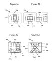
- FIGS. 3 a to 3 d are schematic representations of interconnect banks and demonstrate criteria for eliminating interconnects in a layout data structure
- FIG. 4 is a flow chart illustrating the selection of interconnects for retention and for elimination
- FIG. 5 is a schematic representation of producing a unique interconnect location code by interleaving.
- FIG. 6 is a histogram graph of interconnect frequency and distance measurements for determining banks of interconnects.
- the present invention provides a method to reduce the occurrence of redundant data within a layout data structure.
- this redundant data is found in the banks of repetitive structures such as interconnections, also referred to as vias or contacts, whereby multiple interconnects are contained within a small area and conduct the same electrical signal. These multiple interconnects use up valuable space within the layout data structure.
- the present invention reduces the data size by reducing the amount of electrically redundant interconnects within a bank of interconnects. Some of the interconnects within a bank do not contribute to the understanding of the IC. Therefore, a quantity of these interconnects may be deleted from the layout data of the bank, provided that enough interconnects remain to maintain the electrical conductivity and the visual representation of the bank. Data size reduction is particularly useful in applications such as, design emulation, circuit extraction, and in circuit layout design where only the visual representation of the data is needed.
- the method of the present invention may be implemented by the apparatus illustrated in the block diagram of FIG. 1 .
- the images of a delayered IC 2 may be captured by a microscopic imaging system 4 , such as a scanning electron microscope (SEM) or some other such device, and stored in a data storage memory 6 , which is coupled to a processor 8 .
- the images generated by the microscopic imaging system 4 are electronically stitched together to form grids of the mosaicked images. Pattern recognition is then performed on the images to generate the layout data structure, which is then aligned to ensure that the layers correspond correctly to each other.
- the aligned layout is stored in memory 6 with the original image files.
- a decimation algorithm 10 is applied to the layout data structure from storage 6 to produce a reduced layout data structure having a reduced amount of data.
- the reduced layout data structure is stored in data storage 12 .
- Interconnects are extracted 20 from the layout data structure stored in data storage 6 and banks of interconnects are detected 22 . Specific interconnects are then flagged 24 for deletion based on a predetermined criteria as provided by the decimation algorithm. These flagged interconnects are then deleted 26 from the layout data structure, resulting in a significant reduction in data size. The reduced data files for the banks of interconnects are then stored 28 in data storage 12 .
- FIGS. 3 a to 3 d Various criteria may be established for the decimation algorithm to determine which of the interconnects may be eliminated while maintaining the electrical connectivity as well as the visual representation of a bank of interconnects. Some of these criteria are demonstrated by FIGS. 3 a to 3 d.
- FIGS. 3 a and 3 b are graphical representations of 2 differently shaped interconnect banks 30 a and 30 b .
- the interconnects which border the edge of the bank 30 a and 30 b are designated as interconnects 32 a and 32 b respectively whereas the interconnects, which are completely surrounded by neighbouring interconnects and are shown as being contained within the thick dotted lines 34 a and 34 b respectively, are designated as interconnects 36 a and 36 b respectively.
- the lines 38 a and 38 b represent the edges of the interconnect banks 30 a and 30 b respectively.
- the criteria being applied for determining which interconnects are to be eliminated is whether or not an interconnect is completely surrounded by neighbouring interconnects.
- FIGS. 1 the criteria being applied for determining which interconnects are to be eliminated is whether or not an interconnect is completely surrounded by neighbouring interconnects.
- interconnects 36 a and 36 b are completely surrounded by other interconnects, therefore the criteria established may be that interconnects 36 a and 36 b are to be deleted from the banks 3 a and 3 b , leaving interconnects 32 a and 32 b . Alternately, interconnects 32 a and 32 b may be deleted leaving interconnects 34 a and 34 b in the banks. Therefore, in the method described in conjunction with FIG. 2 , the predetermined criteria for step 24 would be that either interconnects 34 a and 34 b are to be flagged for deletion or that interconnects 32 a and 32 b are flagged for deletion. As can be seen, by reducing the number of interconnects populating each bank 30 a , 30 b , the layout data structure size will be significantly reduced while the functionality of the bank of interconnections is maintained.
- FIGS. 3 c and 3 d Other alternative criteria in accordance with the present invention are demonstrated in FIGS. 3 c and 3 d .
- the interconnects 36 c in certain rows encircled by lines 34 c are to be flagged for deletion leaving interconnects 32 c .
- interconnects 32 c may be flagged for deletion, leaving interconnects 36 c .
- the example demonstrated in FIG. 3 d is similar to that described with respect to FIG. 3 c except that the interconnects 36 d enclosed by lines 34 d represent diagonal rows rather than vertical and horizontal rows.
- interconnects 36 d in certain diagonal rows encircled by lines 34 d are to be flagged for deletion leaving interconnects 32 d , or alternately, interconnects 32 d may be flagged for deletion, leaving interconnects 36 d .
- the interconnects are deleted in such a way that sufficient interconnects remain to maintain the electrical connectivity and visual representation of the bank. It should be quite clear from the above criteria examples that there are numerous ways of setting criteria to reduce the quantity of interconnects within a layout data structure in such a way that the remaining interconnects maintain the electrical connectivity as well as the visual representation of the bank.
- the interconnect location information may be used to identify the corners of an interconnect bank. With this information, all the interconnects within the bank may be replaced by a single large interconnect created to represent the entire bank. This large interconnect would substantially cover the entire area of the original interconnect bank, but require much less data to describe its location.
- the interconnects within the layout are identified 40 and the banks of interconnects detected 42 .
- a query is used to determine 44 if the interconnect of interest is within the bank in question. If not, the next interconnect is retrieved 46 . However, if the interconnect is within the bank in question, a second query determines 48 if the interconnect is required to maintain the electrical connectivity as well as the visual representation of the bank. If the response to the second query is yes, the interconnect is kept 50 and if the response is no, the interconnect is flagged 52 for deletion.
- the next interconnect is retrieved 46 and follows the same steps until all interconnects in the bank in question have been processed. As described with regard to FIG. 2 , step 26 , only the interconnects which have been flagged are then deleted from the layout data structure.
- the query in step 48 will depend on the criteria that has been set for keeping or deleting interconnects, for example, the query may be “is the interconnect on the edge of the bank?” as represented by FIGS. 3 a , 3 b , “is the interconnect in a predetermined row or column?” as represented by FIG. 3 c , or again “is the interconnect in a predetermined diagonal row?” as represented by FIG. 4 c . As described above, there may also be other criteria set, which would determine the form and content of the query.
- each interconnect has an x and y coordinate representative of its location within the layout.
- the coordinates of all interconnects within the layout are stored within memory 6 .
- these coordinates are then bitwise interleaved to form a unique number 55 representing the interconnect. This is done by combining the abscissa, the x coordinate X 1 and the ordinate, the y coordinate Y1 in the following way:
- the interleaving step is represented using an 8-bit interleaved coordinate, however a 64 bit co-ordinate is more likely for our application.
- all interconnect coordinates are interleaved and sorted. This sorting with the unique representation of the coordinates creates definable clusters in the array where blocks of interconnects are located. The distance between two successive interconnects within these clusters is computed and the data is used to create a histogram.
- the histogram graph of FIG. 5 represents the frequency at which interconnects are at a particular distance apart from other interconnects.
- a large peak 60 having a very high frequency 62 defines a bank of interconnects.
- the maximum frequency 62 in the histogram corresponds to the distance 64 between two interconnects in a bank, i.e.: the areas in which the interconnects are most densely populated would correspond to an interconnect bank, therefore, the distance between these interconnects would represent the maximum distance 64 between successive interconnects within a bank).
- the histogram data defines the maximum distance 64 between interconnects for a peak 60 of interconnects, it is possible to avoid confusion with interconnects which are located near to, but not within, a bank.
- interconnect bank The presence of neighbouring interconnects are identified and used to determine the outside boundaries of a bank, the interconnects within the bank or where within a bank a particular interconnect is located. As described above, this information is then used to determine which interconnects are to be deleted from the bank to reduce data in the layout data structure while at the same time maintaining the electrical connectivity and visual representation of the interconnect bank.
- One advantage of the present invention is that it reduces the data size of a layout data structure without the need for excessive computing power.
- Another advantage is that it provides a data size reduction without adversely affecting the layout quality or functionality.
Landscapes
- Engineering & Computer Science (AREA)
- Computer Hardware Design (AREA)
- Physics & Mathematics (AREA)
- Theoretical Computer Science (AREA)
- Architecture (AREA)
- Evolutionary Computation (AREA)
- Geometry (AREA)
- General Engineering & Computer Science (AREA)
- General Physics & Mathematics (AREA)
- Design And Manufacture Of Integrated Circuits (AREA)
Abstract
Description
- X1: x3x2x1x0 Y1: y3y2y1y0 to give interleaved address: x3y3x2
Claims (39)
Priority Applications (4)
| Application Number | Priority Date | Filing Date | Title |
|---|---|---|---|
| US10/922,982 US7278121B2 (en) | 2004-08-23 | 2004-08-23 | Method and apparatus for reducing redundant data in a layout data structure |
| CA2516827A CA2516827C (en) | 2004-08-23 | 2005-08-22 | Method and apparatus for reducing redundant data in a layout data structure |
| PL376727A PL376727A1 (en) | 2004-08-23 | 2005-08-23 | Method and appliance for reducing redundant data in the formatted data structure |
| CNB2005100937195A CN100495409C (en) | 2004-08-23 | 2005-08-23 | Method and apparatus for reducing redundant data in a layout data structure |
Applications Claiming Priority (1)
| Application Number | Priority Date | Filing Date | Title |
|---|---|---|---|
| US10/922,982 US7278121B2 (en) | 2004-08-23 | 2004-08-23 | Method and apparatus for reducing redundant data in a layout data structure |
Publications (2)
| Publication Number | Publication Date |
|---|---|
| US20060041849A1 US20060041849A1 (en) | 2006-02-23 |
| US7278121B2 true US7278121B2 (en) | 2007-10-02 |
Family
ID=35874849
Family Applications (1)
| Application Number | Title | Priority Date | Filing Date |
|---|---|---|---|
| US10/922,982 Expired - Lifetime US7278121B2 (en) | 2004-08-23 | 2004-08-23 | Method and apparatus for reducing redundant data in a layout data structure |
Country Status (4)
| Country | Link |
|---|---|
| US (1) | US7278121B2 (en) |
| CN (1) | CN100495409C (en) |
| CA (1) | CA2516827C (en) |
| PL (1) | PL376727A1 (en) |
Cited By (2)
| Publication number | Priority date | Publication date | Assignee | Title |
|---|---|---|---|---|
| US20070011628A1 (en) * | 2005-07-06 | 2007-01-11 | Semiconductor Insights Inc. | Method and apparatus for removing dummy features from a data structure |
| US20100325593A1 (en) * | 2009-06-18 | 2010-12-23 | Zavadsky Vyacheslav L | Integrated circuit analysis systems and methods |
Families Citing this family (4)
| Publication number | Priority date | Publication date | Assignee | Title |
|---|---|---|---|---|
| US8484599B2 (en) * | 2011-06-10 | 2013-07-09 | Synopsys, Inc. | Performing via array merging and parasitic extraction |
| WO2013033456A2 (en) | 2011-09-02 | 2013-03-07 | Board Of Trustees Of Michigan State University | Microbial nanowires and methods of making and using |
| CN111444667B (en) * | 2018-12-29 | 2023-03-21 | 杭州广立微电子股份有限公司 | Method for quickly deleting transistor data in GDSII file |
| US20210070811A1 (en) | 2019-09-05 | 2021-03-11 | Board Of Trustees Of Michigan State University | Method for protein nanowire synthesis and tunable control of nanowire length |
Citations (11)
| Publication number | Priority date | Publication date | Assignee | Title |
|---|---|---|---|---|
| US5587919A (en) * | 1994-04-22 | 1996-12-24 | Lucent Technologies, Inc. | Apparatus and method for logic optimization by redundancy addition and removal |
| US6091426A (en) | 1995-04-07 | 2000-07-18 | Intel Corporation | Integrating data scaling and buffering functions to minimize memory requirement |
| US6463576B1 (en) * | 1999-03-24 | 2002-10-08 | Nec Corporation | Method for designing an ASIC and ASIC designing apparatus |
| US20020166104A1 (en) * | 2000-12-14 | 2002-11-07 | Yu-Liang Wu | System and method for alternative wiring using pre-analyzed patterns |
| US6525722B1 (en) | 1995-08-04 | 2003-02-25 | Sun Microsystems, Inc. | Geometry compression for regular and irregular mesh structures |
| US6532581B1 (en) * | 1998-07-03 | 2003-03-11 | Matsushita Electric Industrial Co., Ltd. | Method for designing layout of semiconductor device, storage medium having stored thereon program for executing the layout designing method, and semiconductor device |
| US6594801B1 (en) | 2000-11-03 | 2003-07-15 | Motorola, Inc. | Method for compressing a data structure representing a layout of a VLSI device |
| US20030188271A1 (en) * | 2002-04-02 | 2003-10-02 | Institute Of High Performance Computing | System and method for integrated circuit design |
| US6742165B2 (en) * | 2001-03-28 | 2004-05-25 | Mips Technologies, Inc. | System, method and computer program product for web-based integrated circuit design |
| US6779158B2 (en) * | 2001-06-15 | 2004-08-17 | Science & Technology Corporation @ Unm | Digital logic optimization using selection operators |
| US6985847B2 (en) * | 1998-02-26 | 2006-01-10 | Micron Technology, Inc. | System and method for process matching |
-
2004
- 2004-08-23 US US10/922,982 patent/US7278121B2/en not_active Expired - Lifetime
-
2005
- 2005-08-22 CA CA2516827A patent/CA2516827C/en not_active Expired - Lifetime
- 2005-08-23 PL PL376727A patent/PL376727A1/en not_active Application Discontinuation
- 2005-08-23 CN CNB2005100937195A patent/CN100495409C/en not_active Expired - Lifetime
Patent Citations (11)
| Publication number | Priority date | Publication date | Assignee | Title |
|---|---|---|---|---|
| US5587919A (en) * | 1994-04-22 | 1996-12-24 | Lucent Technologies, Inc. | Apparatus and method for logic optimization by redundancy addition and removal |
| US6091426A (en) | 1995-04-07 | 2000-07-18 | Intel Corporation | Integrating data scaling and buffering functions to minimize memory requirement |
| US6525722B1 (en) | 1995-08-04 | 2003-02-25 | Sun Microsystems, Inc. | Geometry compression for regular and irregular mesh structures |
| US6985847B2 (en) * | 1998-02-26 | 2006-01-10 | Micron Technology, Inc. | System and method for process matching |
| US6532581B1 (en) * | 1998-07-03 | 2003-03-11 | Matsushita Electric Industrial Co., Ltd. | Method for designing layout of semiconductor device, storage medium having stored thereon program for executing the layout designing method, and semiconductor device |
| US6463576B1 (en) * | 1999-03-24 | 2002-10-08 | Nec Corporation | Method for designing an ASIC and ASIC designing apparatus |
| US6594801B1 (en) | 2000-11-03 | 2003-07-15 | Motorola, Inc. | Method for compressing a data structure representing a layout of a VLSI device |
| US20020166104A1 (en) * | 2000-12-14 | 2002-11-07 | Yu-Liang Wu | System and method for alternative wiring using pre-analyzed patterns |
| US6742165B2 (en) * | 2001-03-28 | 2004-05-25 | Mips Technologies, Inc. | System, method and computer program product for web-based integrated circuit design |
| US6779158B2 (en) * | 2001-06-15 | 2004-08-17 | Science & Technology Corporation @ Unm | Digital logic optimization using selection operators |
| US20030188271A1 (en) * | 2002-04-02 | 2003-10-02 | Institute Of High Performance Computing | System and method for integrated circuit design |
Non-Patent Citations (1)
| Title |
|---|
| Schroeder et al., "Decimation of Triangle Meshes," General Electric Company, Schenectady, NY. 1992. |
Cited By (8)
| Publication number | Priority date | Publication date | Assignee | Title |
|---|---|---|---|---|
| US20070011628A1 (en) * | 2005-07-06 | 2007-01-11 | Semiconductor Insights Inc. | Method and apparatus for removing dummy features from a data structure |
| US20080059920A1 (en) * | 2005-07-06 | 2008-03-06 | Semiconductor Insights Inc. | Method and apparatus for removing dummy features from a data structure |
| US7765517B2 (en) | 2005-07-06 | 2010-07-27 | Semiconductor Insights Inc. | Method and apparatus for removing dummy features from a data structure |
| US20100257501A1 (en) * | 2005-07-06 | 2010-10-07 | Semiconductor Insights Inc. | Method And Apparatus For Removing Dummy Features From A Data Structure |
| US7886258B2 (en) | 2005-07-06 | 2011-02-08 | Semiconductor Insights, Inc. | Method and apparatus for removing dummy features from a data structure |
| US8219940B2 (en) * | 2005-07-06 | 2012-07-10 | Semiconductor Insights Inc. | Method and apparatus for removing dummy features from a data structure |
| US20100325593A1 (en) * | 2009-06-18 | 2010-12-23 | Zavadsky Vyacheslav L | Integrated circuit analysis systems and methods |
| US8701058B2 (en) | 2009-06-18 | 2014-04-15 | Semiconductor Insights Inc. | Integrated circuit analysis systems and methods |
Also Published As
| Publication number | Publication date |
|---|---|
| CN100495409C (en) | 2009-06-03 |
| CA2516827C (en) | 2011-11-29 |
| PL376727A1 (en) | 2006-03-06 |
| CN1741024A (en) | 2006-03-01 |
| CA2516827A1 (en) | 2006-02-23 |
| US20060041849A1 (en) | 2006-02-23 |
Similar Documents
| Publication | Publication Date | Title |
|---|---|---|
| CA2517651C (en) | Method of design analysis of existing integrated circuits | |
| US7254270B2 (en) | System and method for bounding and classifying regions within a graphical image | |
| US7765517B2 (en) | Method and apparatus for removing dummy features from a data structure | |
| US6996794B2 (en) | Method of designing layout of semiconductor device | |
| Song et al. | Combining Models from Multiple Sources for RGB-D Scene Recognition. | |
| US6086238A (en) | Method and system for shape processing within an integrated circuit layout for parasitic capacitance estimation | |
| US7278121B2 (en) | Method and apparatus for reducing redundant data in a layout data structure | |
| US5761076A (en) | Method for evaluating a driving characteristic of a device for a wiring, based upon lower order coefficients of series expansion form of complex admittance of the wiring | |
| US5493509A (en) | Method of and apparatus for generating mask layouts | |
| US8423943B2 (en) | Self-propelling decoupling capacitor design for flexible area decoupling capacitor fill design flow | |
| JP2000200814A (en) | Failure distribution analysis system, method and recording medium | |
| Leu et al. | Detecting the spatial structure of natural textures based on shape analysis | |
| JP3904397B2 (en) | Table recognition method | |
| CN115828807B (en) | Netlist reduction method based on memory unit identification | |
| CN119071272A (en) | Method, device, storage medium and equipment for classifying grain failure bits | |
| CN113836878B (en) | Table generation method, device, electronic device and storage medium combining RPA and AI | |
| US6873726B2 (en) | Information adding apparatus, information extracting apparatus, information adding method, information extracting method, and computer readable recording medium | |
| CN113361545B (en) | Image feature extraction method, image feature extraction device, electronic equipment and storage medium | |
| US6819788B2 (en) | Failure analysis method that allows high-precision failure mode classification | |
| JP2573438B2 (en) | Pattern identification method and apparatus | |
| CN115035355B (en) | A Pixel Classification Method for Disconnected Regions of Binary Target Graph with Fifth Degree Search | |
| CN116467602B (en) | Training data generation method, device, computer equipment and storage medium | |
| CN1284188A (en) | Method and device for matching images | |
| Lee et al. | A region-based image retrieval system using salient point extraction and image segmentation | |
| Nikolopoulos et al. | Image replica detection using R-trees and linear discriminant analysis |
Legal Events
| Date | Code | Title | Description |
|---|---|---|---|
| AS | Assignment |
Owner name: SEMICONDUCTOR INSIGHTS INC., CANADA Free format text: ASSIGNMENT OF ASSIGNORS INTEREST;ASSIGNORS:KEYES, EDWARD;AITNOURI, ELMEHDI;BEGG, STEPHEN;AND OTHERS;REEL/FRAME:015871/0083;SIGNING DATES FROM 20040324 TO 20041224 |
|
| STCF | Information on status: patent grant |
Free format text: PATENTED CASE |
|
| FEPP | Fee payment procedure |
Free format text: PAYOR NUMBER ASSIGNED (ORIGINAL EVENT CODE: ASPN); ENTITY STATUS OF PATENT OWNER: LARGE ENTITY |
|
| CC | Certificate of correction | ||
| FPAY | Fee payment |
Year of fee payment: 4 |
|
| AS | Assignment |
Owner name: TECHINSIGHTS INC., CANADA Free format text: CHANGE OF NAME;ASSIGNOR:SEMICONDUCTOR INSIGHTS INC.;REEL/FRAME:033941/0692 Effective date: 20140821 |
|
| FPAY | Fee payment |
Year of fee payment: 8 |
|
| AS | Assignment |
Owner name: STELLUS CAPITAL INVESTMENT CORPORATION, AS ADMINISTRATIVE AGENT, TEXAS Free format text: NOTICE OF GRANT OF SECURITY INTEREST IN PATENTS;ASSIGNOR:TECHINSIGHTS INC.;REEL/FRAME:043571/0385 Effective date: 20170816 Owner name: STELLUS CAPITAL INVESTMENT CORPORATION, AS ADMINIS Free format text: NOTICE OF GRANT OF SECURITY INTEREST IN PATENTS;ASSIGNOR:TECHINSIGHTS INC.;REEL/FRAME:043571/0385 Effective date: 20170816 |
|
| MAFP | Maintenance fee payment |
Free format text: PAYMENT OF MAINTENANCE FEE, 12TH YEAR, LARGE ENTITY (ORIGINAL EVENT CODE: M1553); ENTITY STATUS OF PATENT OWNER: LARGE ENTITY Year of fee payment: 12 |
|
| AS | Assignment |
Owner name: CAPITAL ONE, NATIONAL ASSOCIATION, DELAWARE Free format text: SECURITY INTEREST;ASSIGNORS:TECHINSIGHTS INC.;VLSI RESEARCH INC.;REEL/FRAME:058096/0721 Effective date: 20211109 |
|
| AS | Assignment |
Owner name: TECHINSIGHTS INC., CANADA Free format text: RELEASE BY SECURED PARTY;ASSIGNOR:STELLUS CAPITAL INVESTMENT CORPORATION, AS ADMINISTRATIVE AGENT;REEL/FRAME:058096/0558 Effective date: 20211109 |