US7277828B2 - Methodology for designing high speed receivers below a target bit-error-rate - Google Patents
Methodology for designing high speed receivers below a target bit-error-rate Download PDFInfo
- Publication number
- US7277828B2 US7277828B2 US10/777,238 US77723804A US7277828B2 US 7277828 B2 US7277828 B2 US 7277828B2 US 77723804 A US77723804 A US 77723804A US 7277828 B2 US7277828 B2 US 7277828B2
- Authority
- US
- United States
- Prior art keywords
- processor
- voltage
- output voltage
- software
- Prior art date
- Legal status (The legal status is an assumption and is not a legal conclusion. Google has not performed a legal analysis and makes no representation as to the accuracy of the status listed.)
- Expired - Lifetime, expires
Links
Images


Classifications
-
- H—ELECTRICITY
- H04—ELECTRIC COMMUNICATION TECHNIQUE
- H04L—TRANSMISSION OF DIGITAL INFORMATION, e.g. TELEGRAPHIC COMMUNICATION
- H04L1/00—Arrangements for detecting or preventing errors in the information received
- H04L1/24—Testing correct operation
-
- H—ELECTRICITY
- H04—ELECTRIC COMMUNICATION TECHNIQUE
- H04L—TRANSMISSION OF DIGITAL INFORMATION, e.g. TELEGRAPHIC COMMUNICATION
- H04L1/00—Arrangements for detecting or preventing errors in the information received
- H04L1/20—Arrangements for detecting or preventing errors in the information received using signal quality detector
- H04L1/203—Details of error rate determination, e.g. BER, FER or WER
-
- H—ELECTRICITY
- H04—ELECTRIC COMMUNICATION TECHNIQUE
- H04L—TRANSMISSION OF DIGITAL INFORMATION, e.g. TELEGRAPHIC COMMUNICATION
- H04L25/00—Baseband systems
- H04L25/02—Details ; arrangements for supplying electrical power along data transmission lines
- H04L25/0202—Channel estimation
- H04L25/0212—Channel estimation of impulse response
Definitions
- the present subject matter relates in general to a methodology for designing high speed receivers. More particularly, the present subject matter relates to verifying the bit-error rate of a receiver design at various stages of the design process.
- a high speed serial data link is generally required to meet a customer-specified bit-error-rate (“BER”).
- BER bit-error-rate
- the BER of a receiver is tested and verified after the receiver has been designed and constructed. Having to re-work the design if the BER proves to be inadequate can be timely and costly.
- No direct method is known to exist to verify the BER of a receiver design at various stages of the design process.
- a method, and associated storage medium containing software and a system comprises extracting a time domain impulse response from parameters that characterize a communication channel, generating a probability distribution function (PDF) of an output voltage based on the impulse response; and computing a relationship between bit error rate and voltage margin based on the final probability distribution function.
- PDF probability distribution function
- Generating the PDF of the output voltage may comprise one or more of the following acts: quantizing the impulse response into a plurality of quantized levels, assigning taps to the quantized levels and determining a number of taps assigned to each quantized level, determining allowable voltage levels for each quantized level, and determining a probability of occurrence of each allowable voltage level, determining a PDF for each voltage level; and convolving all of the PDFs for the various voltage levels to obtain the PDF of the output voltage.
- the PDF is used to estimate the bit error rate of a receiver during the design process.
- FIG. 1 shows a communication system in which a transmitter sends information to a receiver over a channel
- FIG. 2 shows an exemplary method of computing the relationship between bit error rate and receiver sensitivity
- FIG. 3 illustrates an exemplary relationship between bit error rate and receiver sensitivity
- FIG. 4 shows an exemplary communication channel impulse response
- FIG. 5 shows illustrates an impulse response being quantized into a plurality of linearly spaced levels
- FIG. 6 shows an exemplary histogram of the number of taps assigned to each quantized level
- FIG. 7 shows the discrete voltage levels for a given tap level
- FIG. 8 shows an exemplary design process for a receiver during which the bit error rate of the design is evaluated at various stages of the design process.
- FIG. 1 shows a communication system in which a transmitter 10 sends information to a receiver 15 over a channel 12 .
- the transmitter 10 and receiver 15 can be any type of device and the channel 12 represents the physical medium over which the information between transmitter and receiver is transmitted.
- the transmitter 10 , receiver 15 , and channel 12 are implemented in a network switch in which digital data communications are routed between ports on the switch.
- the channel 12 may comprise a copper backplane.
- the channel 12 distorts the transmitted data, particularly at higher frequencies.
- the receiver 15 preferably has sufficient voltage sensitivity so as to accurately detect data bits transmitted to the receiver from the channel within a desired bit error rate (“BER”).
- BER bit error rate
- the desired BER is application specific generally given the goals and objectives of the operator of the communication system.
- the receiver preferably is designed to achieve the desired BER given the particular channel 12 interconnecting the transmitter and receiver.
- a methodology for verifying that the receiver 15 will achieve the desired BER at various stages of the receiver's design.
- An assessment of the receiver's voltage sensitivity is determined at various stages of the design.
- “sensitivity” refers to the minimum voltage increment a receiver is capable of resolving. For example, a sensitivity of 45 mv means that the receiver cannot resolve voltages in less than 45 mv increments. From the sensitivity value, the BER that the receiver will achieve for the determined sensitivity is computed. This computed BER may be higher than, lower than or equal to the desired BER and adjustments can be made to the design as necessary.
- FIG. 2 illustrates a preferred method for determining the relationship between BER and receiver voltage sensitivity such as that shown in the example of FIG. 3 .
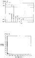
- BER is on the vertical access and sensitivity is on the vertical access.
- the BER also improves. For example, for a sensitivity of 45 millivolts (mv), the BER is 10 ⁇ 15 . That is, for a receiver that cannot resolve voltages in less than 45 mv increments, the receiver will receive one bit in error for every 10 15 bits received.
- the method begins generally at 52 in which the time domain impulse response of the channel 12 is extracted from s-parameters that characterize the channel.
- the s-channel characterization of the channel 12 can be measured using a network analyzer as would be well known to those of ordinary skill in the art.
- a tool such as MATLAB can be used to generate an impulse response of the channel and a finite impulse response (“FIR”) can be implemented in Verilog to model the channel.
- FIR finite impulse response
- an input impulse can be run through the Verilog modeled channel to compute the channel's impulse response.
- the time domain impulse response can be extracted in accordance with any suitable technique. An exemplary time domain impulse response is shown in FIG. 4 .
- the time domain impulse response preferably is linearly quantized.
- FIG. 5 shows an example in which an impulse response is quantized into a plurality of linearly spaced levels 80 .
- the various taps 82 of the impulse response are assigned to the various quantized levels 80 .
- a histogram such as that shown in FIG. 6 , can be constructed showing the number of taps 82 assigned to each quantized level
- the number of filter taps in each level are tallied (block 58 ).
- all allowable bit sequences for a given level should be considered. Letting the various levels 80 be quantified as g(i) and each level g(i) having n(i) taps, where i ranges from 1 to the number of levels designated as Nf, then the allowable voltage levels are completely determined (block 60 ) by the n(i) input symbol values.
- the lowest level is ⁇ g(i)*n(i) where all n(i) symbols take on a value of ⁇ 1, while the maximum level is +g(i)*n(i) where all n(i) symbols take on a value of +1.
- Intermediate levels are obtained as one +1 and (n(i) ⁇ 1) ⁇ 1 which values leads to a voltage level ⁇ g(i)*(n(i) ⁇ 2).
- FIG. 7 shows the discrete voltage levels for tap level g(i).
- the method comprises determining the profitability of occurrence of each voltage level.
- This act can be accomplished in a variety of ways.
- the probability of occurrence of each voltage level can be determined by the probability of occurrence of the particular bit sequence leading to that discrete voltage level.
- the discrete level ⁇ g(i)*(n(i) ⁇ 2) is the result of one +ve symbol and (n(i) ⁇ 1) ⁇ ve symbols (symbols have +1 or ⁇ 1 values).
- the number of possible combinations having m positive symbols out of n(i) symbols is given by m C n(i) .
- the probability of having m positive symbols of n(i) symbols which can take either +ve or ⁇ ve values is given by:
- PDF probability density function
- equation (3) below is solved in place of blocks 54 - 66 .
- the “h” values represent the impulse response
- the “a” values represent the transmitted symbols
- ahat n ⁇ k represents the receiver's sampler decision on symbol a.
- the value g I represents cross-talk from the I-th aggressor.
- the first term, h 0 a n is the primary received symbol.
- ⁇ k 1 K ⁇ hk ⁇ ( a n - k - a n - k ) , is the inter-symbol interference (“ISI”) with DFE correction.
- ISI inter-symbol interference
- P pulse amplitude modulation
- h 0 represents the main tap of the signal path
- h 0 a n would be the ideal noise free received voltage for transmission symbol a n .
- V m h o ⁇ 2m/(M ⁇ 1) ⁇ 1 ⁇
- T m h o ⁇ (2m+1)/(M ⁇ 1) ⁇ 1 ⁇ , m ⁇ 0 . . . M ⁇ 2.
- the probability P(V n ) for received signal amplitude V n can be computed, and the probability for effective eye open (i.e., signal amplitude above the decision threshold)
- can also be derived.
- FIG. 8 shows an exemplary design process for a receiver.
- the communication channel 12 is modeled as described above. That model is used to compute the relationship between BER and sensitivity as described previously.
- the receiver design may undergo the four phases 104 , 108 , 112 , and 116 as shown in FIG. 8 , although in other embodiments, additional or different phases can be included.
- phase 104 the receiver architecture is defined. Any suitable tool or mechanism for performing this act is acceptable such as by the use of MATLAB.
- phase 108 the receiver architecture is translated into a behavioral description.
- phase 112 the receiver design is then translated into mixed digital and analog portions.
- phase 116 a transistor level description is specified for the design and the design is considered complete at 120 .
- an assessment preferably is made as to whether the receiver has sufficient sensitivity margin given a specified BER and channel 12 .
- the expected sensitivity of the receiver is determined.
- the sensitivity determination can be made in accordance with a variety of techniques and is generally specific to the particular design phase at issue. For example, how the sensitivity is determined for phase 104 may differ from the determination for phases 108 , 112 , and 116 . Additional detail regarding sensitivity determinations for each phase will be provided below.
- the sensitivity value is used in the BER-sensitivity relationship. As mentioned above, if at a particular phase of receiver's design, the receiver is to have a sensitivity of 45 mv, then, referring to FIG. 3 , such a receiver would be determined to have a BER of 10 ⁇ 15 .
- the design process continues to the next phase.
- the architecture of the receiver can be refined at, for example, phase 104 .
- a failure of the BER to achieve the specified goal for phases 112 and 116 may result in a return to phase 104 or any other prior phase. For example, if the assessment of margin at 118 results in a determination that the BER is insufficient, then the receiver's design can be refined by returning to any of phases 104 , 108 , and 112 as is desired by the system designer.
- sensitivity preferably is determined by estimating the sensitivity based on knowledge of receiver architecture.
- sensitivity preferably is determined via Monte Carlo simulations.
- a Nanosim-Integration-VCS (“NIV”) simulator or comparable system, can be used to run mixed analog (transistor) and digital (Verilog) simulations.
- a behavioral analog-to-digital converter (“ADC”) and a functional digital-to-analog converter (“DAC”) can be created to move analog signals across the interface as digital signals with the required precision because the Synopsys NIV flow does not allow analog signals to pass across the Verilog to transistor netlist interface.
Landscapes
- Engineering & Computer Science (AREA)
- Computer Networks & Wireless Communication (AREA)
- Signal Processing (AREA)
- Quality & Reliability (AREA)
- Detection And Prevention Of Errors In Transmission (AREA)
- Dc Digital Transmission (AREA)
Abstract
Description
The curve in
where the “h” values represent the impulse response, the “a” values represent the transmitted symbols, and ahatn−k represents the receiver's sampler decision on symbol a. The value gI represents cross-talk from the I-th aggressor. The first term, h0an, is the primary received symbol. The second term,
is the inter-symbol interference (“ISI”) with DFE correction. The third term,
is the residual ISI. The fourth term,
represents the contribution to the voltage from cross talk. For general pulse amplitude modulation (“PAM”) systems, the transmission symbol can be expressed as:
a i l=2m/(M−1)−1, m=0, . . . , M−1 (4)
and has equal probability P(ai l)=1/M for each level. For example, in binary signaling, M=2 and
a i l={−1,1}, m=0,1
Claims (14)
Priority Applications (1)
| Application Number | Priority Date | Filing Date | Title |
|---|---|---|---|
| US10/777,238 US7277828B2 (en) | 2004-02-12 | 2004-02-12 | Methodology for designing high speed receivers below a target bit-error-rate |
Applications Claiming Priority (1)
| Application Number | Priority Date | Filing Date | Title |
|---|---|---|---|
| US10/777,238 US7277828B2 (en) | 2004-02-12 | 2004-02-12 | Methodology for designing high speed receivers below a target bit-error-rate |
Publications (2)
| Publication Number | Publication Date |
|---|---|
| US20050182807A1 US20050182807A1 (en) | 2005-08-18 |
| US7277828B2 true US7277828B2 (en) | 2007-10-02 |
Family
ID=34837945
Family Applications (1)
| Application Number | Title | Priority Date | Filing Date |
|---|---|---|---|
| US10/777,238 Expired - Lifetime US7277828B2 (en) | 2004-02-12 | 2004-02-12 | Methodology for designing high speed receivers below a target bit-error-rate |
Country Status (1)
| Country | Link |
|---|---|
| US (1) | US7277828B2 (en) |
Families Citing this family (8)
| Publication number | Priority date | Publication date | Assignee | Title |
|---|---|---|---|---|
| US20060291591A1 (en) * | 2005-06-22 | 2006-12-28 | Kaushik Ghosh | Estimating bit error probability (BEP) in an edge wireless system |
| US7573952B1 (en) * | 2005-08-23 | 2009-08-11 | Sun Microsystems, Inc. | Barycentric coordinate technique for resampling quantized signals |
| US7936808B2 (en) * | 2005-09-21 | 2011-05-03 | Broadcom Corporation | Channel quantization for multiuser diversity |
| US7917101B2 (en) * | 2005-09-21 | 2011-03-29 | Broadcom Corporation | Method and system for a greedy user group selection with range reduction in TDD multiuser MIMO downlink transmission |
| US7917100B2 (en) | 2005-09-21 | 2011-03-29 | Broadcom Corporation | Method and system for a double search user group selection scheme with range in TDD multiuser MIMO downlink transmission |
| US8504334B2 (en) * | 2010-07-16 | 2013-08-06 | Micron Technology, Inc. | Simulating the transmission and simultaneous switching output noise of signals in a computer system |
| US10101049B2 (en) | 2015-11-12 | 2018-10-16 | Oracle International Corporation | Determining parameters of air-cooling mechanisms |
| US10476704B2 (en) * | 2017-08-25 | 2019-11-12 | Tektronix, Inc. | Equalizer for limited intersymbol interference |
Citations (1)
| Publication number | Priority date | Publication date | Assignee | Title |
|---|---|---|---|---|
| US6798843B1 (en) * | 1999-07-13 | 2004-09-28 | Pmc-Sierra, Inc. | Wideband digital predistortion linearizer for nonlinear amplifiers |
-
2004
- 2004-02-12 US US10/777,238 patent/US7277828B2/en not_active Expired - Lifetime
Patent Citations (1)
| Publication number | Priority date | Publication date | Assignee | Title |
|---|---|---|---|---|
| US6798843B1 (en) * | 1999-07-13 | 2004-09-28 | Pmc-Sierra, Inc. | Wideband digital predistortion linearizer for nonlinear amplifiers |
Also Published As
| Publication number | Publication date |
|---|---|
| US20050182807A1 (en) | 2005-08-18 |
Similar Documents
| Publication | Publication Date | Title |
|---|---|---|
| US11962344B2 (en) | Method and apparatus for obtaining transmitter test parameter, and storage medium | |
| Casper et al. | An accurate and efficient analysis method for multi-Gb/s chip-to-chip signaling schemes | |
| US7277828B2 (en) | Methodology for designing high speed receivers below a target bit-error-rate | |
| US20220393914A1 (en) | Explicit solution for dfe optimization with constraints | |
| US9928318B1 (en) | System and method for simulating channels | |
| US7505512B1 (en) | Method and apparatus for combining statistical eye channel compliance methods with linear continuous-time equalization | |
| US20070223571A1 (en) | Decision-feedback equalizer simulator | |
| US7889785B2 (en) | Method, system and apparatus for quantifying the contribution of inter-symbol interference jitter on timing skew budget | |
| US20090222234A1 (en) | Generating Worst Case Test Sequences For Non-Linearly Driven Channels | |
| Li et al. | Advancements in high-speed link modeling and simulation (An invited paper for CICC 2013) | |
| US10740506B2 (en) | Statistical channel analysis with correlated multiple-level input modulation | |
| CN114021355A (en) | Crosstalk delay prediction method and device, terminal equipment and readable storage medium | |
| US20150276839A1 (en) | Worst case jitter prediction method using step response | |
| US6718530B2 (en) | Method and apparatus for analyzing inductive effects in a circuit layout | |
| US9048941B2 (en) | Characteristic response extraction for non-linear transmit channels | |
| Tsuk et al. | An electrical-level superposed-edge approach to statistical serial link simulation | |
| US20070274378A1 (en) | Estimation of BER performance | |
| Beyene et al. | Statistical simulation of SSO noise in multi-gigabit systems | |
| Chang et al. | Fast ISI characterization of passive channels using extreme value distribution | |
| Dmitriev-Zdorov et al. | The jitter-noise duality and anatomy of an eye diagram | |
| Su et al. | Modified Channel Quality Comparison for PCI Express* 4.0 | |
| US20070091993A1 (en) | Techniques for simulating a decision feedback equalizer circuit | |
| Caffarena et al. | Fixed-point refinement of ofdm-based adaptive equalizers: An heuristic approach | |
| Zhang et al. | Enhanced Eye Diagram Estimation Method for Nonlinear Systems With Input Jitter | |
| Kwon et al. | Statistical Eye and BER Analysis for PAM3 Simultaneous Switching Outputs With Non-Identical On-Chip VDD and VSS Fluctuations |
Legal Events
| Date | Code | Title | Description |
|---|---|---|---|
| AS | Assignment |
Owner name: TEXAS INSTRUMENTS INCORPORATED, TEXAS Free format text: ASSIGNMENT OF ASSIGNORS INTEREST;ASSIGNORS:RAMASWAMY, SRIDHAR;WU, SONG;BHAKTA, BHAVESH G.;REEL/FRAME:014987/0946 Effective date: 20040211 |
|
| STCF | Information on status: patent grant |
Free format text: PATENTED CASE |
|
| FPAY | Fee payment |
Year of fee payment: 4 |
|
| FPAY | Fee payment |
Year of fee payment: 8 |
|
| MAFP | Maintenance fee payment |
Free format text: PAYMENT OF MAINTENANCE FEE, 12TH YEAR, LARGE ENTITY (ORIGINAL EVENT CODE: M1553); ENTITY STATUS OF PATENT OWNER: LARGE ENTITY Year of fee payment: 12 |