US7276692B2 - Beam adjusting sample, beam adjusting method and beam adjusting device - Google Patents

Beam adjusting sample, beam adjusting method and beam adjusting device Download PDF

Info

Publication number
US7276692B2
US7276692B2 US10/679,416 US67941603A US7276692B2 US 7276692 B2 US7276692 B2 US 7276692B2 US 67941603 A US67941603 A US 67941603A US 7276692 B2 US7276692 B2 US 7276692B2
Authority
US
United States
Prior art keywords
sample
beam adjusting
electron beam
adjusting sample
edges
Prior art date
Legal status (The legal status is an assumption and is not a legal conclusion. Google has not performed a legal analysis and makes no representation as to the accuracy of the status listed.)
Expired - Lifetime, expires
Application number
US10/679,416
Other versions
US20040069952A1 (en
Inventor
Masahiro Katsumura
Yoshiaki Kojima
Yasumitsu Wada
Hiroaki Kitahara
Current Assignee (The listed assignees may be inaccurate. Google has not performed a legal analysis and makes no representation or warranty as to the accuracy of the list.)
Nuflare Technology Inc
Original Assignee
Pioneer Corp
Priority date (The priority date is an assumption and is not a legal conclusion. Google has not performed a legal analysis and makes no representation as to the accuracy of the date listed.)
Filing date
Publication date
Application filed by Pioneer Corp filed Critical Pioneer Corp
Assigned to PIONEER CORPORATION reassignment PIONEER CORPORATION ASSIGNMENT OF ASSIGNORS INTEREST (SEE DOCUMENT FOR DETAILS). Assignors: KATSUMURA, MASAHIRO, KITAHARA, HIROAKI, KOJIMA, YOSHIAKI, WADA, YASUMITSU
Publication of US20040069952A1 publication Critical patent/US20040069952A1/en
Application granted granted Critical
Publication of US7276692B2 publication Critical patent/US7276692B2/en
Assigned to NUFLARE TECHNOLOGY, INC. reassignment NUFLARE TECHNOLOGY, INC. ASSIGNMENT OF ASSIGNORS INTEREST (SEE DOCUMENT FOR DETAILS). Assignors: PIONEER CORPORATION
Adjusted expiration legal-status Critical
Expired - Lifetime legal-status Critical Current

Links

Images

Classifications

    • HELECTRICITY
    • H01ELECTRIC ELEMENTS
    • H01JELECTRIC DISCHARGE TUBES OR DISCHARGE LAMPS
    • H01J37/00Discharge tubes with provision for introducing objects or material to be exposed to the discharge, e.g. for the purpose of examination or processing thereof
    • H01J37/26Electron or ion microscopes; Electron or ion diffraction tubes
    • H01J37/28Electron or ion microscopes; Electron or ion diffraction tubes with scanning beams
    • HELECTRICITY
    • H01ELECTRIC ELEMENTS
    • H01JELECTRIC DISCHARGE TUBES OR DISCHARGE LAMPS
    • H01J2237/00Discharge tubes exposing object to beam, e.g. for analysis treatment, etching, imaging
    • H01J2237/21Focus adjustment

Definitions

  • the present invention relates to a beam adjusting sample, a beam adjusting method and a sample adjusting device.
  • the wires 120 and 130 are made of tungsten, for example, with the thickness being about 30 ⁇ m.
  • the wires 120 and 130 extend in the x and y directions orthogonal to each other.
  • the electron beam 100 is scanned to stride the wires 120 and 130 along the x and y directions, and an amount of electron beam incident upon the Faraday cup 140 disposed under the crosswire is converted into an electrical signal.
  • the electrical signal is amplified by an amplifier 150 , passed through a low pass filter 160 for the wave form processing, and displayed on an oscilloscope 170 .
  • the beam profile is assumed to be Gaussian, and the width between the beam position at which the output of the Faraday cup 140 is 12% and the beam position at which it is 88% is defined as a beam diameter.
  • the adjustment is made in each of the x and y directions to minimize the beam diameter and make the beam diameter almost equal to produce an almost circular spot electron beam with high precision.
  • the measurement height is different in the adjustment in the x and y directions by an amount of wire width, because the wire has a width, as shown in FIG. 3 . Accordingly, the correct height position of the cross wire is not accurately measured, resulting in an error in the measurement precision.
  • the partial electron beam 100 is scattered as the scattered electrons 103 , but part of scattered electrons 103 are scattered by the wire 120 to enter the Faraday cup 140 , as shown in FIG. 4B . Accordingly, an output curve of the Faraday cup as shown in FIG. 5 is raised by part of scattered electrons and does not represent the beam profile accurately. Accordingly, it is difficult to make the measurement at high precision.
  • FIG. 1 is a view for explaining the coarse control of electron beam.
  • FIG. 2 is a view for explaining a method for measuring a beam diameter of electron beam using a cross wire method.
  • FIGS. 10A to 10C are typical views showing the relationship between an electron beam applied to the sample and an electron beam passing through a through hole.
  • FIG. 11 is a graph showing the relationship between the beam scan position and the output of the Faraday cup.
  • FIGS. 14A to 14C are views showing another variation of the embodiment.
  • FIG. 6 is a cross-sectional view showing the beam adjusting device according to the embodiment of the invention.
  • the beam adjusting device 1 of this embodiment comprises a vacuum container 3 for laying a sample 50 thereon, and a cylindrical electron beam radiating portion 2 for radiating the electron beam toward the sample 50 , in which the cylindrical electron beam radiating portion 2 is mounted on the vacuum container 3 .
  • the electron beam radiating portion 2 comprises an electron beam source 10 for generating the electron beam, an alignment coil 20 , a focusing lens 21 , a stigma coil 22 , a deflecting coil 23 , and an objective lens 24 .
  • These coils or lenses 20 to 24 include the cylindrical coils, through which the generated electron beam is passed.
  • the focusing lens 21 focuses the electron beam axially aligned by the alignment coil 20 and converges it into the electron beam having a predetermined diameter.
  • the stigma coil 22 adjusts the astigmatism of the electron beam passing through the coil so that the electron beam may be symmetrical around the axis.
  • the stigma coil 22 is adjusted to correct the astigmatism. This adjusting method will be described later.
  • the deflecting coil 23 deflects the electron beam in the x and y directions perpendicular to an incident direction of the electron beam. As a voltage applied to the deflecting coil 23 is varied, the electron beam passing through the deflecting coil 23 is changed in its travel direction under the influence of a magnetic field generated by the coil. A continuously changing alternating current of rectangular or triangular wave is applied to this deflecting coil 23 to continuously change a direction of the electron beam in accordance with a pattern of applied alternating current.
  • the objective lens 24 converges the electron beam and adjusts the focal point along the incident direction (z direction) of the electron beam.
  • the objective lens 24 is adjusted to focus the electron beam on the sample 50 laid within the vacuum container 3 .
  • the vacuum container 3 is evacuated by an exhaust tube and a vacuum pump, not shown. Inside the vacuum container 3 , a stage 33 and a Faraday cup 34 are disposed along the incident direction of the electron beam.
  • the stage 33 lays the Faraday cup 34 or the sample 50 on its upper face to be movable in the x, y or z direction, and provides a reference plane for the measurement.
  • the Faraday cup 34 and the sample 50 laid on the Faraday cup 34 are fixed on the stage 33 .
  • the Faraday cup 34 is a beam detector for detecting the electron beam passing through the sample 50 and converting it into an electrical signal in accordance with an amount of received beam.
  • the Faraday cup 34 is constituted to make the sample 50 parallel to the stage 33 .
  • a laser radiating unit 30 and a laser receiving unit 31 for measuring the upper surface position of the sample are mounted on an upper surface of the vacuum container 3 .
  • the laser radiating unit 30 radiates a laser beam to the upper face of the sample 50 laid on the Faraday cup 34 .
  • the laser receiving unit 31 receives the laser beam reflected from the sample 50 to detect the height position of the sample 50 .
  • a secondary electron detector 32 is disposed in the vacuum container 3 .
  • the secondary electron detector 32 captures secondary electrons emitted from each point of the sample 50 irradiated by the laser beam.
  • the emission amount of secondary electrons may be increased or decreased depending on the shape of the sample surface such as the inclination or edges of the sample surface.
  • the captured secondary electrons are amplified and displayed two-dimensionally for each captured point, whereby an image of the surface shape of the sample 50 is acquired.
  • FIG. 7 is a perspective view showing the sample 50 laid on the Faraday cup 34
  • FIGS. 8A and 8B are cross-sectional views taken along the line VIII-VIII in FIG. 7 .
  • the sample 50 is a plate-like silicon wafer having a flat surface, with a through hole 51 opened near the central part of the silicon wafer.
  • a microstructure 53 having a known size and including latex balls 53 a is attached on the surface of the sample 50 near the through hole 51 .
  • the sample 50 has preferably a uniformly flat surface without regard to the position to increase the measurement precision, or conversely, a member having the flat surface may be substituted for the silicon wafer.
  • a film of an element having a high electron stopping power is preferably coated on the surface of the microstructure 53 of the sample 50 . Since the surface of the sample 50 is irradiated repeatedly by the electron beam, the applied electron beam is embedded from the surface into the sample 50 to charge up the surface, possibly having an adverse influence on the emission amount of secondary electrons. Therefore, to prevent the charge-up of the surface, a film of an element W, Ta, Mo or Pt of high atomic number having a high electron stopping power is preferably coated on the surface. The thickness of this film is preferably 100 nm or more.
  • the through hole 51 has a square or rectangle shape as seen from above, the adjacent edges 52 being orthogonal.
  • the inner side face of the through hole 51 is formed at right angles to the surface of the sample 50 as shown in FIGS. 8A and 8B .
  • the angle of the inner side face of the through hole 51 made to the surface of the sample 50 may be less than 90°, as shown in FIGS. 9A and 9B .
  • FIGS. 9A and 9B are views showing the patterns of scanning the electron beam applied to the sample 50 .
  • the electron beam is radiated from the surface of the sample 50 vertically across an edge 52 into the through hole 51 , and then vertically across the adjacent edge 52 to the sample 50 again.
  • the electron beam has its radiation direction rotated by 90° over the through hole 51 , and then is moved toward the adjacent edge 52 . Also, in FIG. 9B , the electron beam is radiated to draw a circular locus around a predetermined center of rotation. In FIG. 9B , the electron beam has its locus crossing vertically the edges 52 .
  • FIGS. 10A to 10C are typical views showing the relationship between the electron beam radiated to the sample 50 and the electron beam passing through the through hole 51 .
  • the electron beam 200 is radiated toward the surface of the sample 50 .
  • the electron beam 200 is impeded on the surface of the sample 50 , and does not enter the Faraday cup 34 placed under it.
  • the Faraday cup 34 receives all the electron beam 200 .
  • This state is defined as state F.
  • the above states D to F are the same, whether the electron beam 200 is moved in the x direction or the y direction.
  • FIG. 11 is a graph showing an output of the Faraday cup when the surface of the sample 50 is scanned along a scan path as shown in FIG. 9A , using the electron beam 200 .
  • the axis of abscissas is the beam scan position and the axis of ordinates is the output of the Faraday cup 140 , in which “D”, “E” and “F” indicated on the axis of abscissas correspond to the states as shown in FIGS. 10A to 10C , respectively.
  • the amount of electron beam incident on the Faraday cup 34 is zero. If the electron beam 200 is moved in the x direction to the position (state E) on the edges 52 of the through hole 51 , the amount of electron beam passing through the through hole 51 and entering the Faraday cup 34 is increased. And at the position (state F) where the electron beam 200 totally passes through the through hole 51 , the incident amount of electron beam is not increased, and kept at a certain value.
  • the output of the Faraday cup 34 is decreased to zero as shown to the right in the graph of FIG. 11 .
  • the beam profile is assumed as Gaussian, and the beam diameter is defined as the width between the beam position at which the output of the Faraday cup 34 is 12% and the beam position at which it is 88%. And the adjustment is made such that the beam diameter is minimized and almost equivalent in the x and y directions, whereby an almost circular spot electron beam is produced at high precision.
  • the output curve of the Faraday cup in FIG. 11 is symmetrical in the degree of change.
  • the Faraday cup 34 and the sample 50 are laid on the stage 33 within the vacuum container.
  • the height position of the stage 33 is roughly adjusted to be flush with the recording (drawing) plane.
  • the surface height of the sample 50 is measured accurately using the laser radiating unit 30 and the laser receiving unit 31 for measurement of the upper face position (step S 1 ).
  • the electron beam 200 is radiated to the microstructure 53 including latex balls 53 a attached on the sample 50 to make the coarse adjustment by focusing it in the z axis direction based on a produced image of secondary electrons (step S 2 ).
  • step S 3 If the electron beam 200 arrives near the center of the through hole 51 and gets to the position at which it totally passes through the sample 50 , the scan direction of the electron beam 200 is rotated by 90° (step S 4 ). And the electron beam is scanned and radiated in the y direction onto the surface of the sample 50 through the through hole 51 via the adjacent edge 52 near the previously passed edge (step S 5 ).
  • the operation from step S 3 to step S 5 may be ended at a time or repeated on the same path two or more times.
  • the output of the Faraday cup is confirmed to check whether or not the adjustment is ended. If the adjustment is less sufficient, the stigma coil 22 is adjusted to change the beam parameters, and the operation returns to step S 3 . If there is no problem, the measurement is ended.
  • the beam adjusting method of this embodiment includes a step of radiating electron beam to the sample 50 for beam adjustment having a flat surface of plate shape and formed with the through hole 52 opened in the thickness direction, and a step of detecting the amount of beam penetrating the sample 50 for beam adjustment through the through hole 52 , in which the electron beam is radiated by changing the scan direction over the through hole 52 .
  • the single sample 50 can be employed to make the coarse adjustment of beam in the z direction and the adjustment of beam diameter in the x and y directions. Accordingly, the operation for adjusting the beam is simplified and the time for beam adjustment is shortened.
  • the beam diameter adjustment in the x and y directions is made by beam scan once. Since the reference plane in the x and y directions is the same surface of the sample 50 , there is no height error when the adjustment is made in the x and y directions.
  • the sample 50 is made from a silicon wafer, with almost no height error. Moreover, since the height position of the surface of the sample 50 is accurately measured using the laser radiating unit 30 and the laser receiving unit 31 , the correct beam measurement position is grasped.
  • the beam measuring device, the beam measuring method and the beam measuring sample of this embodiment are applicable to a scan-type electron microscope, as well as a recording apparatus for recording the information on the disk using the electron beam.
  • the beam measuring device, the beam measuring method and the beam measuring sample of this embodiment are suitable for the recording apparatus for high density requiring the formation of minute patterns, since the electron beam is adjusted at high precision.
  • the sample 50 has the through hole near the central part.
  • the electron beam may transverse vertically two orthogonal ends.
  • a film of an element W, Ta, Mo or Pt of high atomic number having a high electron stopping power is preferably coated on the surface of the microstructure 63 of the sample 60 to prevent the charge-up.
  • the thickness of this film is preferably 100 nm or more.
  • the electron beam is rotated 90° in the radiation direction on the sample 60 , and then moves to the adjacent edge.
  • the electron beam is radiated to draw a circular locus around a predetermined center of rotation.
  • the electron beam has its locus crossing vertically the edges 61 and 62 .
  • the Faraday cup 34 receives the electron beam not impeded by the sample 60 and passing through the sample 60 and measures the amount of beam.
  • the sample 60 as constituted in this variation can provide the same effect as the sample 50 .
  • a film of an element W, Ta, Mo or Pt of high atomic number having a high electron stopping power is preferably coated on the surface of the microstructure 75 of the sample 70 to prevent the charge-up.
  • the thickness of this film is preferably 100 nm or more.
  • the sample 70 has a corner portion crossed by two adjacent edges 71 and 72 cut away, and provided with two edges 73 and 74 orthogonal to each other.
  • the edges 73 and 74 may be at right angles to the surface as in FIG. 8A , or may make an angle of less than 90° as in FIG. 8B .
  • the electron beam is radiated from the surface of the sample 70 vertically across an edge 73 to the outside of the sample 70 , and then vertically across an adjacent edge 74 onto the surface of the sample 70 again.

Abstract

A beam adjusting sample having a flat surface being like a plate and having two edges orthogonal to each other is employed. A beam is applied to the beam adjusting sample to detect an amount of the beam passing through the beam adjusting sample. The beam vertically scans the two edges.

Description

CROSS REFERENCE OF RELATED APPLICATION
This application is based on and claims priority under 35 U.S.C. §119 with respect to Japanese Patent Application No. 2002-298359 filed on Oct. 11, 2002, the entire content of which is incorporated herein by reference.
BACKGROUND OF THE INVENTION
1. Field of the Invention
The present invention relates to a beam adjusting sample, a beam adjusting method and a sample adjusting device.
2. Description of the Related Art
Conventionally, an electron beam radiating apparatus for applying an electron beam to an object and detecting the shape of the object has been well known. As the electron beam radiating apparatus of this type, a scan type electron microscope (SEM) is well known as disclosed in JP-A-5-159735 (page 2, FIG. 5).
In the scan type electron microscope, a predetermined voltage is applied between a cathode and an anode, electrons flying out of the cathode are axially adjusted by an alignment coil, converged by a focusing lens, and focused via a stigma coil, an alternation coil and an objective lens to a predetermined position of the sample, and secondary electrons generated from the sample are detected by a secondary electron detector.
Referring to FIGS. 1 and 2, an electron beam adjusting method in the electron beam radiating apparatus of this type will be described below.
First of all, an electron beam 100 is applied onto a microstructure including a plurality of latex balls of known size laid on a stage and roughly adjusted, as shown in FIG. 1. At this time, the electron beam 100 is coarsely focused on the microstructure by changing the power of the objective lens in the electron beam radiating apparatus while seeing an image produced based on the detected secondary electrons.
If the focal point of the electron beam 100 is adjusted approximately on the latex balls 110, the beam diameters of electron beam in the x and y directions are adjusted to make the spot shape of electron beam almost circular. FIGS. 2 and 3 are views for explaining the beam diameter adjustment using a cross wire. In FIG. 2, two wires 120 and 130 crossed at right angles and a Faraday cup 140 placed directly under the wires 120 and 130 are shown.
The wires 120 and 130 are made of tungsten, for example, with the thickness being about 30 μm. The wires 120 and 130 extend in the x and y directions orthogonal to each other. In the adjustment using this cross wire, the electron beam 100 is scanned to stride the wires 120 and 130 along the x and y directions, and an amount of electron beam incident upon the Faraday cup 140 disposed under the crosswire is converted into an electrical signal. The electrical signal is amplified by an amplifier 150, passed through a low pass filter 160 for the wave form processing, and displayed on an oscilloscope 170.
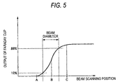
FIGS. 4A to 4C are typical views showing the relationship between the electron beam 100 incident on the Faraday cup 140 and the wires 120 and 130. For simplification, a wire 120 is taken as an example here. As shown in FIG. 4A, if the electron beam 100 is totally applied over the wire 120, the electron beam 100 is obstructed by the wire 120, and does not enter the Faraday cup. This state is defined as state A. Next, if the electron beam 100 is applied near an edge of the wire 120, a partial electron beam 101.passes by the wire 120 to enter the Faraday cup, while a remaining electron beam 102 is scattered by the wire 120 to produce scattered electrons 103. This state is defined as state B. Moreover, when the electron beam 100 is not applied to the wire 120, but totally passes by, all the electron beam 100 is incident on the Faraday cup 140. This state is defined as state C.
FIG. 5 is a graph showing an output waveform of the Faraday cup 140 when one of the wires 120 and 130 is continuously scanned using the electron beam 100. In the graph of FIG. 5, the axis of abscissas is the beam scan position, and the axis of ordinates is the output of the Faraday cup 140, in which “A”, “B” and “C” on the axis of abscissas correspond to the states as shown in FIGS. 4A to 4C. As shown in FIG. 5, the output of the Faraday cup 140 rapidly rises from state A to state C. In the adjustment, the beam profile is assumed to be Gaussian, and the width between the beam position at which the output of the Faraday cup 140 is 12% and the beam position at which it is 88% is defined as a beam diameter. The adjustment is made in each of the x and y directions to minimize the beam diameter and make the beam diameter almost equal to produce an almost circular spot electron beam with high precision.
However, with the above method, when the coarse adjustment using the latex balls is insufficient, it is required to repeat the adjustment many times to continue the operation, until an excellent beam diameter is obtained, which takes a quite enormous time. Also, this adjustment needs some experience, and is not treated simply.
With the cross wire method, though two wires are employed to measure the beam diameters in the x and y directions, the measurement height is different in the adjustment in the x and y directions by an amount of wire width, because the wire has a width, as shown in FIG. 3. Accordingly, the correct height position of the cross wire is not accurately measured, resulting in an error in the measurement precision.
Also, in the state B, the partial electron beam 100 is scattered as the scattered electrons 103, but part of scattered electrons 103 are scattered by the wire 120 to enter the Faraday cup 140, as shown in FIG. 4B. Accordingly, an output curve of the Faraday cup as shown in FIG. 5 is raised by part of scattered electrons and does not represent the beam profile accurately. Accordingly, it is difficult to make the measurement at high precision.
Also, the wires 120 and 130 are partially varied in the shape, the height in the z axis direction being possibly different depending on the position, whereby the measurement precision is degraded due to this height error.
SUMMARY OF THE INVENTION
This invention has been achieved in the light of the above-mentioned problems, and it is an object of the invention to solve the difficulty of making the measurement with high precision with the cross wire method.
To achieve the above object, according to one aspect of the invention, there is provided a beam adjusting method comprising: applying a beam onto a beam adjusting sample having a flat surface being like a plate and having two edges orthogonal to each other, and a step of detecting an amount of the beam passing through the beam adjusting sample, wherein the beam vertically scans the two edges.
According to another aspect of the invention, there is provided a beam adjusting sample having a flat surface being like a plate and has two edges orthogonal to each other.
According to still another aspect of the invention, there is provided a beam adjusting device comprising a stage for laying a beam adjusting sample having a flat surface being like a plate and having two edges orthogonal to each other, a beam generator for applying a beam onto the beam adjusting sample, a secondary electron detector for detecting a secondary electron generated by applying the beam, a position detector for detecting the position of the beam adjusting sample, and a beam detector disposed under the stage, wherein the beam detector detects an amount of electron beam passing through the beam adjusting sample.
BRIEF DESCRIPTION OF THE DRAWINGS
These and other objects and advantages of this invention will become more fully apparent from the following detailed description taken with the accompanying drawings in which:
FIG. 1 is a view for explaining the coarse control of electron beam.
FIG. 2 is a view for explaining a method for measuring a beam diameter of electron beam using a cross wire method.
FIG. 3 is a view showing the positional relation between the cross wires.
FIGS. 4A to 4C are typical views showing the relationship between electron beam incident on the Faraday cup and the wire.
FIG. 5 is a graph showing the relationship between the beam scan position and the output of the Faraday cup.
FIG. 6 is a cross-sectional view showing a beam adjusting device according to an embodiment of the invention.
FIG. 7 is a perspective view showing a sample laid on the Faraday cup.
FIGS. 8A and 8B are cross-sectional views taken along the line VIII-VIII in FIG. 7.
FIGS. 9A and 9B are views showing a scan pattern of electron beam applied to the sample.
FIGS. 10A to 10C are typical views showing the relationship between an electron beam applied to the sample and an electron beam passing through a through hole.
FIG. 11 is a graph showing the relationship between the beam scan position and the output of the Faraday cup.
FIG. 12 is a flowchart showing a beam adjusting method according to the embodiment.
FIGS. 13A to 13C are views showing one variation of the embodiment.
FIGS. 14A to 14C are views showing another variation of the embodiment.
DETAILED DESCRIPTION OF THE PREFERRED EMBODIMENTS
Referring to FIGS. 6 to 12, a beam adjusting sample, a beam adjusting method and a beam adjusting device according to an embodiment of the present invention.
FIG. 6 is a cross-sectional view showing the beam adjusting device according to the embodiment of the invention. The beam adjusting device 1 of this embodiment comprises a vacuum container 3 for laying a sample 50 thereon, and a cylindrical electron beam radiating portion 2 for radiating the electron beam toward the sample 50, in which the cylindrical electron beam radiating portion 2 is mounted on the vacuum container 3.
The electron beam radiating portion 2 comprises an electron beam source 10 for generating the electron beam, an alignment coil 20, a focusing lens 21, a stigma coil 22, a deflecting coil 23, and an objective lens 24. These coils or lenses 20 to 24 include the cylindrical coils, through which the generated electron beam is passed.
The electron beam source 10 comprises a cathode 11 disposed on the axial line of the electron beam radiating portion 2, a Wehnelt 12 for covering the side face of the cathode 11, with a certain distance off the side face, and an anode 13 disposed on the side of the vacuum container 3 rather than the cathode 11. If a predetermined voltage is applied to the cathode 11, the Wehnelt 12 and the anode 13, electrons fly out of the cathode 11. Flying out electrons are axially aligned to move to the vacuum container 3.
The focusing lens 21 focuses the electron beam axially aligned by the alignment coil 20 and converges it into the electron beam having a predetermined diameter.
The stigma coil 22 adjusts the astigmatism of the electron beam passing through the coil so that the electron beam may be symmetrical around the axis. When the astigmatism takes place by changing the parameters of various kinds of lenses or coils, the stigma coil 22 is adjusted to correct the astigmatism. This adjusting method will be described later.
The deflecting coil 23 deflects the electron beam in the x and y directions perpendicular to an incident direction of the electron beam. As a voltage applied to the deflecting coil 23 is varied, the electron beam passing through the deflecting coil 23 is changed in its travel direction under the influence of a magnetic field generated by the coil. A continuously changing alternating current of rectangular or triangular wave is applied to this deflecting coil 23 to continuously change a direction of the electron beam in accordance with a pattern of applied alternating current.
The objective lens 24 converges the electron beam and adjusts the focal point along the incident direction (z direction) of the electron beam. The objective lens 24 is adjusted to focus the electron beam on the sample 50 laid within the vacuum container 3.
The vacuum container 3 is evacuated by an exhaust tube and a vacuum pump, not shown. Inside the vacuum container 3, a stage 33 and a Faraday cup 34 are disposed along the incident direction of the electron beam. The stage 33 lays the Faraday cup 34 or the sample 50 on its upper face to be movable in the x, y or z direction, and provides a reference plane for the measurement.
The Faraday cup 34 and the sample 50 laid on the Faraday cup 34 are fixed on the stage 33. The Faraday cup 34 is a beam detector for detecting the electron beam passing through the sample 50 and converting it into an electrical signal in accordance with an amount of received beam. The Faraday cup 34 is constituted to make the sample 50 parallel to the stage 33.
A laser radiating unit 30 and a laser receiving unit 31 for measuring the upper surface position of the sample are mounted on an upper surface of the vacuum container 3. The laser radiating unit 30 radiates a laser beam to the upper face of the sample 50 laid on the Faraday cup 34. The laser receiving unit 31 receives the laser beam reflected from the sample 50 to detect the height position of the sample 50.
Also, a secondary electron detector 32 is disposed in the vacuum container 3. The secondary electron detector 32 captures secondary electrons emitted from each point of the sample 50 irradiated by the laser beam. The emission amount of secondary electrons may be increased or decreased depending on the shape of the sample surface such as the inclination or edges of the sample surface. The captured secondary electrons are amplified and displayed two-dimensionally for each captured point, whereby an image of the surface shape of the sample 50 is acquired.
FIG. 7 is a perspective view showing the sample 50 laid on the Faraday cup 34, and FIGS. 8A and 8B are cross-sectional views taken along the line VIII-VIII in FIG. 7. The sample 50 is a plate-like silicon wafer having a flat surface, with a through hole 51 opened near the central part of the silicon wafer. Also, a microstructure 53 having a known size and including latex balls 53 a is attached on the surface of the sample 50 near the through hole 51. The sample 50 has preferably a uniformly flat surface without regard to the position to increase the measurement precision, or conversely, a member having the flat surface may be substituted for the silicon wafer.
Herein, a film of an element having a high electron stopping power is preferably coated on the surface of the microstructure 53 of the sample 50. Since the surface of the sample 50 is irradiated repeatedly by the electron beam, the applied electron beam is embedded from the surface into the sample 50 to charge up the surface, possibly having an adverse influence on the emission amount of secondary electrons. Therefore, to prevent the charge-up of the surface, a film of an element W, Ta, Mo or Pt of high atomic number having a high electron stopping power is preferably coated on the surface. The thickness of this film is preferably 100 nm or more.
The through hole 51 has a square or rectangle shape as seen from above, the adjacent edges 52 being orthogonal. The inner side face of the through hole 51 is formed at right angles to the surface of the sample 50 as shown in FIGS. 8A and 8B. Also, the angle of the inner side face of the through hole 51 made to the surface of the sample 50 may be less than 90°, as shown in FIGS. 9A and 9B.
In this embodiment, the edges 52 of the through hole 51 in this sample 50 are employed instead of two wires with the cross wire method. FIGS. 9A and 9B are views showing the patterns of scanning the electron beam applied to the sample 50. In this embodiment, the electron beam is radiated from the surface of the sample 50 vertically across an edge 52 into the through hole 51, and then vertically across the adjacent edge 52 to the sample 50 again.
In FIG. 9A, the electron beam has its radiation direction rotated by 90° over the through hole 51, and then is moved toward the adjacent edge 52. Also, in FIG. 9B, the electron beam is radiated to draw a circular locus around a predetermined center of rotation. In FIG. 9B, the electron beam has its locus crossing vertically the edges 52.
FIGS. 10A to 10C are typical views showing the relationship between the electron beam radiated to the sample 50 and the electron beam passing through the through hole 51. First of all, the electron beam 200 is radiated toward the surface of the sample 50. At this time, the electron beam 200 is impeded on the surface of the sample 50, and does not enter the Faraday cup 34 placed under it.
Then, if the electron beam 200 is radiated near the edges 52 of the through hole 51, a partial electron beam 201 passes by the edges 52 to be incident upon the Faraday cup 34, and a remaining electron beam 202 is impeded on the surface of the sample 50 near the edges 52, and scattered as scattered electrons 203. Since the scattered electrons 203 are scattered on the surface of the sample 50, almost no scattered electrons pass through the through hole 51 to enter the Faraday cup 34. This state is defined as state E.
Moreover, if the electron beam is moved to the position where it totally passes through the through hole 52, the Faraday cup 34 receives all the electron beam 200. This state is defined as state F. the above states D to F are the same, whether the electron beam 200 is moved in the x direction or the y direction.
FIG. 11 is a graph showing an output of the Faraday cup when the surface of the sample 50 is scanned along a scan path as shown in FIG. 9A, using the electron beam 200. In the graph, the axis of abscissas is the beam scan position and the axis of ordinates is the output of the Faraday cup 140, in which “D”, “E” and “F” indicated on the axis of abscissas correspond to the states as shown in FIGS. 10A to 10C, respectively.
In the state D where the electron beam 200 is radiated on the surface of the sample 50, the amount of electron beam incident on the Faraday cup 34 is zero. If the electron beam 200 is moved in the x direction to the position (state E) on the edges 52 of the through hole 51, the amount of electron beam passing through the through hole 51 and entering the Faraday cup 34 is increased. And at the position (state F) where the electron beam 200 totally passes through the through hole 51, the incident amount of electron beam is not increased, and kept at a certain value.
If the movement direction of the electron beam 200 is changed to the y direction to move the electron beam 200 via the edges 52 on the surface of the sample 50 again, the output of the Faraday cup 34 is decreased to zero as shown to the right in the graph of FIG. 11.
In the adjustment of this embodiment, the beam profile is assumed as Gaussian, and the beam diameter is defined as the width between the beam position at which the output of the Faraday cup 34 is 12% and the beam position at which it is 88%. And the adjustment is made such that the beam diameter is minimized and almost equivalent in the x and y directions, whereby an almost circular spot electron beam is produced at high precision. Herein, to assure that the beam diameter in the x and y directions is almost equivalent, it is required that the output curve of the Faraday cup in FIG. 11 is symmetrical in the degree of change.
Referring to FIG. 12, the flow of a beam adjusting method of this embodiment will be detailed below in consideration of the above description.
Firstly, the Faraday cup 34 and the sample 50 are laid on the stage 33 within the vacuum container. At this time, the height position of the stage 33 is roughly adjusted to be flush with the recording (drawing) plane. At this time, the surface height of the sample 50 is measured accurately using the laser radiating unit 30 and the laser receiving unit 31 for measurement of the upper face position (step S1).
Then, the electron beam 200 is radiated to the microstructure 53 including latex balls 53 a attached on the sample 50 to make the coarse adjustment by focusing it in the z axis direction based on a produced image of secondary electrons (step S2).
Thereafter, the stage 33 is moved in the x and y directions, so that the electron beam 200 may be positioned near the through hole 51 of the sample 50. And the electron beam is scanned and radiated from the surface of the sample 50 via the edge 52 into the through hole 51. At this time, the electron beam is moved to vertically traverse the edge 52 (step S3). If the electron beam 200 arrives near the center of the through hole 51 and gets to the position at which it totally passes through the sample 50, the scan direction of the electron beam 200 is rotated by 90° (step S4). And the electron beam is scanned and radiated in the y direction onto the surface of the sample 50 through the through hole 51 via the adjacent edge 52 near the previously passed edge (step S5). The operation from step S3 to step S5 may be ended at a time or repeated on the same path two or more times.
Thereafter, the output of the Faraday cup is confirmed to check whether or not the adjustment is ended. If the adjustment is less sufficient, the stigma coil 22 is adjusted to change the beam parameters, and the operation returns to step S3. If there is no problem, the measurement is ended.
In brief, the beam adjusting method of this embodiment includes a step of radiating electron beam to the sample 50 for beam adjustment having a flat surface of plate shape and formed with the through hole 52 opened in the thickness direction, and a step of detecting the amount of beam penetrating the sample 50 for beam adjustment through the through hole 52, in which the electron beam is radiated by changing the scan direction over the through hole 52.
According to this embodiment, the single sample 50 can be employed to make the coarse adjustment of beam in the z direction and the adjustment of beam diameter in the x and y directions. Accordingly, the operation for adjusting the beam is simplified and the time for beam adjustment is shortened.
Also, the beam diameter adjustment in the x and y directions is made by beam scan once. Since the reference plane in the x and y directions is the same surface of the sample 50, there is no height error when the adjustment is made in the x and y directions.
The sample 50 is made from a silicon wafer, with almost no height error. Moreover, since the height position of the surface of the sample 50 is accurately measured using the laser radiating unit 30 and the laser receiving unit 31, the correct beam measurement position is grasped.
Also, a film made of an element having high electron stopping power is coated on the microstructure to prevent the charge-up and make an error in the emission amount of secondary electrons smaller. Also, this film reduces a damage of the sample 50 caused by the electron charge-up, whereby the sample can have the higher durability.
The beam measuring device, the beam measuring method and the beam measuring sample of this embodiment are applicable to a scan-type electron microscope, as well as a recording apparatus for recording the information on the disk using the electron beam. The beam measuring device, the beam measuring method and the beam measuring sample of this embodiment are suitable for the recording apparatus for high density requiring the formation of minute patterns, since the electron beam is adjusted at high precision.
In the above embodiment, the sample 50 has the through hole near the central part. Besides, the electron beam may transverse vertically two orthogonal ends.
FIG. 13A is a perspective view showing a sample 60 laid on the Faraday cup 34 as one variation of the sample 50, and FIGS. 13B and 13C are views showing the scan patterns of the electron beam. The sample 60 is a silicone wafer having a flat surface and shaped like a plate. A microstructure 63 of known size including latex balls 63 a is attached on the surface of the sample 60. The sample 60 has preferably a uniformly flat surface over the entire area to increase the measurement precision, or conversely a member having a flat surface may be used instead of the silicon wafer.
Herein, a film of an element W, Ta, Mo or Pt of high atomic number having a high electron stopping power is preferably coated on the surface of the microstructure 63 of the sample 60 to prevent the charge-up. The thickness of this film is preferably 100 nm or more.
The sample 60 has two adjacent edges 61 and 62 orthogonal as seen from above. The edges 61 and 62 may be perpendicular to the surface as in FIG. 8A, or may make an angle of less than 90° as in FIG. 8B.
In this variation, the electron beam is radiated from the outside of the sample 60 vertically across an edge 61 onto the surface of the sample 60, and then vertically across the adjacent edge onto the outside of the sample 60 again.
In FIG. 13B, the electron beam is rotated 90° in the radiation direction on the sample 60, and then moves to the adjacent edge. Also, in FIG. 13C, the electron beam is radiated to draw a circular locus around a predetermined center of rotation. In FIG. 13C, the electron beam has its locus crossing vertically the edges 61 and 62. In this variation, the Faraday cup 34 receives the electron beam not impeded by the sample 60 and passing through the sample 60 and measures the amount of beam. The sample 60 as constituted in this variation can provide the same effect as the sample 50.
FIG. 14A is a perspective view showing a sample 70 laid on the Faraday cup 34 as another variation of the sample 50, and FIGS. 14B and 14C are views showing the scan patterns of the electron beam. The sample 70 is a silicone wafer having a flat surface and shaped like a plate. A microstructure 75 of known size including latex balls 75 a is attached on the surface of the sample 70. The sample 70 has preferably a uniformly flat surface over the entire area to increase the measurement precision, or conversely a member having a flat surface may be used instead of the silicon wafer.
Herein, a film of an element W, Ta, Mo or Pt of high atomic number having a high electron stopping power is preferably coated on the surface of the microstructure 75 of the sample 70 to prevent the charge-up. The thickness of this film is preferably 100 nm or more.
The sample 70 has a corner portion crossed by two adjacent edges 71 and 72 cut away, and provided with two edges 73 and 74 orthogonal to each other. The edges 73 and 74 may be at right angles to the surface as in FIG. 8A, or may make an angle of less than 90° as in FIG. 8B.
In this variation, the electron beam is radiated from the surface of the sample 70 vertically across an edge 73 to the outside of the sample 70, and then vertically across an adjacent edge 74 onto the surface of the sample 70 again.
In FIG. 14B, the electron beam is rotated 90° in the radiation direction outside the sample 70, and then moves to the adjacent edge. Also, in FIG. 14C, the electron beam is radiated to draw a circular locus around a predetermined center of rotation. In FIG. 14C, the electron beam has its locus crossing vertically the edges 73 and 74. In this variation, the Faraday cup 34 receives the electron beam not impeded by the sample 70 and passing through the sample 70 and measures the amount of beam. The sample 70 as constituted in this variation can provide the same effect as the samples 50 and 60.
The foregoing description of the preferred embodiments of the invention has been presented for purposes of illustration and description. It is not intended to be exhaustive or to limit the invention to the precise form disclosed, and modifications and variations are possible in light of the above teachings or may be acquired from practice of the invention. The embodiments were chosen and described in order to explain the principles of the invention and its practical application to enable one skilled in the art to utilize the invention in various embodiments and with various modifications as are suited to the particular use contemplated. It is intended that the scope of the invention be defined by the claims appended hereto, and their equivalents.

Claims (12)

1. A beam adjusting sample including a flat surface being like a plate and having at least two edges in which adjacent edges are orthogonal to each other as viewed from above the beam adjusting sample,
wherein a microstructure including latex balls is attached on the surface of the beam adjusting sample, and
wherein a film of an element having a high electron stopping power is coated on a surface of the microstructure, wherein the thickness of the film is 100 nm or more.
2. The beam adjusting sample according to claim 1, wherein the beam adjusting sample is defined by the two edges, and has a through hole penetrating in the thickness direction.
3. The beam adjusting sample according to claim 1, wherein the two edges are two edges at the beam adjusting sample end.
4. The beam adjusting sample according to claim 1 wherein the attached microstructure is located near the through hole.
5. The beam adjusting sample according to claim 1 wherein the film is of one element W, Ta, Mo, Pt of high atomic number.
6. The beam adjusting sample according to claim 1 wherein the through hole is located near a central part of the sample.
7. The beam adjusting sample according to claim 2, wherein an inner side face of the through hole is formed at an angle smaller than or equal to 90 degrees to the surface of the beam adjusting sample.
8. A beam adjusting device comprising: stage for laying a beam adjusting sample as claimed in claim 1;
a beam generator for applying a beam onto the beam adjusting sample;
a secondary electron detector for detecting a secondary electron generated by applying the beam;
a position detector for detecting the position of the beam adjusting sample; and
a beam detector disposed under the stage, wherein the beam detector detects an amount of electron beam passing through the beam adjusting sample.
9. The beam adjusting device according to claim 8, wherein the beam adjusting sample is defined by the two edges, and has a through hole penetrating in a thickness direction, and the beam generator applies the electron beam to have a scan direction changed over the through hole.
10. The beam adjusting device according to claim 8, wherein the two edges of the beam adjusting sample are two edges at the end of the beam adjusting sample, and the beam generator applies the beam to have the scan direction changed over the beam adjusting sample or outside the beam adjusting sample.
11. The beam adjusting device according to claim 8, wherein the beam generator applies the beam onto a microstructure placed on the surface of the beam adjusting sample.
12. The beam adjusting device according to claim 11, wherein a film of an element having a high electron stopping power is coated on the surface of the microstructure.
US10/679,416 2002-10-11 2003-10-07 Beam adjusting sample, beam adjusting method and beam adjusting device Expired - Lifetime US7276692B2 (en)

Applications Claiming Priority (2)

Application Number Priority Date Filing Date Title
JPP2002-298359 2002-10-11
JP2002298359A JP3960544B2 (en) 2002-10-11 2002-10-11 Beam adjusting specimen, beam adjusting method and beam adjusting apparatus

Publications (2)

Publication Number Publication Date
US20040069952A1 US20040069952A1 (en) 2004-04-15
US7276692B2 true US7276692B2 (en) 2007-10-02

Family

ID=32025578

Family Applications (1)

Application Number Title Priority Date Filing Date
US10/679,416 Expired - Lifetime US7276692B2 (en) 2002-10-11 2003-10-07 Beam adjusting sample, beam adjusting method and beam adjusting device

Country Status (3)

Country Link
US (1) US7276692B2 (en)
EP (1) EP1408532A3 (en)
JP (1) JP3960544B2 (en)

Cited By (2)

* Cited by examiner, † Cited by third party
Publication number Priority date Publication date Assignee Title
US20080006781A1 (en) * 2004-06-21 2008-01-10 Pioneer Corporation Electron Beam Drawing Apparatus
US20120217392A1 (en) * 2011-02-28 2012-08-30 Tsutomu Murakawa Pattern-height measuring apparatus and pattern-height measuring method

Families Citing this family (5)

* Cited by examiner, † Cited by third party
Publication number Priority date Publication date Assignee Title
CN1929070B (en) * 2005-09-09 2010-08-11 鸿富锦精密工业(深圳)有限公司 Electron source and surface light source employing same
WO2012084363A1 (en) * 2010-12-20 2012-06-28 Asml Netherlands B.V. Method and system for monitoring the integrity of an article, and euv optical apparatus incorporating the same
ES2844324T3 (en) * 2011-11-07 2021-07-21 Beckman Coulter Inc Robotic arm
JP7054995B2 (en) * 2017-07-12 2022-04-15 オルガノ株式会社 Evaluation method of ultrapure water, evaluation method of membrane module for ultrapure water production, and evaluation method of ion exchange resin for ultrapure water production
JP7160857B2 (en) * 2020-05-20 2022-10-25 日本電子株式会社 Beam adjustment method and three-dimensional additive manufacturing apparatus

Citations (10)

* Cited by examiner, † Cited by third party
Publication number Priority date Publication date Assignee Title
US4370554A (en) * 1979-09-27 1983-01-25 International Business Machines Corporation Alignment system for particle beam lithography
DE3228813A1 (en) 1981-11-02 1983-05-26 Jenoptik Jena Gmbh, Ddr 6900 Jena Method and arrangement for determining structural edges in electron beam apparatuses
US4513203A (en) * 1981-05-30 1985-04-23 International Business Machines Corporation Mask and system for mutually aligning objects in ray exposure systems
US4912313A (en) * 1987-11-27 1990-03-27 Hitachi Ltd. Method of measuring surface topography by using scanning electron microscope, and apparatus therefor
JPH05159735A (en) 1991-12-03 1993-06-25 Pioneer Electron Corp Electron beam projecting device
US5430292A (en) 1991-06-10 1995-07-04 Fujitsu Limited Pattern inspection apparatus and electron beam apparatus
JPH09190792A (en) 1996-01-11 1997-07-22 Jeol Ltd Method for adjusting focus of focusing beam
US6243348B1 (en) * 1998-06-05 2001-06-05 Massachusetts Institute Of Technology Very-high-density memory device utilizing a scintillating data-storage medium
WO2002043104A2 (en) 2000-11-22 2002-05-30 Varian Semiconductor Equipment Associates, Inc. Hybrid scanning system and methods for ion implantation
US6426501B1 (en) 1998-05-27 2002-07-30 Jeol Ltd. Defect-review SEM, reference sample for adjustment thereof, method for adjustment thereof, and method of inspecting contact holes

Patent Citations (10)

* Cited by examiner, † Cited by third party
Publication number Priority date Publication date Assignee Title
US4370554A (en) * 1979-09-27 1983-01-25 International Business Machines Corporation Alignment system for particle beam lithography
US4513203A (en) * 1981-05-30 1985-04-23 International Business Machines Corporation Mask and system for mutually aligning objects in ray exposure systems
DE3228813A1 (en) 1981-11-02 1983-05-26 Jenoptik Jena Gmbh, Ddr 6900 Jena Method and arrangement for determining structural edges in electron beam apparatuses
US4912313A (en) * 1987-11-27 1990-03-27 Hitachi Ltd. Method of measuring surface topography by using scanning electron microscope, and apparatus therefor
US5430292A (en) 1991-06-10 1995-07-04 Fujitsu Limited Pattern inspection apparatus and electron beam apparatus
JPH05159735A (en) 1991-12-03 1993-06-25 Pioneer Electron Corp Electron beam projecting device
JPH09190792A (en) 1996-01-11 1997-07-22 Jeol Ltd Method for adjusting focus of focusing beam
US6426501B1 (en) 1998-05-27 2002-07-30 Jeol Ltd. Defect-review SEM, reference sample for adjustment thereof, method for adjustment thereof, and method of inspecting contact holes
US6243348B1 (en) * 1998-06-05 2001-06-05 Massachusetts Institute Of Technology Very-high-density memory device utilizing a scintillating data-storage medium
WO2002043104A2 (en) 2000-11-22 2002-05-30 Varian Semiconductor Equipment Associates, Inc. Hybrid scanning system and methods for ion implantation

Non-Patent Citations (1)

* Cited by examiner, † Cited by third party
Title
Hitoshi Nishimura: Japanese Patent Office Examiner-Notification of Reasons for Refusal for JP Patent Application No. 2002-298359: Art 29-1, Art. 29-2, Art 38.

Cited By (4)

* Cited by examiner, † Cited by third party
Publication number Priority date Publication date Assignee Title
US20080006781A1 (en) * 2004-06-21 2008-01-10 Pioneer Corporation Electron Beam Drawing Apparatus
US7679071B2 (en) * 2004-06-21 2010-03-16 Pioneer Corporation Electron beam drawing apparatus
US20120217392A1 (en) * 2011-02-28 2012-08-30 Tsutomu Murakawa Pattern-height measuring apparatus and pattern-height measuring method
US8604431B2 (en) * 2011-02-28 2013-12-10 Advantest Corp. Pattern-height measuring apparatus and pattern-height measuring method

Also Published As

Publication number Publication date
EP1408532A2 (en) 2004-04-14
JP2004132863A (en) 2004-04-30
US20040069952A1 (en) 2004-04-15
EP1408532A3 (en) 2005-11-09
JP3960544B2 (en) 2007-08-15

Similar Documents

Publication Publication Date Title
US7312449B2 (en) Electron beam system and method of manufacturing devices using the system
US7005641B2 (en) Electron beam apparatus and a device manufacturing method by using said electron beam apparatus
US7378668B2 (en) Method and apparatus for applying charged particle beam
JP3441955B2 (en) Projection type charged particle microscope and substrate inspection system
US20220246388A1 (en) Multiple particle beam microscope and associated method with an improved focus setting taking into account an image plane tilt
US8067733B2 (en) Scanning electron microscope having a monochromator
US7705298B2 (en) System and method to determine focus parameters during an electron beam inspection
US7282711B2 (en) Multiple electron beam device
US7276692B2 (en) Beam adjusting sample, beam adjusting method and beam adjusting device
JP2003157790A (en) Micro ruggedness value measurement device and scanning electron microscope
EP0780878B1 (en) Scanning electron microscope
JPH0458104A (en) Electron beam size measuring instrument
TW472298B (en) Electron beam exposure apparatus, adjusting method, and block mask for adjustment
JPWO2002075246A1 (en) Pattern dimension measurement method
KR20160020598A (en) Apparatus and method for controlling Charged Particle Beam in Charged Particle Microscope
JP2001210689A (en) Method and apparatus for electron beam inspection
JP7182003B2 (en) charged particle beam system
KR101618693B1 (en) Method for controlling scanning profile in Charged Particle Microscope and apparatus using thereof
JP4212181B2 (en) Semiconductor exposure method and exposure apparatus
JPH09293474A (en) Sample image measuring apparatus
JP4627731B2 (en) Height detection apparatus and height detection method used for charged particle beam apparatus
JP2007019193A (en) Charged particle beam equipment, method for regulating lens power, and process for fabricating device
JP2018067605A (en) Multi-beam focus control method and multi-beam focus measuring method
CN1497656A (en) Beam regulating sample, beam regulating method and beam regulating device

Legal Events

Date Code Title Description
AS Assignment

Owner name: PIONEER CORPORATION, JAPAN

Free format text: ASSIGNMENT OF ASSIGNORS INTEREST;ASSIGNORS:KATSUMURA, MASAHIRO;KOJIMA, YOSHIAKI;WADA, YASUMITSU;AND OTHERS;REEL/FRAME:014590/0275

Effective date: 20030925

STCF Information on status: patent grant

Free format text: PATENTED CASE

FEPP Fee payment procedure

Free format text: PAYOR NUMBER ASSIGNED (ORIGINAL EVENT CODE: ASPN); ENTITY STATUS OF PATENT OWNER: LARGE ENTITY

FPAY Fee payment

Year of fee payment: 4

AS Assignment

Owner name: NUFLARE TECHNOLOGY, INC., JAPAN

Free format text: ASSIGNMENT OF ASSIGNORS INTEREST;ASSIGNOR:PIONEER CORPORATION;REEL/FRAME:028116/0384

Effective date: 20120227

FPAY Fee payment

Year of fee payment: 8

MAFP Maintenance fee payment

Free format text: PAYMENT OF MAINTENANCE FEE, 12TH YEAR, LARGE ENTITY (ORIGINAL EVENT CODE: M1553); ENTITY STATUS OF PATENT OWNER: LARGE ENTITY

Year of fee payment: 12