US7276318B2 - Electrophotographic photosensitive member, and electrophotographic apparatus and process cartridge which make use of the same - Google Patents

Electrophotographic photosensitive member, and electrophotographic apparatus and process cartridge which make use of the same Download PDF

Info

Publication number
US7276318B2
US7276318B2 US10/981,564 US98156404A US7276318B2 US 7276318 B2 US7276318 B2 US 7276318B2 US 98156404 A US98156404 A US 98156404A US 7276318 B2 US7276318 B2 US 7276318B2
Authority
US
United States
Prior art keywords
group
photosensitive member
atom
electrophotographic photosensitive
semiconductor laser
Prior art date
Legal status (The legal status is an assumption and is not a legal conclusion. Google has not performed a legal analysis and makes no representation as to the accuracy of the status listed.)
Expired - Fee Related, expires
Application number
US10/981,564
Other versions
US20050181292A1 (en
Inventor
Atsushi Fujii
Masato Tanaka
Current Assignee (The listed assignees may be inaccurate. Google has not performed a legal analysis and makes no representation or warranty as to the accuracy of the list.)
Canon Inc
Original Assignee
Canon Inc
Priority date (The priority date is an assumption and is not a legal conclusion. Google has not performed a legal analysis and makes no representation as to the accuracy of the date listed.)
Filing date
Publication date
Application filed by Canon Inc filed Critical Canon Inc
Assigned to CANON KABUSHIKI KAISHA reassignment CANON KABUSHIKI KAISHA ASSIGNMENT OF ASSIGNORS INTEREST (SEE DOCUMENT FOR DETAILS). Assignors: FUJII, ATSUSHI, TANAKA, MASATO
Publication of US20050181292A1 publication Critical patent/US20050181292A1/en
Priority to US11/687,163 priority Critical patent/US7517626B2/en
Application granted granted Critical
Publication of US7276318B2 publication Critical patent/US7276318B2/en
Expired - Fee Related legal-status Critical Current
Adjusted expiration legal-status Critical

Links

Images

Classifications

    • GPHYSICS
    • G03PHOTOGRAPHY; CINEMATOGRAPHY; ANALOGOUS TECHNIQUES USING WAVES OTHER THAN OPTICAL WAVES; ELECTROGRAPHY; HOLOGRAPHY
    • G03GELECTROGRAPHY; ELECTROPHOTOGRAPHY; MAGNETOGRAPHY
    • G03G5/00Recording members for original recording by exposure, e.g. to light, to heat, to electrons; Manufacture thereof; Selection of materials therefor
    • G03G5/02Charge-receiving layers
    • G03G5/04Photoconductive layers; Charge-generation layers or charge-transporting layers; Additives therefor; Binders therefor
    • G03G5/06Photoconductive layers; Charge-generation layers or charge-transporting layers; Additives therefor; Binders therefor characterised by the photoconductive material being organic
    • G03G5/0664Dyes
    • G03G5/0675Azo dyes
    • G03G5/0679Disazo dyes
    • G03G5/0681Disazo dyes containing hetero rings in the part of the molecule between the azo-groups
    • CCHEMISTRY; METALLURGY
    • C07ORGANIC CHEMISTRY
    • C07CACYCLIC OR CARBOCYCLIC COMPOUNDS
    • C07C229/00Compounds containing amino and carboxyl groups bound to the same carbon skeleton
    • C07C229/02Compounds containing amino and carboxyl groups bound to the same carbon skeleton having amino and carboxyl groups bound to acyclic carbon atoms of the same carbon skeleton
    • C07C229/04Compounds containing amino and carboxyl groups bound to the same carbon skeleton having amino and carboxyl groups bound to acyclic carbon atoms of the same carbon skeleton the carbon skeleton being acyclic and saturated
    • C07C229/06Compounds containing amino and carboxyl groups bound to the same carbon skeleton having amino and carboxyl groups bound to acyclic carbon atoms of the same carbon skeleton the carbon skeleton being acyclic and saturated having only one amino and one carboxyl group bound to the carbon skeleton
    • C07C229/18Compounds containing amino and carboxyl groups bound to the same carbon skeleton having amino and carboxyl groups bound to acyclic carbon atoms of the same carbon skeleton the carbon skeleton being acyclic and saturated having only one amino and one carboxyl group bound to the carbon skeleton the nitrogen atom of the amino group being further bound to carbon atoms of six-membered aromatic rings
    • GPHYSICS
    • G03PHOTOGRAPHY; CINEMATOGRAPHY; ANALOGOUS TECHNIQUES USING WAVES OTHER THAN OPTICAL WAVES; ELECTROGRAPHY; HOLOGRAPHY
    • G03GELECTROGRAPHY; ELECTROPHOTOGRAPHY; MAGNETOGRAPHY
    • G03G5/00Recording members for original recording by exposure, e.g. to light, to heat, to electrons; Manufacture thereof; Selection of materials therefor
    • G03G5/02Charge-receiving layers
    • G03G5/04Photoconductive layers; Charge-generation layers or charge-transporting layers; Additives therefor; Binders therefor
    • G03G5/05Organic bonding materials; Methods for coating a substrate with a photoconductive layer; Inert supplements for use in photoconductive layers
    • G03G5/0528Macromolecular bonding materials
    • G03G5/0557Macromolecular bonding materials obtained otherwise than by reactions only involving carbon-to-carbon unsatured bonds
    • G03G5/0575Other polycondensates comprising nitrogen atoms with or without oxygen atoms in the main chain
    • GPHYSICS
    • G03PHOTOGRAPHY; CINEMATOGRAPHY; ANALOGOUS TECHNIQUES USING WAVES OTHER THAN OPTICAL WAVES; ELECTROGRAPHY; HOLOGRAPHY
    • G03GELECTROGRAPHY; ELECTROPHOTOGRAPHY; MAGNETOGRAPHY
    • G03G5/00Recording members for original recording by exposure, e.g. to light, to heat, to electrons; Manufacture thereof; Selection of materials therefor
    • G03G5/02Charge-receiving layers
    • G03G5/04Photoconductive layers; Charge-generation layers or charge-transporting layers; Additives therefor; Binders therefor
    • G03G5/06Photoconductive layers; Charge-generation layers or charge-transporting layers; Additives therefor; Binders therefor characterised by the photoconductive material being organic
    • G03G5/0664Dyes
    • G03G5/0675Azo dyes
    • G03G5/0679Disazo dyes
    • G03G5/0683Disazo dyes containing polymethine or anthraquinone groups

Definitions

  • This invention relates to an image forming apparatus (electrophotographic apparatus) such as a copying machine, a printer, a facsimile machine or a platemaking system, which employs an electrophotographic process.
  • an image forming apparatus such as a copying machine, a printer, a facsimile machine or a platemaking system, which employs an electrophotographic process.
  • the exposure process that forms an electrostatic latent image on the surface of an electrophotographic photosensitive member is positioned on the upstream side in the electrophotographic process, and is the basis of image formation. Accordingly, this process is considered to be an especially important process in order to achieve high image quality of electrophotographic images. Then, making beam spot diameter small in the exposure process enables achievement of ultrahigh resolution, and is a very effective means for the achievement of ultrahigh image quality.
  • Near infrared region semiconductor lasers having conventionally been used have lasing wavelengths of about 650 to 780 nm, and have spot diameter of about 100 ⁇ m. Its limit has been about 50 to 80 ⁇ m whatever improvements are made on various optical members in order to make the beam spot diameter small. Also, even if improvements on various optical members have made the beam spot diameter small, it is difficult to obtain the sharpness of a contour of the beam spot.
  • This is known from the diffraction limit of laser beams that is represented by the following equation (48).
  • the following equation (48) shows that the lower limit of beam spot diameter (D) of a beam spot is proportional to the wavelength ( ⁇ ) of the laser beam.
  • N A is the numerical aperture of a lens.
  • D 1.22 ⁇ /N A (48)
  • an exposure light source (a writing light source) of the electrophotographic apparatus a short-wavelength blue (purple) semiconductor laser, which is being put into practical use in DVD and so forth in recent years (see, e.g., Japanese Patent Application Laid-open No. H9-240051, page 2, claim 1).
  • the beam spot can be made to have a very small spot diameter in the state the sharpness of the contour of the beam spot is maintained, as shown in the above equation (48).
  • this enables achievement of ultrahigh resolution, and is very effective for the achievement of ultrahigh image quality.
  • the use of the blue (purple) semiconductor laser as an exposure light source makes it possible for the surface of an electrophotographic photosensitive member to be irradiated with a laser beam in a spot diameter of about 40 ⁇ m or less in the state the sharpness of its contour is maintained.
  • an electrophotographic photosensitive member having a certain or higher sensitivity to light irradiation of an image exposure device is required as a matter of course.
  • the photosensitive member is required to have a high spectral sensitivity in the wavelength region of the light source.
  • Japanese Patent Application Laid-open No. H8-87124 discloses an embodiment of an azo pigment making use of a coupler having a similar structure as the present invention.
  • Japanese Patent Applications Laid-open No. H4-147265 (page 8), No. H2-118581 (page 14) and No. H4-81858 (page 13) disclose embodiments of an azo pigment making use of a central skeleton having a similar structure as the present invention. In these cases, however, what is targeted is white light of a halogen lamp or the like as an exposure means, and there is no disclosure at all that it is applied to the use targeted on the blue (purple) semiconductor laser.
  • Japanese Patent Application Laid-open No. H10-239956 discloses an embodiment making use of an anthraquinone type azo pigment
  • Japanese Patent Application Laid-open No. 2002-14482 discloses an embodiment making use of an anthraquinone type azo pigment
  • Japanese Patent Application Laid-open No. 2002-14482 discloses embodiments making use of azo pigments having various central skeletons
  • Japanese Patent Application Laid-open No. 2000-105478 discloses embodiments making use of azo pigments having various couplers. In these cases, however, those having sufficient sensitivity for the blue (purple) semiconductor laser are not seen in the azo pigments having the combination disclosed in the publications.
  • An object of the present invention is to provide an electrophotographic photosensitive member which has a high spectral sensitivity for the blue (purple) semiconductor laser light source, may less cause running potential variations throughout its running and can form stable images with high resolution.
  • Another object of the present invention is to provide an electrophotographic apparatus, or a process cartridge, having such an electrophotographic photosensitive member.
  • the present inventors in order to achieve the above objects, have synthesized a large number of combinations of various central skeletons and various couplers in azo pigments, and have made extensive studies through evaluations. As the result, they have discovered that an electrophotographic photosensitive member in which a bisazo pigment having a certain specific structure constituted of a central skeleton having a certain specific structure and a coupler having a certain specific structure is used in its photosensitive layer has a very high spectral sensitivity for the blue (purple) semiconductor laser light source. Thus, they have enabled solution of the above problems.
  • the central skeleton having a certain specific structure is a central skeleton having a benzoyl moiety at the terminal, and the coupler having a certain specific structure is a coupler of 2-naphthol having a specific substituent at the 6-position.
  • an electrophotographic photosensitive member comprising a support and a photosensitive layer, and making use of, as writing light, a semiconductor laser light having a wavelength of from 380 to 500 nm, wherein the photosensitive layer comprises a bisazo pigment represented by the following Formula (1):
  • a 1 , A 2 and A 3 may be the same or different, and each independently represent a saturated or unsaturated aliphatic hydrocarbon group which may have a substituent, an aromatic hydrocarbon ring group which may have a substituent, a heterocyclic ring group which may have a substituent, or a carbonyl group;
  • R 1 and R 2 may be the same or different, and each independently represent an alkyl group which may have a substituent, an aryl group which may have a substituent, or a halogen atom;
  • R 3 , R 4 , R 5 and R 6 may be the same or different, and each independently represent a hydrogen atom, an alkyl group which may have a substituent, an aryl group which may have a substituent, a heterocyclic ring group which may have a substituent, or an aralkyl group which may have a substituent, provided that R 3 and R 4 , and R 5 and R 6 , may each form a cyclic amino group via the nitrogen
  • an electrophotographic apparatus comprising the above electrophotographic photosensitive member, a charging means, an exposure means comprising semiconductor laser light having a wavelength of from 380 to 500 nm, a developing means and a transfer means.
  • a process cartridge comprising at least one means selected from the group consisting of the above electrophotographic photosensitive member, a charging means, a developing means and a cleaning means which are integrally supported, and is detachably mountable to the main body of an electrophotographic apparatus.
  • an electrophotographic photosensitive member inasmuch as the bisazo pigment with a specific structure is used in the photosensitive layer, an electrophotographic photosensitive member can be provided which has a high spectral sensitivity for the blue (purple) semiconductor laser light source and can effectively utilize irradiation light. Also, it may less cause running potential variations throughout its running and can form stable images with high resolution.
  • FIG. 1 is a sectional view showing an example of layer configuration of an organic photosensitive member.
  • FIG. 2 is a sectional view showing another example of layer configuration of an organic photosensitive member.
  • FIG. 3 is a sectional view showing still another example of layer configuration of an organic photosensitive member.
  • FIG. 4 is a schematic sectional view showing an example of an electrophotographic apparatus.
  • FIG. 5 is a schematic sectional view showing an example of an electrophotographic apparatus having a process cartridge.
  • FIG. 6 is a schematic sectional view showing another example of an electrophotographic apparatus having a process cartridge.
  • FIG. 7 is a schematic sectional view showing still another example of an electrophotographic apparatus having a process cartridge.
  • FIG. 8 illustrates a method of measuring the sensitivity of electrophotographic photosensitive members in Examples.
  • the electrophotographic photosensitive member of the present invention is described.
  • the layer configuration of the electrophotographic photosensitive member it may be any known layer configuration as shown in FIGS. 1 to 3 . Of these, it may preferably be the layer configuration shown in FIG. 1 .
  • letter symbol a denotes a support; b, a photosensitive layer; c, a charge generation layer; d, a charge transport layer; and e, a charge-generating material.
  • materials for the support may at least be those having conductivity.
  • materials for the support they may at least be those having conductivity.
  • a plastic support such as a polyethylene, polypropylene, polyvinyl chloride, polyethylene terephthalate or acrylic resin support
  • conductive particles such as carbon black or silver particles
  • a conductive layer may be provided which is intended for the covering of unevenness or defects of the support or for the prevention of interference fringes.
  • This conductive layer may be formed by coating the support with a dispersion prepared by dispersing conductive particles such as carbon black, metal particles or metal oxide particles in a binder resin.
  • the conductive layer may preferably be in a layer thickness of from 1 ⁇ m to 40 ⁇ m, and particularly preferably from 1 ⁇ m to 30 ⁇ m.
  • the surface of the support made of aluminum or an aluminum alloy may also be subjected to roughing by honing, centerless grinding, cutting or the like. By such roughing, the surface of the support can further be designed to have an appropriate roughness, making it possible to execute a countermeasure against interference fringes.
  • the support may preferably have a ten-point average roughness Rz jis of 0.05 ⁇ m or more, and particularly preferably 0.1 ⁇ m or more.
  • the ten-point average roughness Rz jis is measured according to JIS B 0610 (2001) by means of SURFCORDER SE-3500 (manufactured by Kosaka Laboratory Ltd.), setting the cut-off to 0.8 mm and measurement length to 8 mm.
  • An intermediate layer having the function as a barrier and the function of adhesion may also be provided on the support or conductive layer.
  • materials for the intermediate layer usable are polyvinyl alcohol, polyethylene oxide, ethyl cellulose, methyl cellulose, casein, polyamide, glue and gelatin. Any of these materials may be dissolved in a suitable solvent, followed by coating on the support or conductive layer.
  • the intermediate layer may preferably be in a layer thickness of from 0.2 ⁇ m to 3.0 ⁇ m.
  • the charge generation layer is provided.
  • the charge generation layer may be formed by coating on the support, conductive layer or intermediate layer a fluid prepared by dispersing a charge-generating material in a suitable solvent together with a binder resin; followed by drying.
  • a 1 , A 2 and A 3 may be the same or different, and each independently represent a saturated or unsaturated aliphatic hydrocarbon group which may have a substituent, an aromatic hydrocarbon ring group which may have a substituent, a heterocyclic ring group which may have a substituent, or a carbonyl group;
  • R 1 and R 2 may be the same or different, and each independently represent an alkyl group which may have a substituent, an aryl group which may have a substituent, or a halogen atom;
  • R 3 , R 4 , R 5 and R 6 may be the same or different, and each independently represent a hydrogen atom, an alkyl group which may have a substituent, an aryl group which may have a substituent, a heterocyclic ring group which may have a substituent, or an aralkyl group which may have a substituent, provided that R 3 and R 4 , and R 5 and R 6 , may each form a cyclic amino group via the
  • the groups represented by A 1 , A 2 and A 3 in the above Formula (1) may each independently include saturated aliphatic hydrocarbon groups such as methylene, ethylene, trimethylene and tetramethylene; unsaturated aliphatic hydrocarbon group such as vinylene and propenylene; aromatic hydrocarbon ring groups such as benzene, naphthalene, fluorene, phenanthrene, anthracene and pyrene; heterocyclic ring groups such as furan, thiophene, pyridine, indole, benzothiazole, carbazole, acridone, benzoxazole, oxadiazole and thiazole; and a carbonyl group.
  • saturated aliphatic hydrocarbon groups such as methylene, ethylene, trimethylene and tetramethylene
  • unsaturated aliphatic hydrocarbon group such as vinylene and propenylene
  • aromatic hydrocarbon ring groups such as benzene, naphthalene, fluor
  • the substituent these groups may have may include alkyl groups such as methyl, ethyl, propyl and butyl; alkoxyl groups such as methoxyl, ethoxyl and propoxyl; halogen atoms such as a fluorine atom, a chlorine atom and a bromine atom; dialkylamino groups such as dimethylamino and diethylamino; and a hydroxyl group, a nitro group, a cyano group, and halomethyl groups.
  • the group represented by each of A 1 , A 2 and A 3 may more preferably include a phenylene group, a carbonyl group, a vinylene group and a methylene group, which are respectively represented by formulas in the following Formula (2).
  • R 1 and R 2 may be the same or different and each independently represent an alkyl group such as a methyl group or an ethyl group, which may have a substituent, an aryl group such as a phenyl group or a naphthyl group, which may have a substituent, or a halogen atom such as a fluorine atom or a chlorine atom.
  • the substituent may include alkyl groups such as a methyl group and an ethyl group, aryl groups such as a phenyl group and a naphthyl group, and halogen atoms such as a fluorine atom and a chlorine atom.
  • m 1 and m 2 each represent an integer of 0 to 4.
  • R 3 , R 4 , R 5 and R 6 may be the same or different, and each independently represent a hydrogen atom, an alkyl group such as a methyl group or an ethyl group, which may have a substituent, an aryl group such as a phenyl group or a naphthyl group, which may have a substituent, a heterocyclic ring group such as furan, thiophene, pyridine, indole, benzothiazole, carbazole, acridone, benzoxazole, oxadiazole or thiazole; or an aralkyl group such as a benzyl group or a phenethyl group, which may have a substituent.
  • the substituent may include alkyl groups such as methyl and ethyl; alkoxyl groups such as methoxyl and ethoxyl; halogen atoms such as a fluorine atom and a chlorine atom; dialkylamino groups such as dimethylamino and diethylamino; and a hydroxyl group, a nitro group, a cyano group, halomethyl groups, halomethoxyl groups, an acetyl group and a phenylcarbamoyl group.
  • the phenyl group of this phenylcarbamoyl group may further have a substituent such as the one described above.
  • R 3 and R 4 , and R 5 and R 6 may also each form a cyclic amino group via the nitrogen atom in the formula.
  • the cyclic amino group containing a nitrogen atom in the ring may include pyrrole, pyrroline, pyrrolidine, pyrrolidone, indole, indoline, carbazole, imidazole, pyrazole, pyrazoline, oxazine and phenoxazine.
  • Z 1 and Z 2 each independently represent an oxygen atom or a sulfur atom.
  • R 3 and R 5 are each a hydrogen atom and Z 1 and Z 2 are each an oxygen atom is preferred in view of sensitivity.
  • Further preferred in view of sensitivity is a case in which R 4 and R 6 are each independently an aryl group which may have a substituent, and further a case in which R 4 and R 6 are each independently a phenyl group which may have a substituent.
  • R 4 and R 6 are each independently a phenyl group which has been substituted with at least one group selected from the group consisting of a chlorine atom, a fluorine atom, a bromine atom, an iodine atom, a nitro group, a trifluoromethyl group, a trifluoromethoxyl group, an acetyl group and a cyano group.
  • n 1 , n 2 and n 3 are 0, and also R 3 and R 5 are each a hydrogen atom
  • R 4 and R 6 are each independently a phenyl group substituted with at least one selected from the group consisting of a chlorine atom, a fluorine atom, a bromine atom, an iodine atom, a nitro group, a trifluoromethyl group, a trifluoromethoxyl group, an acetyl group and a cyano group
  • Z 1 and Z 2 are each an oxygen atom.
  • a 1 is a group selected from the group consisting of groups represented by the above Formula (2),
  • R 3 and R 5 are each a hydrogen atom,
  • R 4 and R 6 are each independently a phenyl group substituted with at least one selected from the group consisting of a chlorine atom, a fluorine atom, a bromine atom, an iodine atom, a nitro group, a trifluoromethyl group, a trifluoromethoxyl group, an acetyl group and a cyano group
  • Z 1 and Z 2 are each an oxygen atom.
  • a 1 is a group selected from the group consisting of groups represented by the above Formulas (3) to (5),
  • R 3 and R 5 are each a hydrogen atom,
  • R 4 and R 6 are each independently a phenyl group substituted with at least one selected from the group consisting of a chlorine atom, a fluorine atom, a bromine atom, an iodine atom, a nitro group, a trifluoromethyl group, a trifluoromethoxyl group, an acetyl group and a cyano group
  • Z 1 and Z 2 are each an oxygen atom.
  • a 1 and A 2 are each independently a group selected from the group consisting of groups represented by formulas in the above Formula (2), R 3 and R 5 are each a hydrogen atom, R 4 and R 6 are each independently a phenyl group substituted with at least one selected from the group consisting of a chlorine atom, a fluorine atom, a bromine atom, an iodine atom, a nitro group, a trifluoromethyl group, a trifluoromethoxyl group, an acetyl group and a cyano group, and Z 1 and Z 2 are each an oxygen atom.
  • n 1 , n 2 and n 3 are each 1, A 1 , A 2 and A 3 are each independently a group selected from the group consisting of groups represented by formulas in the above Formula (2), R 3 and R 5 are each a hydrogen atom, R 4 and R 6 are each independently a phenyl group substituted with at least one selected from the group consisting of a chlorine atom, a fluorine atom, a bromine atom, an iodine atom, a nitro group, a trifluoromethyl group, a trifluoromethoxyl group, an acetyl group and a cyano group, and Z 1 and Z 2 are each an oxygen atom.
  • All the bisazo pigments may also have a crystal form which may be crystalline or may be amorphous.
  • Preferable exemplary compounds of the bisazo pigment which are usable in the present invention are enumerated below. Examples are by no means limited to these.
  • structural formulas concerning the bisazo pigments those represented by Formula (1) are grouped into Basic Pattern I, Basic Pattern II and Basic Pattern III in accordance with the position of substitution on the azo group, and only moieties corresponding to A 1 to A 3 , R 1 to R 6 , Z 1 and Z 2 , and n 1 to n 3 are listed in Tables 1 to 14 (Exemplary Compound 1-1 to Exemplary Compound 14-5) in respect to the respective basic patterns.
  • bisazo pigments according to the present invention which are shown in the above Tables 1 to 14, bisazo pigments of the following Exemplary Compound Numbers have especially superior sensitivity to the blue (purple) semiconductor laser light used as writing light for forming electrostatic latent images on the photosensitive member, and hence are those particularly preferably usable in the present invention.
  • bisazo compounds having symmetrical structures shown as Exemplary Compounds Nos. 1-11 and 2-4 and bisazo compounds having asymmetrical structures shown as Exemplary Compounds Nos. 1-12, 1-13, 1-14, 1-15, 2-9, 2-10, 2-11, 2-12, 2-13, 2-14 and 3-4 are those which afford photosensitive members having superior sensitivity also when white light is used as writing light.
  • the above bisazo pigment may be used in combination of two or more types.
  • a charge-generating material including cationic dyes such as pyrylium dyes, thiapyrylium dyes, azulenium dyes, thiacyanine dyes and quinocyanine dyes, squalium salt dyes, azo pigments other than the above bisazo pigment, polycyclic quinone pigments such as anthanthrone pigments, dibenzopyrenequinone pigments and pyranthrone pigments, indigo pigments, quinacridone pigments, perylene pigments and phthalocyanine pigments.
  • the binder resin used to form the charge generation layer may be selected from comprehensive insulating resins or organic photoconductive polymers. Preferred are polyvinyl butyral, polyvinyl benzal, polyarylates, polycarbonates, polyesters, phenoxy resins, cellulose resins, acrylic resins, and polyurethanes, as well as copolymers of two or more of these. These resins may have a substituent. As the substituent, preferred are a halogen atom, an alkyl group, an alkoxyl group, a nitro group, a cyano group, a trifluoromethyl group and so forth.
  • the binder resin may also preferably be used in an amount of 80% by weight or less, and more preferably 60% by weight or less, based on the total weight of the charge generation layer.
  • the charge generation layer may be formed by coating a charge generation layer coating dispersion obtained by dispersing the charge-generating material together with the binder resin and a solvent, followed by drying.
  • a method for dispersion a method is available which makes use of a homogenizer, ultrasonic waves, a ball mill, a sand mill, an attritor, a roll mill or the like.
  • the charge-generating material and the binder resin may preferably be in a proportion ranging from 1:0.1 to 1:4 (weight ratio).
  • the solvent used for the charge generation layer coating dispersion it may be selected taking account of the binder resin to be used and the solubility or dispersion stability of the charge-generating material. It may include, e.g., ethers such as tetrahydrofuran, 1,4-dioxane and 1,2-dimethoxyethane, ketones such as cyclohexanone, methyl ethyl ketone and pentanone, amines such as N,N-dimethylformamide, esters such as methyl acetate and ethyl acetate, aromatics such as toluene, xylene and chlorobenzene, alcohols such as methanol, ethanol and 2-propanol, and aliphatic halogenated hydrocarbons such as chloroform, methylene chloride, dichloroethylene, carbon tetrachloride, and trichloroethylene.
  • ethers such as tetrahydrofuran, 1,4-di
  • coating methods as exemplified by dip coating, spray coating, spinner coating, roller coating, Mayer bar coating and blade coating may be used.
  • the charge generation layer may also preferably be in a layer thickness of 5 ⁇ m or less, and particularly more preferably from 0.1 ⁇ m to 2 ⁇ m.
  • a sensitizer an antioxidant, an ultraviolet absorber, a plasticizer, a thickening agent and so forth which may be of various types may also optionally be added.
  • a charge transport layer is provided on the charge generation layer.
  • the charge transport layer has the function to receive charged carriers from the charge generation layer in the presence of an electric field and transport the same.
  • the charge transport layer may be formed by coating a coating solution prepared by dissolving a charge-transporting material in a solvent together with a binder resin, followed by drying. It may preferably be in a layer thickness of from 5 ⁇ m to 40 ⁇ m, more preferably from 5 ⁇ m to 30 ⁇ m, and still more preferably from 5 ⁇ m to 20 ⁇ m.
  • the charge-transporting material includes an electron-transporting material and a hole-transporting material.
  • the electron-transporting material may include, e.g., electron-attracting substances such as 2,4,7-trinitrofluorenone, 2,4,5,7-tetranitrofluorenone, chloranil and tetracyanoquinodimethane, and those obtained by polymerizing these electron-attracting substances.
  • electron-attracting substances such as 2,4,7-trinitrofluorenone, 2,4,5,7-tetranitrofluorenone, chloranil and tetracyanoquinodimethane, and those obtained by polymerizing these electron-attracting substances.
  • the hole-transporting material may include, e.g., polycyclic aromatic compounds such as pyrene and anthracene, heterocyclic compounds such as carbazole compounds, indole compounds, oxazole compounds, thiazole compounds, oxadiazole compounds, pyrazole compounds, pyrazoline compounds, thiadiazole compounds and triazole compounds, hydrazone compounds, styryl compounds, benzidine compounds, triarylmethane compounds, and triphenylamine compounds.
  • polycyclic aromatic compounds such as pyrene and anthracene
  • heterocyclic compounds such as carbazole compounds, indole compounds, oxazole compounds, thiazole compounds, oxadiazole compounds, pyrazole compounds, pyrazoline compounds, thiadiazole compounds and triazole compounds
  • hydrazone compounds e.g., styryl compounds, benzidine compounds, triarylmethane compounds, and triphenylamine compounds.
  • charge-transporting materials may be used alone or in combination of two or more types.
  • a suitable binder resin may be used.
  • the binder resin used for the charge transport layer may include, e.g., insulating resins such as acrylic resins, polyarylates, polycarbonates, polyesters, polystyrene, an acrylonitrile-styrene copolymer, polyacrylamide, polyamide and chlorinated rubber, and organic photoconductive polymers such as poly-N-vinyl carbazole and polyvinyl anthracene. One or two or more of any of these may be used alone or in the form of a mixture or copolymer.
  • a photoconductive resin may also be used which functions as both the charge-transporting material and the binder resin, such as a polymer (e.g., poly-N-vinyl carbazole, polyvinyl anthracene) having in the backbone chain or side chain a group derived from the above charge-transporting material.
  • a polymer e.g., poly-N-vinyl carbazole, polyvinyl anthracene having in the backbone chain or side chain a group derived from the above charge-transporting material.
  • the photosensitive layer has the layer configuration as shown in FIG. 1 in which the charge generation layer and the charge transport layer are superposed on the support in this order and such one is used in the electrophotographic photosensitive member, it is necessary to select a charge-transporting material and a binder resin which have high transmittance in respect to the lasing wavelength of the semiconductor laser to be used.
  • ketones such as acetone and methyl ethyl ketone
  • ethers such as tetrahydrofuran and dimethoxymethane
  • esters such as methyl acetate and ethyl acetate
  • aromatic hydrocarbons such as toluene and xylene
  • hydrocarbons substituted with a halogen atom such as chlorobenzene, chloroform and carbon tetrachloride.
  • coating methods as exemplified by dip coating, spray coating, spinner coating, roller coating, Mayer bar coating and blade coating may be used.
  • an antioxidant an ultraviolet absorber, a plasticizer, a filler and so forth may also optionally be added.
  • such a single-layer type photosensitive layer may be formed by coating a single-layer type photosensitive layer coating dispersion obtained by dispersing the charge-generating material and the charge-transporting material together with the binder resin and the solvent, followed by drying.
  • a protective layer may also be provided on the photosensitive layer, for the purpose of protecting the photosensitive layer from mechanical external force, chemical external force and so forth and also for the purpose of improving transfer performance and cleaning performance.
  • the protective layer may be formed by coating a protective layer coating solution obtained by dissolving a resin such as polyvinyl butyral, polyester, polycarbonate, polyamide, polyimide, polyarylate, polyurethane, a styrene-butadiene copolymer, a styrene-acrylic acid copolymer or a styrene-acrylonitrile copolymer in a solvent, followed by drying.
  • a resin such as polyvinyl butyral, polyester, polycarbonate, polyamide, polyimide, polyarylate, polyurethane, a styrene-butadiene copolymer, a styrene-acrylic acid copolymer or a styrene-acrylonitrile copolymer in a solvent, followed by drying.
  • the protective layer may also be formed by curing a monomer material having charge transport performance, or a polymer type charge-transporting material, by cross-linking reaction of various types.
  • the reaction by which it is cured may include radical polymerization, ion polymerization, thermal polymerization, photopolymerization, radiation polymerization (electron ray polymerization), plasma-assisted CVD and photo-assisted CVD.
  • the protective layer may further be incorporated with conductive particles, an ultraviolet absorbent, a wear resistance improver and so forth.
  • conductive particles metal oxides as exemplified by tin oxide particles are preferred.
  • wear resistance improver fine fluorine resin powders, alumina, silica and the like are preferred.
  • the protective layer may preferably be in a layer thickness of from 0.5 ⁇ m to 20 ⁇ m, and particularly preferably from 1 ⁇ m to 10 ⁇ m.
  • The, surface layer of the organic photosensitive member is meant to be the charge transport layer in what is shown in FIG. 1 , the charge generation layer in what is shown in FIG. 2 , and the photosensitive layer in what is shown in FIG. 3 .
  • FIG. 4 an example of the electrophotographic apparatus having the electrophotographic photosensitive member of the present invention is shown in FIG. 4 as a schematic sectional view.
  • a full-color electrophotographic apparatus which has a digital full-color-image reader section at the top and a digital full-color-image printer section at a lower part.
  • an original 30 is placed on an original-setting glass 31 , and an exposure lamp 32 is put into exposure scanning, whereby an optical image reflected from the original 30 is focused on a full-color sensor 34 through a lens 33 to obtain full-color color separation image signals.
  • the full-color color separation image signals are processed by a video processing unit (not shown) through an amplifying circuit (not shown), and then forwarded to the printer section.
  • reference numeral 1 denotes an electrophotographic photosensitive member, which is supported rotatably in the direction of an arrow.
  • a pre-exposure lamp 11 destaticizing means
  • a corona charging assembly 12 charging means
  • a laser exposure optical system 3 exposure means
  • a potential sensor 12 different color
  • four developing assemblies 4 y , 4 c , 4 m and 4 Bk developing means
  • a detecting means 13 for detecting the amount of light on the surface of the electrophotographic photosensitive member
  • a transfer means 5 and a cleaner 6 (cleaning means).
  • the laser exposure optical system 3 has the blue (purple) semiconductor laser. Its lasing wavelength may preferably be from 380 nm to 500 nm, and more preferably from 380 nm to 450 nm. As types of the laser, a ZnSe semiconductor laser and a GaN semiconductor laser are preferred. In particular, the GaN semiconductor laser is preferred. With regard to laser exposure output, it may preferably be 1 mW or more, more preferably 3 mW or more, and particularly preferably 5 mW or more.
  • the image signals sent from the reader section are converted in a laser output section (not shown) into optical signals for image scanning exposure, and the laser beam thus converted is reflected on a polygonal mirror 3 a and projected on the surface of the electrophotographic photosensitive member 1 through a lens 3 b and a mirror 3 c .
  • Writing pitch is set to about 400 dpi to about 2,400 dpi; and the beam spot diameter, to about 15 ⁇ m to about 40 ⁇ m.
  • the electrophotographic photosensitive member 1 is rotated in the direction of the arrow.
  • the electrophotographic photosensitive member 1 is, after destaticized by the exposure lamp 11 , uniformly negatively electrostatically charged by means of the charging assembly 2 , and then irradiated with an optical image E for each separated color to form electrostatic latent images on the surface of the electrophotographic photosensitive member 1 .
  • a stated developing assembly is operated to develop the electrostatic latent images formed on the surface of the electrophotographic photosensitive member 1 , to form developed images on the surface of the electrophotographic photosensitive member 1 by the use of a one-component developer (a toner) or two-component developer (each making use of a negative toner) composed of a resin as a base material.
  • the developing assemblies are so set as to alternatively come close to the electrophotographic photosensitive member 1 in accordance with the respective separated colors by the operation of eccentric cams 24 y , 24 c , 24 m and 24 Bk.
  • Developed images held on the surface of the electrophotographic photosensitive member 1 are further transferred to a sheet of paper (transfer material) which has been fed from a transfer material cassette 7 in which sheets of paper which are transfer materials are kept held, through a transport system and a transfer means 5 and to the position facing the electrophotographic photosensitive member 1 .
  • the transfer means 5 has, in this example, a transfer drum 5 a , a transfer charging assembly 5 b , an attraction charging assembly 5 c for attracting a sheet of paper (transfer material) electrostatically, an attraction roller 5 g provided opposingly thereto, an inside charging assembly 5 d , and an outside charging assembly 5 e .
  • the transfer drum 5 a which is axially supported so that it can rotatingly be driven, has a transfer material holding sheet 5 f made of a dielectric material, which is stretched integrally in a cylindrical form at an open zone on the periphery thereof.
  • a dielectric-material sheet such as polycarbonate film is used as the transfer material holding sheet 5 f .
  • the transfer drum 5 a As the transfer drum 5 a is rotated, the developed images on the surface of the electrophotographic photosensitive member 1 are transferred by means of the transfer charging assembly 5 b to the sheet of paper (transfer material) held on the transfer material holding sheet 5 f of the transfer drum 5 a.
  • the transfer of four-color developed images is thus completed, whereupon the sheet of paper (transfer material) is separated from the transfer drum 5 a by the action of a separation claw 8 a , a separation push-up roller 8 b and a separation charging assembly 5 h , and then put out to a tray 10 via a heat roller fixing assembly 9 .
  • the electrophotographic photosensitive member 1 after transfer is cleaned by removing with the cleaner 6 the toners remaining on the surface, and thereafter again put to the steps of image formation.
  • a transport path switch guide 19 is driven to first guide the paper to a reverse path 21 a via a transport vertical path 20 , and then reverse rollers 21 b are rotated in reverse so that the sheet of paper is withdrawn in the direction opposite to the direction in which it has been sent into the rollers, with its leading end first which had been the rear end when sent into the rollers, and is received in an intermediate tray 22 . Thereafter, an image is formed again on the other side through the image formation steps described above.
  • cleaning is also performed by the action of a fur brush 14 and a back-up brush 15 set opposingly to the fur brush 14 via the transfer material holding sheet 5 f , and an oil-removing roller 16 and a back-up brush 17 set opposingly to the oil-removing roller 16 via the transfer material holding sheet 5 f .
  • Such cleaning may be performed before the image formation or after the image formation, or may be performed at any time when a jam (paper jam) occurs.
  • an eccentric cam 25 is also operated at desired timing to actuate a cam follower 5 i associated with the transfer drum 5 a , whereby the gap between the transfer material holding sheet 5 f and the electrophotographic photosensitive member 1 can be set as desired. For example, during a stand-by or at the time of power-off, a space is kept between the transfer drum 5 a and the electrophotographic photosensitive member 1 .
  • FIG. 5 an example of a process cartridge having the electrophotographic photosensitive member of the present invention is shown in FIG. 5 as a schematic sectional view.
  • At least an electrophotographic photosensitive member 1 , a corona charging assembly 2 and a developing means 4 are received in a container 35 to make up a process cartridge.
  • the process cartridge is so constructed as to be detachably mountable to the main body of the apparatus by the use of a guide means 34 such as rails.
  • the cleaning means 6 need not necessarily be provided in the container 35 .
  • a contact charging member 2 a may be employed as the charging means, and the contact charging member 2 a , to which a voltage is kept applied, may be brought into contact with the electrophotographic photosensitive member 1 to charge the electrophotographic photosensitive member electrostatically (hereinafter, this charging system is called contact charging).
  • this charging system is called contact charging.
  • the toner image held on the electrophotographic photosensitive member is transferred also by a contact transfer means 5 i to a transfer material 7 a . More specifically, the contact transfer means 5 i , to which a voltage is kept applied, is brought into contact with the transfer material 7 a to transfer to the transfer material 7 a the toner image held on the electrophotographic photosensitive member.
  • At least the electrophotographic photosensitive member 1 and the contact charging member 2 a are received in a first container 36 to make up a first process cartridge, and at least the developing means 4 is received in a second container 37 to make up a second process cartridge.
  • These first process cartridge and second process cartridge are so constructed as to be detachably mountable to the main body of the apparatus.
  • the cleaning means 6 need not necessarily be provided.
  • a developer (toner) used in the electrophotographic apparatus having the electrophotographic photosensitive member of the present invention is described next.
  • the toner used in the present invention may preferably have a specific particle size distribution. If toner particles of 5 ⁇ m or less in particle diameter are less than 17% by number, the toner tends to be consumed in a large quantity. In addition, if the toner has a volume-average particle diameter Dv ( ⁇ m) of 8 ⁇ m or more and a weight-average particle diameter D 4 ( ⁇ m) of 9 ⁇ m or more, the resolution of dots of 100 ⁇ m or less in diameter tends to lower, and this tendency is more remarkable in regard to the resolution of dots of 15 to 40 ⁇ m that is achievable in the present invention. In such a case, even if it is attempted to perform development according to unnatural designing under different development conditions, it is difficult to achieve stable developing performance, such that thick-line images or toner scatter tends to occur or the toner may be consumed in a large quantity.
  • the toner may preferably be a toner having fine particle diameter of 3.0 ⁇ m ⁇ Dv ⁇ 6.0 ⁇ m and 3.5 ⁇ m ⁇ D 4 ⁇ 6.5 ⁇ m, which may further preferably be 3.2 ⁇ m ⁇ Dv ⁇ 5.8 ⁇ m and 3.6 ⁇ m ⁇ D 4 ⁇ 6.3 ⁇ m.
  • binder resin used in the toner it may include styrene homopolymers or copolymers such as polystyrene, a styrene-acrylate copolymer, a styrene-methacrylate copolymer and a styrene-butadiene copolymer, polyester resins, epoxy resins, and petroleum resins.
  • styrene homopolymers or copolymers such as polystyrene, a styrene-acrylate copolymer, a styrene-methacrylate copolymer and a styrene-butadiene copolymer, polyester resins, epoxy resins, and petroleum resins.
  • the wax may include paraffin wax and derivatives thereof, microcrystalline wax and derivatives thereof, Fischer-Tropsch wax and derivatives thereof, polyolefin wax and derivatives thereof, and carnauba wax and derivatives thereof.
  • the derivatives include oxides, block copolymers with vinyl monomers, and graft modified products.
  • an inorganic pigment, an organic dye and an organic pigment which are conventionally known may be used. It may include, e.g., carbon black, Aniline Black, acetylene black, Naphthol Yellow, Hanza Yellow, Rhodamine Lake, Alizarine Lake, red iron oxide, Phthalocyanine Blue and Indanethrene Blue. Any of these may usually be used in an amount of from 0.5 to 20 parts by weight based on 100 parts by weight of the binder resin.
  • a magnetic material may also be used as a component constituting the toner.
  • the magnetic material may include magnetic metal oxides containing an element such as iron, cobalt, nickel, copper, magnesium, manganese, aluminum or silicon. Of these, those composed chiefly of a magnetic iron oxide such as triiron tetraoxide and ⁇ -iron oxide are preferred.
  • a Nigrosine dye for the purpose of charge control of the toner, also usable are a Nigrosine dye, a quaternary ammonium salt, a salicylic acid metal complex, a salicylic acid metal salt, a salicylic acid derivative metal complex, salicylic acid, acetylacetone and the like.
  • the toner used in the electrophotographic apparatus having the electrophotographic photosensitive member of the present invention may. preferably have an inorganic fine powder on toner particle surfaces. This is effective for improving development efficiency, reproducibility of electrostatic latent images, and transfer efficiency, and making fog less occur.
  • the inorganic fine powder may include, e.g., fine powders formed of colloidal silica, titanium oxide, iron oxide, aluminum oxide, magnesium oxide, calcium titanate, barium titanate, strontium titanate, magnesium titanate, cerium oxide, zirconium oxide or the like. One or two or more of any of these may be used alone or in the form of a mixture. Of these, fine powders of oxides such as titania, alumina and silica or double oxides are preferred.
  • Such inorganic fine powder may also preferably be one having been subjected to hydrophobic treatment.
  • the inorganic fine powder may preferably be one having been subjected to surface treatment with a silane coupling agent or a silicone oil.
  • hydrophobic treatment available are a method in which the inorganic fine powder is treated with an organometallic compound such as a silane coupling agent or a titanium coupling agent, capable of reacting with or physically adsorptive to the former, and a method in which the inorganic fine powder is treated with an organosilicon compound such as silicone oil after it has been treated with a silane coupling agent or while it is treated with a silane coupling agent.
  • the inorganic fine powder may preferably be one having a BET specific surface area of 30 m 2 /g or more, and particularly within the range of from 50 to 400 m 2 /g, according to nitrogen adsorption as measured by the BET method.
  • the inorganic fine powder having been hydrophobic-treated may preferably be used in an amount of from 0.01 to 8 parts by weight, more preferably from 0.1 to 5 parts by weight, and particularly still more preferably from 0.2 to 3 parts by weight, based on 100 parts by weight of toner particles.
  • additives may further be added so long as they substantially do not adversely affect the toner.
  • They may include, e.g., lubricant powders such as polytetrafluoroethylene powder, zinc stearate powder and polyvinylidene fluoride powder; abrasives such as cerium oxide powder, silicon carbide powder and strontium titanate powder; fluidity-providing agents such as titanium oxide powder and aluminum oxide powder; anti-caking agents; conductivity-providing agents such as carbon black powder, zinc oxide powder and tin oxide powder; and developing performance improvers such as organic fine particles and inorganic fine particles with polarity reverse to that of the toner.
  • lubricant powders such as polytetrafluoroethylene powder, zinc stearate powder and polyvinylidene fluoride powder
  • abrasives such as cerium oxide powder, silicon carbide powder and strontium titanate powder
  • fluidity-providing agents such as titanium oxide powder and aluminum oxide powder
  • anti-caking agents
  • the binder resin, the wax, the metal salt or metal complex, the pigment, dye or magnetic material as a colorant, and optionally the charge control agent and other additives are thoroughly mixed by means of a mixing machine such as Henschel mixer or a ball mill, and then the mixture obtained is melt-kneaded by means of a heat kneading machine such as a heat roll, a kneader or an extruder to make the resin and so forth melt one another, in which the metal compound and the pigment, dye or magnetic material are made to disperse or dissolve, followed by cooling for solidification and thereafter pulverization and strict classification.
  • a multi-division classifier may preferably be used in view of production efficiency.
  • the toner may also be produced by a method in which a polymerizable monomer, the colorant and so forth are suspended in an aqueous medium and polymerization is carry out to produce toner particles directly, or a method in which fine polymer particles obtained by emulsion polymerization or the like are dispersed in an aqueous medium to make them undergo association and fusing together with the colorant.
  • the toner may be used as a magnetic one-component developer or a non-magnetic one-component developer, or may be blended with carrier particles so as to be used as a two-component developer.
  • a developing system in the electrophotographic apparatus having the electrophotographic photosensitive member of the present invention a system is preferred in which a developer containing the toner comes into contact with the surface of the electrophotographic photosensitive member to perform reversal development.
  • a magnetic-brush developing method making use of the toner and a magnetic carrier is used, used as the magnetic carrier is, e.g., magnetic ferrite, magnetite or iron powder, or those obtained by coating these with a resin such as an acrylic resin, a silicone resin or a fluorine resin.
  • an electrophotographic photosensitive member which has a high spectral sensitivity for the blue (purple) semiconductor laser light source, may less cause running potential variations throughout its running and can form stable images with high resolution.
  • an electrophotographic photosensitive member which has a high sensitivity for white light sources as well, such as a halogen lamp.
  • an electrophotographic apparatus and a process cartridge usable therein are further provided which can stably provide high-grade electrophotographic images in virtue of the use of the electrophotographic photosensitive member described above.
  • the filtration product obtained was dispersedly washed for 40 minutes with 600 ml of an aqueous 5% sodium borofluoride solution as it was kept at a liquid temperature of 0 to 5° C., followed by suction filtration.
  • the filtration product obtained was further dispersedly washed for 40 minutes with a mixed solvent of 450 ml of acetonitrile and 1,000 ml of isopropyl ether as it was kept at a liquid temperature of 0 to 5° C., followed by suction filtration.
  • N,N-dimethylformamide 100 ml of N,N-dimethylformamide was put into a 300-ml beaker, and 2.43 g (0.0065 mol) of a compound having the following structural formula (15) was dissolved therein, followed by cooling to a liquid temperature of 0° C. Thereafter, 1.5 g (0.0031 mol) of the borofluoride obtained in the above step was added thereto, and then, after these were stirred for 1 minute, 0.72 g (0.0071 mol) of N-methylmorpholine was dropwise added over a period of 3 minutes. Thereafter, these were stirred for 2 hours at a liquid temperature of 0 to 5° C., and further stirred for 1 hour at room temperature, followed by suction filtration.
  • An electrophotographic photosensitive member was produced in the following way.
  • “part(s)” refers to “part(s) by weight”.
  • conductive titanium oxide particles coated with tin oxide containing 10% of antimony oxide 50 parts of conductive titanium oxide particles coated with tin oxide containing 10% of antimony oxide, 25 parts of phenol resin, 20 parts of methyl cellosolve, 5 parts of methanol and 0.002 part of silicone oil (polydimethylsiloxane-polyoxyalkylene copolymer; number-average molecular weight: 3,000) were subjected to dispersion for 2 hours by means of a sand mill making use of glass beads of 0.8 mm in diameter, to prepare a conductive layer coating dispersion.
  • silicone oil polydimethylsiloxane-polyoxyalkylene copolymer; number-average molecular weight: 3,000
  • the above conductive layer coating dispersion was dip-coated on an aluminum crude pipe (ED pipe) (available from Showa Denko K. K.; 30 mm in diameter ⁇ 357.5 mm in length; Rz jis: 0.8 ⁇ m), followed by drying at 140° C. for 30 minutes to form a conductive layer with a layer thickness of 15 ⁇ m.
  • ED pipe aluminum crude pipe
  • an intermediate layer coating solution prepared by dissolving 30 parts of methoxymethylated nylon resin (number-average molecular weight: 32,000) and 10 parts of an alcohol-soluble copolymer nylon resin (number-average molecular weight: 29,000) in a mixed solvent of 260 parts of methanol and 40 parts of butanol was dip-coated on the conductive layer, followed by drying at 100° C. for 10 minutes to form an intermediate layer with a layer thickness of 0.4 ⁇ m.
  • a charge generation layer coating dispersion was dip-coated on the intermediate layer, followed by drying at 80° C. for 10 minutes to form a charge generation layer with a layer thickness of 0.30 ⁇ m.
  • the resultant dispersion (protective layer coating dispersion) was spray-coated on the charge transport layer, followed by drying at 80° C. for 10 minutes, and then drying at 120° C. for 50 minutes. Thereafter, the surface was polished for 1 minute with use of a polishing sheet (lapping tape; abrasive particles: alumina; abrasive particle diameter: #3000; available from Fuji Photo Film Co., Ltd.) to form a protective layer with a layer thickness of 3 ⁇ m and a ten-point average roughness Rz jis of 0.7 ⁇ m to obtain an electrophotographic photosensitive member.
  • a polishing sheet lapping tape; abrasive particles: alumina; abrasive particle diameter: #3000; available from Fuji Photo Film Co., Ltd.
  • the amount of light at a light-area potential (Vl) of ⁇ 200 V when set to a charge potential (Vd) of ⁇ 700 V in an environment of 23° C./55% RH was regarded as sensitivity ⁇ 500 (V ⁇ cm 2 / ⁇ J) to make measurement. As the result, it was 560 (V ⁇ cm 2 / ⁇ J). Thus, an electrophotographic photosensitive member having a very high sensitivity was obtained.
  • the sensitivity ⁇ 500 (V ⁇ cm 2 / ⁇ J) was measured in the same manner as in Example 1 except that the bisazo pigment in the electrophotographic photosensitive member used in Example 1 was respectively changed for Exemplary Compounds shown in Table 15. As the result, it was ascertained that electrophotographic photosensitive members were obtained each having a very high sensitivity as shown in Table 15.
  • the sensitivity ⁇ 500 (V ⁇ cm 2 / ⁇ J) was measured in the same manner as in Example 1 except that the bisazo pigment in the electrophotographic photosensitive member used in Example 1 was respectively changed for Comparative Bisazo Pigments (A) to (F) having structures represented by the following formulas. As the result, it was ascertained that only electrophotographic photosensitive members were obtained each having a low sensitivity as shown in Table 15.
  • a solution prepared by dissolving 5 parts of 6-66-610-12 quadripolyamide copolymer resin in a mixed solvent of 70 parts of methanol and 25 parts of butanol was dip-coated on a cylinder (Rz jis: 1.8 ⁇ m) obtained by liquid-honing treatment of an aluminum crude pipe (ED pipe) (available from Showa Denko K. K. .; 30 mm in diameter ⁇ 370 mm in length; Rz jis: 0.8 ⁇ m; followed by drying at 100° C. for 10 minutes to form an intermediate layer with a layer thickness of 0.5 ⁇ m.
  • ED pipe aluminum crude pipe
  • a charge generation layer coating dispersion was dip-coated on the intermediate layer, followed by drying at 90° C. for 10 minutes to form a charge generation layer with a layer thickness of 0.40 ⁇ m.
  • One-dot one-space images and character (5-point) images were reproduced in an environment of 20 20 C./60% RH, setting charge potential (Vd), light-area potential (Vl) and development bias (Vbis) so as to be ⁇ 500 V, ⁇ 200 V and ⁇ 350 V, respectively.
  • the charge potential (Vd) and the light-area potential (Vl) were measured after 5,000-sheet image reproduction. As the result, they were ⁇ 505 V and ⁇ 215 V, respectively.
  • full-color images having good dot reproducibility and character reproducibility and having a high resolution were obtained from the initial stage up to 5,000-sheet image reproduction.
  • Example 28 The measurement of ⁇ Vd and ⁇ Vl and the visual evaluation of images were made in the same manner as in Example 28 except that the bisazo pigment in the electrophotographic photosensitive member used in Example 28 was respectively changed for Exemplary Compounds shown in Table 16. As the result, it was ascertained that, as shown in Table 16, running potential variations were small like those in Example 28 and full-color images having a high resolution were obtained.
  • Example 28 The measurement of ⁇ Vd and ⁇ Vl and the visual evaluation of images were made in the same manner as in Example 28 except that the charge-transporting materials in the electrophotographic photosensitive member used in Example 28, which were 8 parts of the charge-transporting material (A) and 2 parts of the charge-transporting material (B), were changed for 10 parts of a charge-transporting material (D) having a structure represented by the following formula:
  • Example 29 The measurement of ⁇ Vd and ⁇ Vl and the visual evaluation of images were made in the same manner as in Example 29 except that the support of the electrophotographic photosensitive member used in Example 29, the aluminum crude pipe (ED pipe), was changed for a machined aluminum cylinder (available from Showa Denko K. K.; 30 mm in diameter ⁇ 370 mm in length; Rz jis: 1.5 ⁇ m) and that the charge transport layer was directly formed by coating on the cylinder without forming the intermediate layer and the layer thickness, which was 0.4 ⁇ m, of the charge transport layer was changed to 0.6 ⁇ m.
  • a machined aluminum cylinder available from Showa Denko K. K.; 30 mm in diameter ⁇ 370 mm in length; Rz jis: 1.5 ⁇ m
  • Example 29 The measurement of ⁇ Vd and ⁇ Vl and the visual evaluation of images were made in the same manner as in Example 29 except that the binder resin, which was 5 parts of poly(vinyl acetate-co-vinyl alcohol-co-vinyl(p-fluoro)benzal) (degree of benzalation: 85 mol %; weight-average molecular weight: 160,000), of the electrophotographic photosensitive member in Example 29, in the charge generation layer of the electrophotographic photosensitive member in Example 29 was changed to 3 parts of polyvinyl butyral resin (S-LEC BL-S, available from Sekisui Chemical Co., Ltd.).
  • the binder resin which was 5 parts of poly(vinyl acetate-co-vinyl alcohol-co-vinyl(p-fluoro)benzal) (degree of benzalation: 85 mol %; weight-average molecular weight: 160,000)
  • S-LEC BL-S polyvinyl butyral resin
  • a solution prepared by dissolving 5 parts of methoxymethylated nylon (average molecular weight: 32,000) and 10 parts of alcohol-soluble copolymer nylon (average molecular weight: 29,000) in 95 parts of methanol was coated by Meyer bar coating, followed by drying at 100° C. for 10 minutes to form a subbing layer with a layer thickness of 1.0 ⁇ m.
  • the dispersion obtained was used as a charge generation layer coating dispersion, and was coated on the subbing layer by Meyer bar coating, followed by drying at 60° C. for 10 minutes to form a charge generation layer with a layer thickness of 0.2 ⁇ m.
  • the sensitivity of the electrophotographic photosensitive member produced in Example 38 was measured with an electrophotographic photosensitive member sensitivity measuring instrument of a direct voltage application system making use of NESA glass of 10 cm 2 in size.
  • the electrophotographic photosensitive member was regarded as a capacitor, and the sequence of a capacitor model was made up. This measurement is made to proceed as shown in FIG. 8 .
  • the electrophotographic photosensitive member was irradiated with exposure light (imagewise exposure light) and pre-exposure light, and, 10 milliseconds later, a stated voltage Va was applied to the electrophotographic photosensitive member. Next, 20 milliseconds later, its potential (Vd+Vc) was measured. After the measurement, the potential of the electrophotographic photosensitive member was dropped to that of ground. Next, the potential Vc was measured. The Vd determined from these results was regarded as the potential of the electrophotographic photosensitive member.
  • the photosensitive member was irradiated with light of 403 nm in exposure wavelength (imagewise exposure wavelength), and, 95 milliseconds later, its surface potential was measured.
  • a light source used was a halogen lamp having been made monochromatic using an interference filter of 403 nm in wavelength.
  • the NESA sensitivity was determined from the amount of light at which the surface potential came to be ⁇ 200 V as a result of exposure (imagewise exposure). As the result, the sensitivity was 820 (V ⁇ cm 2 / ⁇ J), which was a very high sensitivity.
  • the sensitivity (V ⁇ cm 2 / ⁇ J) was measured in the same manner as in Example 38 except that the bisazo pigment in the electrophotographic photosensitive member used in Example 38 was respectively changed for Exemplary Compounds shown in Table 17. As the result, it was ascertained that electrophotographic photosensitive members had a very high sensitivity as shown in Table 17.
  • Electrophotographic photosensitive members were produced in the same manner as in Example 38 except that the bisazo pigment in the electrophotographic photosensitive member used in Example 38 was respectively changed for Exemplary Compounds shown in Table 18 below.
  • the sensitivity of each of the electrophotographic photosensitive members according to Examples 51 to 73 was measured in the same manner as in Example 38 except that the interference filter of 403 nm in wavelength was changed for a G54 color filter and also that, as to the NESA sensitivity, the one determined from the amount of light at which the surface potential came to be ⁇ 200 V as a result of exposure (imagewise exposure) was changed to the one determined from the amount of light at which the surface potential came to be ⁇ 350 V as a result of exposure (imagewise exposure).
  • the electrophotographic photosensitive members were further each stuck to a cylinder for an analogue copying machine (NP6035, manufactured by CANON INC.). Setting dark-area potential Vd and light-area potential Vd at the initial-stage to ⁇ 700 V and ⁇ 200 V, respectively, each photosensitive member was repeatedly used 30,000 times, where the variation level of the dark-area potential, ⁇ Vd, and the variation level of the light-area potential, ⁇ Vl, were measured in two environments, a low-temperature and low-humidity environment of 15° C./10% RH (L/L) and a high-temperature and high-humidity environment of 35° C./85% RH (H/H).
  • the bisazo pigment used in each of the present Examples afforded a high sensitivity in respect of white color or the like of a halogen light source or the like. Further, potential variations of ⁇ Vd and ⁇ Vl in the high-temperature and high-humidity environment and low-temperature and low-humidity environment were small. In regard to the bisazo pigments in Examples 51 to 63, they were so good as to afford especially high sensitivity and small potential variations.

Abstract

This invention relates to an electrophotographic photosensitive member having a support and a photosensitive layer.
In the electrophotographic photosensitive member having a support and a photosensitive layer, which electrophotographic photosensitive member makes use of, as writing light, a semiconductor laser light ray having a wavelength of from 380 to 500 nm, the photosensitive layer contains a bisazo pigment represented by the following Formula (1):
Figure US07276318-20071002-C00001

Description

BACKGROUND OF THE INVENTION
1. Field of the Invention
This invention relates to an image forming apparatus (electrophotographic apparatus) such as a copying machine, a printer, a facsimile machine or a platemaking system, which employs an electrophotographic process.
2. Related Background Art
In recent years, various approaches are taken because of an increasing need for the achievement of ultrahigh image quality in regard to images reproduced from the image forming apparatus. In particular, the exposure process that forms an electrostatic latent image on the surface of an electrophotographic photosensitive member is positioned on the upstream side in the electrophotographic process, and is the basis of image formation. Accordingly, this process is considered to be an especially important process in order to achieve high image quality of electrophotographic images. Then, making beam spot diameter small in the exposure process enables achievement of ultrahigh resolution, and is a very effective means for the achievement of ultrahigh image quality.
Near infrared region semiconductor lasers having conventionally been used have lasing wavelengths of about 650 to 780 nm, and have spot diameter of about 100 μm. Its limit has been about 50 to 80 μm whatever improvements are made on various optical members in order to make the beam spot diameter small. Also, even if improvements on various optical members have made the beam spot diameter small, it is difficult to obtain the sharpness of a contour of the beam spot. This is known from the diffraction limit of laser beams that is represented by the following equation (48). The following equation (48) shows that the lower limit of beam spot diameter (D) of a beam spot is proportional to the wavelength (λ) of the laser beam. (NA is the numerical aperture of a lens.)
D=1.22λ/N A  (48)
Accordingly, it is contemplated to use as an exposure light source (a writing light source) of the electrophotographic apparatus a short-wavelength blue (purple) semiconductor laser, which is being put into practical use in DVD and so forth in recent years (see, e.g., Japanese Patent Application Laid-open No. H9-240051, page 2, claim 1). Compared with the conventional near infrared region semiconductor lasers, in the case when the blue (purple) semiconductor laser having about a half lasing wavelength (380 to 500 nm) is used as an exposure light source, the beam spot can be made to have a very small spot diameter in the state the sharpness of the contour of the beam spot is maintained, as shown in the above equation (48). Hence, this enables achievement of ultrahigh resolution, and is very effective for the achievement of ultrahigh image quality.
Thus, the use of the blue (purple) semiconductor laser as an exposure light source makes it possible for the surface of an electrophotographic photosensitive member to be irradiated with a laser beam in a spot diameter of about 40 μm or less in the state the sharpness of its contour is maintained.
Accordingly, in an electrophotographic apparatus having such a blue (purple) semiconductor laser as an exposure light source and made to have a small beam spot diameter, an electrophotographic photosensitive member having a certain or higher sensitivity to light irradiation of an image exposure device is required as a matter of course. Further, in order for the electrophotographic photosensitive member to effectively utilize the light with which it is irradiated, the photosensitive member is required to have a high spectral sensitivity in the wavelength region of the light source.
However, very few electrophotographic photosensitive members have such a high spectral sensitivity in the wavelength region of the light source. For example, Japanese Patent Application Laid-open No. H10-239956, page 5, discloses a report concerning a selenium (Se—Te) photosensitive member which is an inorganic photosensitive member having a maximum spectral sensitivity at a wavelength of about 460 nm.
Meanwhile, in these days, various studies are made which take note of organic photosensitive members having various advantages that they have a good environmental adaptability, can be manufactured and handled with ease, and enjoy a low cost.
For example, Japanese Patent Application Laid-open No. H8-87124 (see page 2, claim 1) discloses an embodiment of an azo pigment making use of a coupler having a similar structure as the present invention. Japanese Patent Applications Laid-open No. H4-147265 (page 8), No. H2-118581 (page 14) and No. H4-81858 (page 13) disclose embodiments of an azo pigment making use of a central skeleton having a similar structure as the present invention. In these cases, however, what is targeted is white light of a halogen lamp or the like as an exposure means, and there is no disclosure at all that it is applied to the use targeted on the blue (purple) semiconductor laser.
In regard to an azo pigment targeted on the blue (purple) semiconductor laser, Japanese Patent Application Laid-open No. H10-239956 (page 3 and FIG. 4 on page 6) discloses an embodiment making use of an anthraquinone type azo pigment, Japanese Patent Application Laid-open No. 2002-14482 (page 2, claims 1 to 4) and Japanese Patent Application Laid-open No. 2002-131951 ( pages 2 and 3, claim 1) disclose embodiments making use of azo pigments having various central skeletons, and Japanese Patent Application Laid-open No. 2000-105478 discloses embodiments making use of azo pigments having various couplers. In these cases, however, those having sufficient sensitivity for the blue (purple) semiconductor laser are not seen in the azo pigments having the combination disclosed in the publications.
Accordingly, it follows that images are reproduced in the state the amount of laser light is made extremely large in order to secure the necessary sensitivity. In such a case, the running potential may vary so greatly as to be insufficient for the reproduction of stable images with ultrahigh image quality throughout running. At the same time, there also are various disadvantages that the reliability of lasers to reproduction stability may lower, a high laser cost may result and the laser may have a short lifetime. Moreover, there is a limit to laser power, and proper sensitivity can not always be secured.
On account of the foregoing, it has been sought to use an organic photosensitive member having a high spectral sensitivity for the semiconductor laser light source having the wavelengths of 380 to 500 nm.
SUMMARY OF THE INVENTION
An object of the present invention is to provide an electrophotographic photosensitive member which has a high spectral sensitivity for the blue (purple) semiconductor laser light source, may less cause running potential variations throughout its running and can form stable images with high resolution.
Another object of the present invention is to provide an electrophotographic apparatus, or a process cartridge, having such an electrophotographic photosensitive member.
The present inventors, in order to achieve the above objects, have synthesized a large number of combinations of various central skeletons and various couplers in azo pigments, and have made extensive studies through evaluations. As the result, they have discovered that an electrophotographic photosensitive member in which a bisazo pigment having a certain specific structure constituted of a central skeleton having a certain specific structure and a coupler having a certain specific structure is used in its photosensitive layer has a very high spectral sensitivity for the blue (purple) semiconductor laser light source. Thus, they have enabled solution of the above problems.
The central skeleton having a certain specific structure is a central skeleton having a benzoyl moiety at the terminal, and the coupler having a certain specific structure is a coupler of 2-naphthol having a specific substituent at the 6-position.
More specifically, according to the present invention, there is provided that an electrophotographic photosensitive member comprising a support and a photosensitive layer, and making use of, as writing light, a semiconductor laser light having a wavelength of from 380 to 500 nm, wherein the photosensitive layer comprises a bisazo pigment represented by the following Formula (1):
Figure US07276318-20071002-C00002

wherein A1, A2 and A3 may be the same or different, and each independently represent a saturated or unsaturated aliphatic hydrocarbon group which may have a substituent, an aromatic hydrocarbon ring group which may have a substituent, a heterocyclic ring group which may have a substituent, or a carbonyl group; R1 and R2 may be the same or different, and each independently represent an alkyl group which may have a substituent, an aryl group which may have a substituent, or a halogen atom; R3, R4, R5 and R6 may be the same or different, and each independently represent a hydrogen atom, an alkyl group which may have a substituent, an aryl group which may have a substituent, a heterocyclic ring group which may have a substituent, or an aralkyl group which may have a substituent, provided that R3 and R4, and R5 and R6, may each form a cyclic amino group via the nitrogen atom in the formula; Z1 and Z2 each independently represent an oxygen atom or a sulfur atom; m1 and m2 each represent an integer of 0 to 4; and n1, n2 and n3 each independently represent 0 or 1.
According to the present invention, there is also provided that an electrophotographic apparatus comprising the above electrophotographic photosensitive member, a charging means, an exposure means comprising semiconductor laser light having a wavelength of from 380 to 500 nm, a developing means and a transfer means.
According to the present invention, there is still also provided that a process cartridge comprising at least one means selected from the group consisting of the above electrophotographic photosensitive member, a charging means, a developing means and a cleaning means which are integrally supported, and is detachably mountable to the main body of an electrophotographic apparatus.
According to the present invention, inasmuch as the bisazo pigment with a specific structure is used in the photosensitive layer, an electrophotographic photosensitive member can be provided which has a high spectral sensitivity for the blue (purple) semiconductor laser light source and can effectively utilize irradiation light. Also, it may less cause running potential variations throughout its running and can form stable images with high resolution.
BRIEF DESCRIPTION OF THE DRAWINGS
FIG. 1 is a sectional view showing an example of layer configuration of an organic photosensitive member.
FIG. 2 is a sectional view showing another example of layer configuration of an organic photosensitive member.
FIG. 3 is a sectional view showing still another example of layer configuration of an organic photosensitive member.
FIG. 4 is a schematic sectional view showing an example of an electrophotographic apparatus.
FIG. 5 is a schematic sectional view showing an example of an electrophotographic apparatus having a process cartridge.
FIG. 6 is a schematic sectional view showing another example of an electrophotographic apparatus having a process cartridge.
FIG. 7 is a schematic sectional view showing still another example of an electrophotographic apparatus having a process cartridge.
FIG. 8 illustrates a method of measuring the sensitivity of electrophotographic photosensitive members in Examples.
DESCRIPTION OF THE PREFERRED EMBODIMENTS
The present invention is described below in detail.
The electrophotographic photosensitive member of the present invention is described. As to the layer configuration of the electrophotographic photosensitive member, it may be any known layer configuration as shown in FIGS. 1 to 3. Of these, it may preferably be the layer configuration shown in FIG. 1. In FIGS. 1 to 3, letter symbol a denotes a support; b, a photosensitive layer; c, a charge generation layer; d, a charge transport layer; and e, a charge-generating material.
In regard to a function-separated organic photosensitive member comprising a support and superposed thereon a charge generation layer and a charge transport layer in this order, a manner for its manufacture is described below.
As materials for the support, they may at least be those having conductivity. For example, usable are aluminum, aluminum alloys, copper, zinc, stainless steel, vanadium, molybdenum, chromium, titanium, nickel, indium, gold and platinum. Also usable are a plastic support (such as a polyethylene, polypropylene, polyvinyl chloride, polyethylene terephthalate or acrylic resin support) film-formed thereon by vacuum deposition of any of these metals or an alloy thereof; a support formed of the above plastic, metal or alloy and coated thereon with conductive particles (such as carbon black or silver particles) together with a suitable binder resin; and a support formed of plastic or paper impregnated therein with conductive particles.
On the support, a conductive layer may be provided which is intended for the covering of unevenness or defects of the support or for the prevention of interference fringes.
This conductive layer may be formed by coating the support with a dispersion prepared by dispersing conductive particles such as carbon black, metal particles or metal oxide particles in a binder resin. The conductive layer may preferably be in a layer thickness of from 1 μm to 40 μm, and particularly preferably from 1 μm to 30 μm.
The surface of the support made of aluminum or an aluminum alloy may also be subjected to roughing by honing, centerless grinding, cutting or the like. By such roughing, the surface of the support can further be designed to have an appropriate roughness, making it possible to execute a countermeasure against interference fringes. The support may preferably have a ten-point average roughness Rz jis of 0.05 μm or more, and particularly preferably 0.1 μm or more.
The ten-point average roughness Rz jis is measured according to JIS B 0610 (2001) by means of SURFCORDER SE-3500 (manufactured by Kosaka Laboratory Ltd.), setting the cut-off to 0.8 mm and measurement length to 8 mm.
An intermediate layer having the function as a barrier and the function of adhesion may also be provided on the support or conductive layer. As materials for the intermediate layer, usable are polyvinyl alcohol, polyethylene oxide, ethyl cellulose, methyl cellulose, casein, polyamide, glue and gelatin. Any of these materials may be dissolved in a suitable solvent, followed by coating on the support or conductive layer. The intermediate layer may preferably be in a layer thickness of from 0.2 μm to 3.0 μm.
On the support, conductive layer or intermediate layer, the charge generation layer is provided.
The charge generation layer may be formed by coating on the support, conductive layer or intermediate layer a fluid prepared by dispersing a charge-generating material in a suitable solvent together with a binder resin; followed by drying.
As the charge-generating material, a bisazo pigment represented by the following Formula (1):
Figure US07276318-20071002-C00003

is used.
In the above Formula (1), A1, A2 and A3 may be the same or different, and each independently represent a saturated or unsaturated aliphatic hydrocarbon group which may have a substituent, an aromatic hydrocarbon ring group which may have a substituent, a heterocyclic ring group which may have a substituent, or a carbonyl group; R1 and R2 may be the same or different, and each independently represent an alkyl group which may have a substituent, an aryl group which may have a substituent, or a halogen atom; R3, R4, R5 and R6 may be the same or different, and each independently represent a hydrogen atom, an alkyl group which may have a substituent, an aryl group which may have a substituent, a heterocyclic ring group which may have a substituent, or an aralkyl group which may have a substituent, provided that R3 and R4, and R5 and R6, may each form a cyclic amino group via the nitrogen atom in the formula; Z1, and Z2 each independently represent an oxygen atom or a sulfur atom; m1 and m2 each represent an integer of 0 to 4; and n1, n2 and n3 each independently represent 0 or 1.
Stated specifically, the groups represented by A1, A2 and A3 in the above Formula (1) may each independently include saturated aliphatic hydrocarbon groups such as methylene, ethylene, trimethylene and tetramethylene; unsaturated aliphatic hydrocarbon group such as vinylene and propenylene; aromatic hydrocarbon ring groups such as benzene, naphthalene, fluorene, phenanthrene, anthracene and pyrene; heterocyclic ring groups such as furan, thiophene, pyridine, indole, benzothiazole, carbazole, acridone, benzoxazole, oxadiazole and thiazole; and a carbonyl group.
The substituent these groups may have may include alkyl groups such as methyl, ethyl, propyl and butyl; alkoxyl groups such as methoxyl, ethoxyl and propoxyl; halogen atoms such as a fluorine atom, a chlorine atom and a bromine atom; dialkylamino groups such as dimethylamino and diethylamino; and a hydroxyl group, a nitro group, a cyano group, and halomethyl groups.
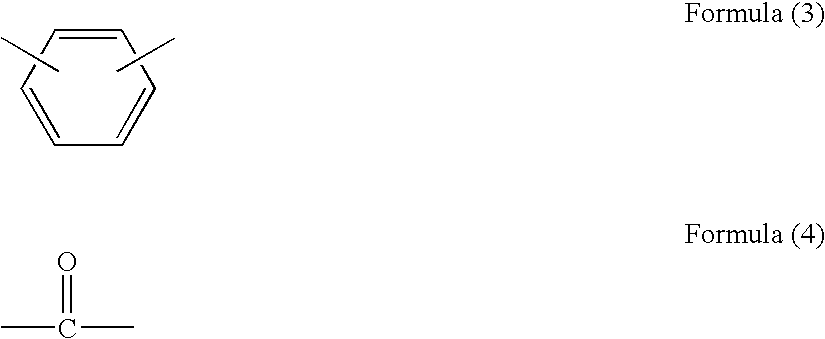
The group represented by each of A1, A2 and A3 may more preferably include a phenylene group, a carbonyl group, a vinylene group and a methylene group, which are respectively represented by formulas in the following Formula (2).
Figure US07276318-20071002-C00004
It may still more preferably be a phenylene group, which is represented by the following Formula (3):
Figure US07276318-20071002-C00005

a carbonyl group, which is represented by the following Formula (4):
Figure US07276318-20071002-C00006

a vinylene group, which is represented by the following Formula (5):
Figure US07276318-20071002-C00007
R1 and R2 may be the same or different and each independently represent an alkyl group such as a methyl group or an ethyl group, which may have a substituent, an aryl group such as a phenyl group or a naphthyl group, which may have a substituent, or a halogen atom such as a fluorine atom or a chlorine atom. The substituent may include alkyl groups such as a methyl group and an ethyl group, aryl groups such as a phenyl group and a naphthyl group, and halogen atoms such as a fluorine atom and a chlorine atom. m1 and m2 each represent an integer of 0 to 4.
R3, R4, R5 and R6 may be the same or different, and each independently represent a hydrogen atom, an alkyl group such as a methyl group or an ethyl group, which may have a substituent, an aryl group such as a phenyl group or a naphthyl group, which may have a substituent, a heterocyclic ring group such as furan, thiophene, pyridine, indole, benzothiazole, carbazole, acridone, benzoxazole, oxadiazole or thiazole; or an aralkyl group such as a benzyl group or a phenethyl group, which may have a substituent. The substituent may include alkyl groups such as methyl and ethyl; alkoxyl groups such as methoxyl and ethoxyl; halogen atoms such as a fluorine atom and a chlorine atom; dialkylamino groups such as dimethylamino and diethylamino; and a hydroxyl group, a nitro group, a cyano group, halomethyl groups, halomethoxyl groups, an acetyl group and a phenylcarbamoyl group. Incidentally, the phenyl group of this phenylcarbamoyl group may further have a substituent such as the one described above.
R3 and R4, and R5 and R6, may also each form a cyclic amino group via the nitrogen atom in the formula. The cyclic amino group containing a nitrogen atom in the ring may include pyrrole, pyrroline, pyrrolidine, pyrrolidone, indole, indoline, carbazole, imidazole, pyrazole, pyrazoline, oxazine and phenoxazine.
Z1 and Z2 each independently represent an oxygen atom or a sulfur atom.
In particular, a case in which R3 and R5 are each a hydrogen atom and Z1 and Z2 are each an oxygen atom is preferred in view of sensitivity. Further preferred in view of sensitivity is a case in which R4 and R6 are each independently an aryl group which may have a substituent, and further a case in which R4 and R6 are each independently a phenyl group which may have a substituent. Particularly preferred in view of sensitivity is a case in which R4 and R6 are each independently a phenyl group which has been substituted with at least one group selected from the group consisting of a chlorine atom, a fluorine atom, a bromine atom, an iodine atom, a nitro group, a trifluoromethyl group, a trifluoromethoxyl group, an acetyl group and a cyano group.
To describe more specifically the azo compound (bisazo pigment) represented by the above Formula (1), compounds having structures given in the following (i) to (xvi) may preferably be used in the present invention.
(i) A compound in which n1, n2 and n3 are 0.
(ii) A compound in which n1, n2 and n3 are 0, and also R3 and R5 are each a hydrogen atom, R4 and R6 are each independently a phenyl group substituted with at least one selected from the group consisting of a chlorine atom, a fluorine atom, a bromine atom, an iodine atom, a nitro group, a trifluoromethyl group, a trifluoromethoxyl group, an acetyl group and a cyano group, and Z1 and Z2 are each an oxygen atom.
(iii) A compound in which n1 is 1 and n2 and n3 are 0, and A1 is a group selected from the group consisting of groups represented by formulas in the above Formula (2).
(iv) A compound in which n1 is 1, n2 and n3 are each 0, A1 is a group selected from the group consisting of groups represented by the above Formula (2), R3 and R5 are each a hydrogen atom, R4 and R6 are each independently a phenyl group substituted with at least one selected from the group consisting of a chlorine atom, a fluorine atom, a bromine atom, an iodine atom, a nitro group, a trifluoromethyl group, a trifluoromethoxyl group, an acetyl group and a cyano group, and Z1 and Z2 are each an oxygen atom.
(v) A compound in which n1 is 1, n2 and n3 are each 0, and A1 is any one of groups represented by the above Formulas (3) to (5).
(vi) A compound in which n1 is 1 and n2 and n3 are 0, A1 is a group selected from the group consisting of groups represented by the above Formulas (3) to (5), R3 and R5 are each a hydrogen atom, R4 and R6 are each independently a phenyl group substituted with at least one selected from the group consisting of a chlorine atom, a fluorine atom, a bromine atom, an iodine atom, a nitro group, a trifluoromethyl group, a trifluoromethoxyl group, an acetyl group and a cyano group, and Z1 and Z2 are each an oxygen atom.
(vii) A compound in which n1 and n2 are 1 and n3 is 0, and A1 and A2 are each independently any one of groups represented by formulas in the above Formula (2).
(viii) A compound in which n1 and n2 are 1 and n3 is 0, A1 and A2 are each independently a group selected from the group consisting of groups represented by formulas in the above Formula (2), R3 and R5 are each a hydrogen atom, R4 and R6 are each independently a phenyl group substituted with at least one selected from the group consisting of a chlorine atom, a fluorine atom, a bromine atom, an iodine atom, a nitro group, a trifluoromethyl group, a trifluoromethoxyl group, an acetyl group and a cyano group, and Z1 and Z2 are each an oxygen atom.
(ix) A compound in which n1 and n2 are each 1, n3 is 0, A1 is a group represented by the above Formula (3), and A2 is a group represented by the above Formula (4).
(x) A compound in which n1 and n2 are each 1, n3 is 0, A1 is a group represented by the above Formula (3), A2 is a group represented by the above Formula (4), R3 and R5 are each a hydrogen atom, R4 and R6 are each independently a phenyl group susbstituted with at least one selected from the group consisting of a chlorine atom, a fluorine atom, a bromine atom, an iodine atom, a nitro group, a trifluoromethyl group, a trifluoromethoxyl group, an acetyl group and a cyano group, and Z1 and Z2 are each an oxygen atom.
(xi) A compound in which n1 and n2 are each 1, n3 is 0, A1 is a group represented by the above Formula (6), and A2 is a group represented by the above Formula (4).
(xii) A compound in which n1 and n2 are each 1, n3 is 0, A1 is a group represented by the above Formula (6), A2 is a group represented by the above Formula (4), R3 and R5 are each a hydrogen atom, R4 and R6 are each independently a phenyl group substituted with at least one selected from the group consisting of a chlorine atom, a fluorine atom, a bromine atom, an iodine atom, a nitro group, a trifluoromethyl group, a trifluoromethoxyl group, an acetyl group and a cyano group, and Z1 and Z2 are each an oxygen atom.
(xiii) A compound in which n1, n2 and n3 are each 1, A1, A2 and A3 are each independently a group selected from the group consisting groups represented by formulas in the above Formula (2).
(xiv) A compound in which n1, n2 and n3 are each 1, A1, A2 and A3 are each independently a group selected from the group consisting of groups represented by formulas in the above Formula (2), R3 and R5 are each a hydrogen atom, R4 and R6 are each independently a phenyl group substituted with at least one selected from the group consisting of a chlorine atom, a fluorine atom, a bromine atom, an iodine atom, a nitro group, a trifluoromethyl group, a trifluoromethoxyl group, an acetyl group and a cyano group, and Z1 and Z2 are each an oxygen atom.
(xv) A compound in which n1, n2 a6nd n3 are each 1, A1 and A2 are each a group represented by the above Formula (3), and A3 is a group represented by the above Formula (4).
(xvi) A compound in which n1, n2 and n3 are each 1, A1 and A2 are each a group represented by the above Formula (3), A3 is a group represented by the above Formula (4), R3 and R5 are each a hydrogen atom, R4 and R6 are each independently a phenyl group substituted with at least one selected from the group consisting of a chlorine atom, a fluorine atom, a bromine atom, an iodine atom, a nitro group, a trifluoromethyl group, a trifluoromethoxyl group, an acetyl group and a cyano group, and Z1 and Z2 are each an oxygen atom.
All the bisazo pigments may also have a crystal form which may be crystalline or may be amorphous.
Preferable exemplary compounds of the bisazo pigment which are usable in the present invention are enumerated below. Examples are by no means limited to these. As to structural formulas concerning the bisazo pigments, those represented by Formula (1) are grouped into Basic Pattern I, Basic Pattern II and Basic Pattern III in accordance with the position of substitution on the azo group, and only moieties corresponding to A1 to A3, R1 to R6, Z1 and Z2, and n1 to n3 are listed in Tables 1 to 14 (Exemplary Compound 1-1 to Exemplary Compound 14-5) in respect to the respective basic patterns.
Figure US07276318-20071002-C00008
TABLE 1
Case of n1 = n2 = n3 = 0 in Basic Pattern I
Exemplary
Compound R1 R2 Z1 Z2 R3 R4 R5 R6
1-1 O O H
Figure US07276318-20071002-C00009
H
Figure US07276318-20071002-C00010
1-2 O O H —CH3 H —CH3
1-3 O O H
Figure US07276318-20071002-C00011
H
Figure US07276318-20071002-C00012
1-4 O O H
Figure US07276318-20071002-C00013
H
Figure US07276318-20071002-C00014
1-5 O O H
Figure US07276318-20071002-C00015
H
Figure US07276318-20071002-C00016
1-6 O O H
Figure US07276318-20071002-C00017
H
Figure US07276318-20071002-C00018
1-7 O O H
Figure US07276318-20071002-C00019
H
Figure US07276318-20071002-C00020
1-8 O O H
Figure US07276318-20071002-C00021
H
Figure US07276318-20071002-C00022
1-9 O O H
Figure US07276318-20071002-C00023
H
Figure US07276318-20071002-C00024
1-10 O O —CH3
Figure US07276318-20071002-C00025
—CH3
Figure US07276318-20071002-C00026
1-11 O O H
Figure US07276318-20071002-C00027
H
Figure US07276318-20071002-C00028
1-12 O O H
Figure US07276318-20071002-C00029
H
Figure US07276318-20071002-C00030
1-13 O O H
Figure US07276318-20071002-C00031
H
Figure US07276318-20071002-C00032
1-14 O O H
Figure US07276318-20071002-C00033
H
Figure US07276318-20071002-C00034
1-15 O O H
Figure US07276318-20071002-C00035
H
Figure US07276318-20071002-C00036
TABLE 2
Case of n1 = n2 = n3 = 0 in Basic Pattern I
Exemplary
Compound R1 R2 Z1 Z2 R3 R4 R5 R6
2-1 O O
Figure US07276318-20071002-C00037
Figure US07276318-20071002-C00038
Figure US07276318-20071002-C00039
Figure US07276318-20071002-C00040
2-2 O O H
Figure US07276318-20071002-C00041
H
Figure US07276318-20071002-C00042
2-3 O O H
Figure US07276318-20071002-C00043
H
Figure US07276318-20071002-C00044
2-4 O O H
Figure US07276318-20071002-C00045
H
Figure US07276318-20071002-C00046
2-5 O O H
Figure US07276318-20071002-C00047
H
Figure US07276318-20071002-C00048
2-6 O O H
Figure US07276318-20071002-C00049
H
Figure US07276318-20071002-C00050
2-7 O O H
Figure US07276318-20071002-C00051
H
Figure US07276318-20071002-C00052
2-8 O O H
Figure US07276318-20071002-C00053
H
Figure US07276318-20071002-C00054
2-9 O O H
Figure US07276318-20071002-C00055
H
Figure US07276318-20071002-C00056
2-10 O O H
Figure US07276318-20071002-C00057
H
Figure US07276318-20071002-C00058
2-11 O O H
Figure US07276318-20071002-C00059
H
Figure US07276318-20071002-C00060
2-12 O O H
Figure US07276318-20071002-C00061
H
Figure US07276318-20071002-C00062
2-13 O O H
Figure US07276318-20071002-C00063
H
Figure US07276318-20071002-C00064
2-14 O O H
Figure US07276318-20071002-C00065
H
Figure US07276318-20071002-C00066
2-15 O O H
Figure US07276318-20071002-C00067
H
Figure US07276318-20071002-C00068
TABLE 3
Case of n1 = n2 = n3 = 0 in Basic Pattern I
Exemplary
Compound R1 R2 Z1 Z2 R3 R4 R5 R6
3-1 O O H
Figure US07276318-20071002-C00069
H
Figure US07276318-20071002-C00070
3-2 O O
Figure US07276318-20071002-C00071
Figure US07276318-20071002-C00072
3-3 O O H
Figure US07276318-20071002-C00073
H
Figure US07276318-20071002-C00074
3-4 O O H
Figure US07276318-20071002-C00075
H
Figure US07276318-20071002-C00076
3-5 Cl Cl O O H
Figure US07276318-20071002-C00077
H
Figure US07276318-20071002-C00078
3-6 Cl Cl O O H
Figure US07276318-20071002-C00079
H
Figure US07276318-20071002-C00080
3-7 CH3 CH3 O O H
Figure US07276318-20071002-C00081
H
Figure US07276318-20071002-C00082
3-8 CH3 CH3 O O H
Figure US07276318-20071002-C00083
H
Figure US07276318-20071002-C00084
3-9 S S H
Figure US07276318-20071002-C00085
H
Figure US07276318-20071002-C00086
3-10 S S H
Figure US07276318-20071002-C00087
H
Figure US07276318-20071002-C00088
3-11 O O H
Figure US07276318-20071002-C00089
H
Figure US07276318-20071002-C00090
3-12 O O H
Figure US07276318-20071002-C00091
H
Figure US07276318-20071002-C00092
3-13 O O H
Figure US07276318-20071002-C00093
H
Figure US07276318-20071002-C00094
3-14 O O H
Figure US07276318-20071002-C00095
H
Figure US07276318-20071002-C00096
TABLE 4
Case of n1 = n2 = n3 = 0 in Basic Pattern II
Exemplary
Compound R1 R2 Z1 Z2 R3 R4 R5 R6
4-1 O O H
Figure US07276318-20071002-C00097
H
Figure US07276318-20071002-C00098
4-2 O O H
Figure US07276318-20071002-C00099
H
Figure US07276318-20071002-C00100
4-3 O O H
Figure US07276318-20071002-C00101
H
Figure US07276318-20071002-C00102
4-4 O O H
Figure US07276318-20071002-C00103
H
Figure US07276318-20071002-C00104
4-5 O O H
Figure US07276318-20071002-C00105
H
Figure US07276318-20071002-C00106
4-6 O O H
Figure US07276318-20071002-C00107
H
Figure US07276318-20071002-C00108
4-7 Cl Cl O O H
Figure US07276318-20071002-C00109
H
Figure US07276318-20071002-C00110
4-8 Cl Cl O O H
Figure US07276318-20071002-C00111
H
Figure US07276318-20071002-C00112
4-9 F F O O H
Figure US07276318-20071002-C00113
H
Figure US07276318-20071002-C00114
4-10 CH3 CH3 O O H
Figure US07276318-20071002-C00115
H
Figure US07276318-20071002-C00116
4-11 O O H
Figure US07276318-20071002-C00117
H
Figure US07276318-20071002-C00118
TABLE 5
Case of n1 = n2 = n3 = 0 in Basic Pattern III
Exemplary
Compound R1 R2 Z1 Z2 R3 R4 R5 R6
5-1 O O H
Figure US07276318-20071002-C00119
H
Figure US07276318-20071002-C00120
5-2 O O H
Figure US07276318-20071002-C00121
H
Figure US07276318-20071002-C00122
5-3 O O H
Figure US07276318-20071002-C00123
H
Figure US07276318-20071002-C00124
5-4 O O H
Figure US07276318-20071002-C00125
H
Figure US07276318-20071002-C00126
5-5 O O H
Figure US07276318-20071002-C00127
H
Figure US07276318-20071002-C00128
5-6 O O H
Figure US07276318-20071002-C00129
H
Figure US07276318-20071002-C00130
5-7 O O
Figure US07276318-20071002-C00131
Figure US07276318-20071002-C00132
5-8 O O H —C2H5 H —C2H5
5-9 O O H
Figure US07276318-20071002-C00133
H
Figure US07276318-20071002-C00134
5-10 O O H
Figure US07276318-20071002-C00135
H
Figure US07276318-20071002-C00136
TABLE 6
Case of n1 = 1, n2 = n3 = 0 in Basic Pattern I
Exemplary
Compound R1 R2 Z1 Z2 A1 R3 R4 R5 R6
6-1 O O
Figure US07276318-20071002-C00137
H
Figure US07276318-20071002-C00138
H
Figure US07276318-20071002-C00139
6-2 O O
Figure US07276318-20071002-C00140
H
Figure US07276318-20071002-C00141
H
Figure US07276318-20071002-C00142
6-3 O O
Figure US07276318-20071002-C00143
Figure US07276318-20071002-C00144
Figure US07276318-20071002-C00145
Figure US07276318-20071002-C00146
Figure US07276318-20071002-C00147
6-4 O O
Figure US07276318-20071002-C00148
H
Figure US07276318-20071002-C00149
H
Figure US07276318-20071002-C00150
6-5 O O
Figure US07276318-20071002-C00151
H
Figure US07276318-20071002-C00152
H
Figure US07276318-20071002-C00153
6-6 O O
Figure US07276318-20071002-C00154
H
Figure US07276318-20071002-C00155
H
Figure US07276318-20071002-C00156
6-7 S S
Figure US07276318-20071002-C00157
H
Figure US07276318-20071002-C00158
H
Figure US07276318-20071002-C00159
6-8 O O
Figure US07276318-20071002-C00160
H
Figure US07276318-20071002-C00161
H
Figure US07276318-20071002-C00162
6-9 O O
Figure US07276318-20071002-C00163
Figure US07276318-20071002-C00164
Figure US07276318-20071002-C00165
6-10 O O
Figure US07276318-20071002-C00166
H
Figure US07276318-20071002-C00167
H
Figure US07276318-20071002-C00168
6-11 O O
Figure US07276318-20071002-C00169
H
Figure US07276318-20071002-C00170
H
Figure US07276318-20071002-C00171
6-12 O O
Figure US07276318-20071002-C00172
H
Figure US07276318-20071002-C00173
H
Figure US07276318-20071002-C00174
6-13 O O
Figure US07276318-20071002-C00175
H
Figure US07276318-20071002-C00176
H
Figure US07276318-20071002-C00177
6-14 O O
Figure US07276318-20071002-C00178
H
Figure US07276318-20071002-C00179
H
Figure US07276318-20071002-C00180
6-15 O O
Figure US07276318-20071002-C00181
H
Figure US07276318-20071002-C00182
H
Figure US07276318-20071002-C00183
TABLE 7
Case of n1 = 1, n2 = n3 = 0 in Basic Pattern I
Exemplary
Compound R1 R2 Z1 Z2 A1 R3 R4 R5 R6
7-1 O O
Figure US07276318-20071002-C00184
H
Figure US07276318-20071002-C00185
H
Figure US07276318-20071002-C00186
7-2 O O
Figure US07276318-20071002-C00187
H
Figure US07276318-20071002-C00188
H
Figure US07276318-20071002-C00189
7-3 O O
Figure US07276318-20071002-C00190
H
Figure US07276318-20071002-C00191
H
Figure US07276318-20071002-C00192
7-4 O O
Figure US07276318-20071002-C00193
H
Figure US07276318-20071002-C00194
H
Figure US07276318-20071002-C00195
7-5 O O
Figure US07276318-20071002-C00196
H
Figure US07276318-20071002-C00197
H
Figure US07276318-20071002-C00198
7-6 O O
Figure US07276318-20071002-C00199
H
Figure US07276318-20071002-C00200
H
Figure US07276318-20071002-C00201
7-7 O O
Figure US07276318-20071002-C00202
H
Figure US07276318-20071002-C00203
H
Figure US07276318-20071002-C00204
7-8 O O
Figure US07276318-20071002-C00205
H
Figure US07276318-20071002-C00206
H
Figure US07276318-20071002-C00207
7-9 O O —CH2— H
Figure US07276318-20071002-C00208
H
Figure US07276318-20071002-C00209
7-10 O O —CH2— —CH3
Figure US07276318-20071002-C00210
—CH3
Figure US07276318-20071002-C00211
7-11 O O
Figure US07276318-20071002-C00212
H
Figure US07276318-20071002-C00213
H
Figure US07276318-20071002-C00214
7-12 O O
Figure US07276318-20071002-C00215
H
Figure US07276318-20071002-C00216
H
Figure US07276318-20071002-C00217
7-13 O O
Figure US07276318-20071002-C00218
H
Figure US07276318-20071002-C00219
H
Figure US07276318-20071002-C00220
7-14 O O
Figure US07276318-20071002-C00221
H
Figure US07276318-20071002-C00222
H
Figure US07276318-20071002-C00223
7-15 O O
Figure US07276318-20071002-C00224
H
Figure US07276318-20071002-C00225
H
Figure US07276318-20071002-C00226
TABLE 8
Case of n1 = 1, n2 = n3 = 0 in Basic Pattern II
Exemplary
Compound R1 R2 Z1 Z2 A1 R3 R4 R5 R6
8-1 O O
Figure US07276318-20071002-C00227
H
Figure US07276318-20071002-C00228
H
Figure US07276318-20071002-C00229
8-2 O O
Figure US07276318-20071002-C00230
H
Figure US07276318-20071002-C00231
H
Figure US07276318-20071002-C00232
8-3 O O
Figure US07276318-20071002-C00233
H
Figure US07276318-20071002-C00234
H
Figure US07276318-20071002-C00235
8-4 O O
Figure US07276318-20071002-C00236
H
Figure US07276318-20071002-C00237
H
Figure US07276318-20071002-C00238
8-5 O O
Figure US07276318-20071002-C00239
H
Figure US07276318-20071002-C00240
H
Figure US07276318-20071002-C00241
8-6 Cl Cl O O
Figure US07276318-20071002-C00242
H
Figure US07276318-20071002-C00243
H
Figure US07276318-20071002-C00244
8-7 O O
Figure US07276318-20071002-C00245
H
Figure US07276318-20071002-C00246
H
Figure US07276318-20071002-C00247
8-8 S S
Figure US07276318-20071002-C00248
H
Figure US07276318-20071002-C00249
H
Figure US07276318-20071002-C00250
8-9 Cl Cl O O
Figure US07276318-20071002-C00251
H
Figure US07276318-20071002-C00252
H
Figure US07276318-20071002-C00253
8-10 O O —CH2— H
Figure US07276318-20071002-C00254
H
Figure US07276318-20071002-C00255
TABLE 9
Case of n1 = 1, n2 = n3 = 0 in Basic Pattern III
Exemplary
Compound R1 R2 Z1 Z2 A1 R3 R4 R5 R6
9-1 O O
Figure US07276318-20071002-C00256
H
Figure US07276318-20071002-C00257
H
Figure US07276318-20071002-C00258
9-2 O O
Figure US07276318-20071002-C00259
H
Figure US07276318-20071002-C00260
H
Figure US07276318-20071002-C00261
9-3 O O
Figure US07276318-20071002-C00262
H
Figure US07276318-20071002-C00263
H
Figure US07276318-20071002-C00264
9-4 O O
Figure US07276318-20071002-C00265
H
Figure US07276318-20071002-C00266
H
Figure US07276318-20071002-C00267
9-5 O O
Figure US07276318-20071002-C00268
H
Figure US07276318-20071002-C00269
H
Figure US07276318-20071002-C00270
9-6 O O
Figure US07276318-20071002-C00271
H
Figure US07276318-20071002-C00272
H
Figure US07276318-20071002-C00273
9-7 CH3 CH3 O O
Figure US07276318-20071002-C00274
H
Figure US07276318-20071002-C00275
H
Figure US07276318-20071002-C00276
9-8 O O
Figure US07276318-20071002-C00277
H
Figure US07276318-20071002-C00278
H
Figure US07276318-20071002-C00279
9-9 O O
Figure US07276318-20071002-C00280
H
Figure US07276318-20071002-C00281
H
Figure US07276318-20071002-C00282
9-10 O O —CH2— H
Figure US07276318-20071002-C00283
H
Figure US07276318-20071002-C00284
TABLE 10
Case of n1 = n2 = 1, n3 = 0 in Basic Pattern I
Exemplary
Compound R1 R2 Z1 Z2 A1 A2 R3 R4 R5 R6
10-1 O O
Figure US07276318-20071002-C00285
Figure US07276318-20071002-C00286
H
Figure US07276318-20071002-C00287
H
Figure US07276318-20071002-C00288
10-2 O O
Figure US07276318-20071002-C00289
Figure US07276318-20071002-C00290
H
Figure US07276318-20071002-C00291
H
Figure US07276318-20071002-C00292
10-3 O O
Figure US07276318-20071002-C00293
Figure US07276318-20071002-C00294
H
Figure US07276318-20071002-C00295
H
Figure US07276318-20071002-C00296
10-4 O O —CH2—
Figure US07276318-20071002-C00297
H
Figure US07276318-20071002-C00298
H
Figure US07276318-20071002-C00299
10-5 O O
Figure US07276318-20071002-C00300
Figure US07276318-20071002-C00301
H
Figure US07276318-20071002-C00302
H
Figure US07276318-20071002-C00303
10-6 O O
Figure US07276318-20071002-C00304
Figure US07276318-20071002-C00305
H
Figure US07276318-20071002-C00306
H
Figure US07276318-20071002-C00307
10-7 O O
Figure US07276318-20071002-C00308
Figure US07276318-20071002-C00309
H
Figure US07276318-20071002-C00310
H
Figure US07276318-20071002-C00311
10-8 O O
Figure US07276318-20071002-C00312
Figure US07276318-20071002-C00313
H
Figure US07276318-20071002-C00314
H
Figure US07276318-20071002-C00315
10-9 O O
Figure US07276318-20071002-C00316
Figure US07276318-20071002-C00317
H
Figure US07276318-20071002-C00318
H
Figure US07276318-20071002-C00319
10-10 O O
Figure US07276318-20071002-C00320
—CH2— H
Figure US07276318-20071002-C00321
H
Figure US07276318-20071002-C00322
10-11 O O
Figure US07276318-20071002-C00323
Figure US07276318-20071002-C00324
H
Figure US07276318-20071002-C00325
H
Figure US07276318-20071002-C00326
10-12 O O
Figure US07276318-20071002-C00327
Figure US07276318-20071002-C00328
H
Figure US07276318-20071002-C00329
H
Figure US07276318-20071002-C00330
10-13 O O
Figure US07276318-20071002-C00331
Figure US07276318-20071002-C00332
H
Figure US07276318-20071002-C00333
H
Figure US07276318-20071002-C00334
10-14 O O
Figure US07276318-20071002-C00335
Figure US07276318-20071002-C00336
H
Figure US07276318-20071002-C00337
H
Figure US07276318-20071002-C00338
10-15 O O
Figure US07276318-20071002-C00339
Figure US07276318-20071002-C00340
H
Figure US07276318-20071002-C00341
H
Figure US07276318-20071002-C00342
TABLE 11
Case of n1 = n2 = 1, n3 = 0 in Basic Pattern II
Exemplary
Compound R1 R2 Z1 Z2 A1 A2 R3 R4 R5 R6
11-1 O O
Figure US07276318-20071002-C00343
Figure US07276318-20071002-C00344
H
Figure US07276318-20071002-C00345
H
Figure US07276318-20071002-C00346
11-2 O O —CH2— —CH2— H
Figure US07276318-20071002-C00347
H
Figure US07276318-20071002-C00348
11-3 O O —CH2—
Figure US07276318-20071002-C00349
H
Figure US07276318-20071002-C00350
H
Figure US07276318-20071002-C00351
11-4 O O
Figure US07276318-20071002-C00352
Figure US07276318-20071002-C00353
H
Figure US07276318-20071002-C00354
H
Figure US07276318-20071002-C00355
11-5 O O
Figure US07276318-20071002-C00356
Figure US07276318-20071002-C00357
H
Figure US07276318-20071002-C00358
H
Figure US07276318-20071002-C00359
11-6 O O
Figure US07276318-20071002-C00360
Figure US07276318-20071002-C00361
H
Figure US07276318-20071002-C00362
H
Figure US07276318-20071002-C00363
11-7 O O
Figure US07276318-20071002-C00364
Figure US07276318-20071002-C00365
H
Figure US07276318-20071002-C00366
H
Figure US07276318-20071002-C00367
11-8 O O
Figure US07276318-20071002-C00368
Figure US07276318-20071002-C00369
H
Figure US07276318-20071002-C00370
H
Figure US07276318-20071002-C00371
11-9 O O
Figure US07276318-20071002-C00372
Figure US07276318-20071002-C00373
H
Figure US07276318-20071002-C00374
H
Figure US07276318-20071002-C00375
11-10 O O
Figure US07276318-20071002-C00376
Figure US07276318-20071002-C00377
H
Figure US07276318-20071002-C00378
H
Figure US07276318-20071002-C00379
TABLE 12
Case of n1 = n2 = 1, n3 = 0 in Basic Pattern III
Exemplary
Compound R1 R2 Z1 Z2 A1 A2 R3 R4 R5 R6
12-1 O O
Figure US07276318-20071002-C00380
Figure US07276318-20071002-C00381
H
Figure US07276318-20071002-C00382
H
Figure US07276318-20071002-C00383
12-2 O O
Figure US07276318-20071002-C00384
Figure US07276318-20071002-C00385
H
Figure US07276318-20071002-C00386
H
Figure US07276318-20071002-C00387
12-3 O O
Figure US07276318-20071002-C00388
Figure US07276318-20071002-C00389
H
Figure US07276318-20071002-C00390
H
Figure US07276318-20071002-C00391
12-4 O O
Figure US07276318-20071002-C00392
Figure US07276318-20071002-C00393
H
Figure US07276318-20071002-C00394
H
Figure US07276318-20071002-C00395
12-5 O O
Figure US07276318-20071002-C00396
Figure US07276318-20071002-C00397
H
Figure US07276318-20071002-C00398
H
Figure US07276318-20071002-C00399
TABLE 13
Case of n1 = n2 = n3 = 1 in Basic Pattern I
Exemplary
Com-
pound R1 R2 Z1 Z2 A1 A2 A3 R3 R4 R5 R6
13-1 O O
Figure US07276318-20071002-C00400
Figure US07276318-20071002-C00401
Figure US07276318-20071002-C00402
H
Figure US07276318-20071002-C00403
H
Figure US07276318-20071002-C00404
13-2 O O
Figure US07276318-20071002-C00405
Figure US07276318-20071002-C00406
Figure US07276318-20071002-C00407
H
Figure US07276318-20071002-C00408
H
Figure US07276318-20071002-C00409
13-3 O O
Figure US07276318-20071002-C00410
Figure US07276318-20071002-C00411
Figure US07276318-20071002-C00412
H
Figure US07276318-20071002-C00413
H
Figure US07276318-20071002-C00414
13-4 O O
Figure US07276318-20071002-C00415
Figure US07276318-20071002-C00416
Figure US07276318-20071002-C00417
H
Figure US07276318-20071002-C00418
H
Figure US07276318-20071002-C00419
13-5 O O
Figure US07276318-20071002-C00420
Figure US07276318-20071002-C00421
Figure US07276318-20071002-C00422
H
Figure US07276318-20071002-C00423
H
Figure US07276318-20071002-C00424
TABLE 14
Case of n1 = n2 = n3 = 1 in Basic Pattern II
Exemplary
Com-
pound R1 R2 Z1 Z2 A1 A2 A3 R3 R4 R5 R6
14-1 O O
Figure US07276318-20071002-C00425
Figure US07276318-20071002-C00426
Figure US07276318-20071002-C00427
H
Figure US07276318-20071002-C00428
H
Figure US07276318-20071002-C00429
14-2 O O
Figure US07276318-20071002-C00430
Figure US07276318-20071002-C00431
Figure US07276318-20071002-C00432
H
Figure US07276318-20071002-C00433
H
Figure US07276318-20071002-C00434
14-3 O O
Figure US07276318-20071002-C00435
Figure US07276318-20071002-C00436
Figure US07276318-20071002-C00437
H
Figure US07276318-20071002-C00438
H
Figure US07276318-20071002-C00439
14-4 O O
Figure US07276318-20071002-C00440
Figure US07276318-20071002-C00441
Figure US07276318-20071002-C00442
H
Figure US07276318-20071002-C00443
H
Figure US07276318-20071002-C00444
14-5 O O
Figure US07276318-20071002-C00445
—CH2—
Figure US07276318-20071002-C00446
H
Figure US07276318-20071002-C00447
H
Figure US07276318-20071002-C00448
Of the bisazo pigments according to the present invention which are shown in the above Tables 1 to 14, bisazo pigments of the following Exemplary Compound Numbers have especially superior sensitivity to the blue (purple) semiconductor laser light used as writing light for forming electrostatic latent images on the photosensitive member, and hence are those particularly preferably usable in the present invention.
Exemplary Compound Nos.:
1-8, 1-11, 1-12, 1-13, 1-14, 1-15;
2-2, 2-4, 2-9, 2-10, 2-11, 2-12, 2-13, 2-14;
3-4;
6-1, 6-4, 6-11, 6-12, 6-13, 6-14;
7-3, 7-5, 7-11, 7-12, 7-13; and
10-11.
Further, of the bisazo compounds of the above Exemplary Compound Numbers, bisazo compounds having symmetrical structures shown as Exemplary Compounds Nos. 1-11 and 2-4 and bisazo compounds having asymmetrical structures shown as Exemplary Compounds Nos. 1-12, 1-13, 1-14, 1-15, 2-9, 2-10, 2-11, 2-12, 2-13, 2-14 and 3-4 are those which afford photosensitive members having superior sensitivity also when white light is used as writing light.
The above bisazo pigment may be used in combination of two or more types. Also optionally usable in the form of a mixture with the above is a charge-generating material including cationic dyes such as pyrylium dyes, thiapyrylium dyes, azulenium dyes, thiacyanine dyes and quinocyanine dyes, squalium salt dyes, azo pigments other than the above bisazo pigment, polycyclic quinone pigments such as anthanthrone pigments, dibenzopyrenequinone pigments and pyranthrone pigments, indigo pigments, quinacridone pigments, perylene pigments and phthalocyanine pigments.
The binder resin used to form the charge generation layer may be selected from comprehensive insulating resins or organic photoconductive polymers. Preferred are polyvinyl butyral, polyvinyl benzal, polyarylates, polycarbonates, polyesters, phenoxy resins, cellulose resins, acrylic resins, and polyurethanes, as well as copolymers of two or more of these. These resins may have a substituent. As the substituent, preferred are a halogen atom, an alkyl group, an alkoxyl group, a nitro group, a cyano group, a trifluoromethyl group and so forth. The binder resin may also preferably be used in an amount of 80% by weight or less, and more preferably 60% by weight or less, based on the total weight of the charge generation layer.
The charge generation layer may be formed by coating a charge generation layer coating dispersion obtained by dispersing the charge-generating material together with the binder resin and a solvent, followed by drying. As a method for dispersion, a method is available which makes use of a homogenizer, ultrasonic waves, a ball mill, a sand mill, an attritor, a roll mill or the like. The charge-generating material and the binder resin may preferably be in a proportion ranging from 1:0.1 to 1:4 (weight ratio).
As the solvent used for the charge generation layer coating dispersion, it may be selected taking account of the binder resin to be used and the solubility or dispersion stability of the charge-generating material. It may include, e.g., ethers such as tetrahydrofuran, 1,4-dioxane and 1,2-dimethoxyethane, ketones such as cyclohexanone, methyl ethyl ketone and pentanone, amines such as N,N-dimethylformamide, esters such as methyl acetate and ethyl acetate, aromatics such as toluene, xylene and chlorobenzene, alcohols such as methanol, ethanol and 2-propanol, and aliphatic halogenated hydrocarbons such as chloroform, methylene chloride, dichloroethylene, carbon tetrachloride, and trichloroethylene.
When the charge generation layer coating solution is coated, coating methods as exemplified by dip coating, spray coating, spinner coating, roller coating, Mayer bar coating and blade coating may be used.
The charge generation layer may also preferably be in a layer thickness of 5 μm or less, and particularly more preferably from 0.1 μm to 2 μm.
To the charge generation layer, a sensitizer, an antioxidant, an ultraviolet absorber, a plasticizer, a thickening agent and so forth which may be of various types may also optionally be added.
A charge transport layer is provided on the charge generation layer.
The charge transport layer has the function to receive charged carriers from the charge generation layer in the presence of an electric field and transport the same. The charge transport layer may be formed by coating a coating solution prepared by dissolving a charge-transporting material in a solvent together with a binder resin, followed by drying. It may preferably be in a layer thickness of from 5 μm to 40 μm, more preferably from 5 μm to 30 μm, and still more preferably from 5 μm to 20 μm.
The charge-transporting material includes an electron-transporting material and a hole-transporting material.
The electron-transporting material may include, e.g., electron-attracting substances such as 2,4,7-trinitrofluorenone, 2,4,5,7-tetranitrofluorenone, chloranil and tetracyanoquinodimethane, and those obtained by polymerizing these electron-attracting substances.
The hole-transporting material may include, e.g., polycyclic aromatic compounds such as pyrene and anthracene, heterocyclic compounds such as carbazole compounds, indole compounds, oxazole compounds, thiazole compounds, oxadiazole compounds, pyrazole compounds, pyrazoline compounds, thiadiazole compounds and triazole compounds, hydrazone compounds, styryl compounds, benzidine compounds, triarylmethane compounds, and triphenylamine compounds.
Any of these charge-transporting materials may be used alone or in combination of two or more types.
Where the charge-transporting material has no film-forming properties, a suitable binder resin may be used. The binder resin used for the charge transport layer may include, e.g., insulating resins such as acrylic resins, polyarylates, polycarbonates, polyesters, polystyrene, an acrylonitrile-styrene copolymer, polyacrylamide, polyamide and chlorinated rubber, and organic photoconductive polymers such as poly-N-vinyl carbazole and polyvinyl anthracene. One or two or more of any of these may be used alone or in the form of a mixture or copolymer.
A photoconductive resin may also be used which functions as both the charge-transporting material and the binder resin, such as a polymer (e.g., poly-N-vinyl carbazole, polyvinyl anthracene) having in the backbone chain or side chain a group derived from the above charge-transporting material.
However, in the case when the photosensitive layer has the layer configuration as shown in FIG. 1 in which the charge generation layer and the charge transport layer are superposed on the support in this order and such one is used in the electrophotographic photosensitive member, it is necessary to select a charge-transporting material and a binder resin which have high transmittance in respect to the lasing wavelength of the semiconductor laser to be used.
As the solvent used in the charge transport layer coating solution, usable are ketones such as acetone and methyl ethyl ketone, ethers such as tetrahydrofuran and dimethoxymethane, esters such as methyl acetate and ethyl acetate, aromatic hydrocarbons such as toluene and xylene, and hydrocarbons substituted with a halogen atom, such as chlorobenzene, chloroform and carbon tetrachloride.
When the charge transport layer coating solution is coated, coating methods as exemplified by dip coating, spray coating, spinner coating, roller coating, Mayer bar coating and blade coating may be used.
To the charge transport layer, an antioxidant, an ultraviolet absorber, a plasticizer, a filler and so forth may also optionally be added.
In the case when the photosensitive layer is of a single-layer type, such a single-layer type photosensitive layer may be formed by coating a single-layer type photosensitive layer coating dispersion obtained by dispersing the charge-generating material and the charge-transporting material together with the binder resin and the solvent, followed by drying.
A protective layer may also be provided on the photosensitive layer, for the purpose of protecting the photosensitive layer from mechanical external force, chemical external force and so forth and also for the purpose of improving transfer performance and cleaning performance.
The protective layer may be formed by coating a protective layer coating solution obtained by dissolving a resin such as polyvinyl butyral, polyester, polycarbonate, polyamide, polyimide, polyarylate, polyurethane, a styrene-butadiene copolymer, a styrene-acrylic acid copolymer or a styrene-acrylonitrile copolymer in a solvent, followed by drying.
In order to make the protective layer have charge transport performance together, the protective layer may also be formed by curing a monomer material having charge transport performance, or a polymer type charge-transporting material, by cross-linking reaction of various types. The reaction by which it is cured may include radical polymerization, ion polymerization, thermal polymerization, photopolymerization, radiation polymerization (electron ray polymerization), plasma-assisted CVD and photo-assisted CVD.
The protective layer may further be incorporated with conductive particles, an ultraviolet absorbent, a wear resistance improver and so forth. As the conductive particles, metal oxides as exemplified by tin oxide particles are preferred. As the wear resistance improver, fine fluorine resin powders, alumina, silica and the like are preferred.
The protective layer may preferably be in a layer thickness of from 0.5 μm to 20 μm, and particularly preferably from 1 μm to 10 μm.
The, surface layer of the organic photosensitive member is meant to be the charge transport layer in what is shown in FIG. 1, the charge generation layer in what is shown in FIG. 2, and the photosensitive layer in what is shown in FIG. 3.
Next, an example of the electrophotographic apparatus having the electrophotographic photosensitive member of the present invention is shown in FIG. 4 as a schematic sectional view. What is shown in FIG. 4 is a full-color electrophotographic apparatus, which has a digital full-color-image reader section at the top and a digital full-color-image printer section at a lower part.
In the reader section, an original 30 is placed on an original-setting glass 31, and an exposure lamp 32 is put into exposure scanning, whereby an optical image reflected from the original 30 is focused on a full-color sensor 34 through a lens 33 to obtain full-color color separation image signals. The full-color color separation image signals are processed by a video processing unit (not shown) through an amplifying circuit (not shown), and then forwarded to the printer section.
In the printer section, reference numeral 1 denotes an electrophotographic photosensitive member, which is supported rotatably in the direction of an arrow. Around the electrophotographic photosensitive member 1, provided are a pre-exposure lamp 11 (destaticizing means), a corona charging assembly 12 (charging means), a laser exposure optical system 3 (exposure means), a potential sensor 12, different color, four developing assemblies 4 y, 4 c, 4 m and 4Bk (developing means), a detecting means 13 for detecting the amount of light on the surface of the electrophotographic photosensitive member, a transfer means 5, and a cleaner 6 (cleaning means).
The laser exposure optical system 3 has the blue (purple) semiconductor laser. Its lasing wavelength may preferably be from 380 nm to 500 nm, and more preferably from 380 nm to 450 nm. As types of the laser, a ZnSe semiconductor laser and a GaN semiconductor laser are preferred. In particular, the GaN semiconductor laser is preferred. With regard to laser exposure output, it may preferably be 1 mW or more, more preferably 3 mW or more, and particularly preferably 5 mW or more.
In the laser exposure optical system 3, the image signals sent from the reader section are converted in a laser output section (not shown) into optical signals for image scanning exposure, and the laser beam thus converted is reflected on a polygonal mirror 3 a and projected on the surface of the electrophotographic photosensitive member 1 through a lens 3 b and a mirror 3 c. Writing pitch is set to about 400 dpi to about 2,400 dpi; and the beam spot diameter, to about 15 μm to about 40 μm.
At the time of image formation in the printer section, the electrophotographic photosensitive member 1 is rotated in the direction of the arrow. The electrophotographic photosensitive member 1 is, after destaticized by the exposure lamp 11, uniformly negatively electrostatically charged by means of the charging assembly 2, and then irradiated with an optical image E for each separated color to form electrostatic latent images on the surface of the electrophotographic photosensitive member 1.
Next, a stated developing assembly is operated to develop the electrostatic latent images formed on the surface of the electrophotographic photosensitive member 1, to form developed images on the surface of the electrophotographic photosensitive member 1 by the use of a one-component developer (a toner) or two-component developer (each making use of a negative toner) composed of a resin as a base material. The developing assemblies are so set as to alternatively come close to the electrophotographic photosensitive member 1 in accordance with the respective separated colors by the operation of eccentric cams 24 y, 24 c, 24 m and 24Bk.
Developed images held on the surface of the electrophotographic photosensitive member 1 are further transferred to a sheet of paper (transfer material) which has been fed from a transfer material cassette 7 in which sheets of paper which are transfer materials are kept held, through a transport system and a transfer means 5 and to the position facing the electrophotographic photosensitive member 1. The transfer means 5 has, in this example, a transfer drum 5 a, a transfer charging assembly 5 b, an attraction charging assembly 5 c for attracting a sheet of paper (transfer material) electrostatically, an attraction roller 5 g provided opposingly thereto, an inside charging assembly 5 d, and an outside charging assembly 5 e. The transfer drum 5 a, which is axially supported so that it can rotatingly be driven, has a transfer material holding sheet 5 f made of a dielectric material, which is stretched integrally in a cylindrical form at an open zone on the periphery thereof. As the transfer material holding sheet 5 f, a dielectric-material sheet such as polycarbonate film is used.
As the transfer drum 5 a is rotated, the developed images on the surface of the electrophotographic photosensitive member 1 are transferred by means of the transfer charging assembly 5 b to the sheet of paper (transfer material) held on the transfer material holding sheet 5 f of the transfer drum 5 a.
In this way, a desired number of color images are transferred to the sheet of paper (transfer material) attracted to and transported on the transfer material holding sheet 5 f, thus a full-color image is formed.
In the case when the full-color image is formed, the transfer of four-color developed images is thus completed, whereupon the sheet of paper (transfer material) is separated from the transfer drum 5 a by the action of a separation claw 8 a, a separation push-up roller 8 b and a separation charging assembly 5 h, and then put out to a tray 10 via a heat roller fixing assembly 9.
Meanwhile, the electrophotographic photosensitive member 1 after transfer is cleaned by removing with the cleaner 6 the toners remaining on the surface, and thereafter again put to the steps of image formation.
When the image is formed on the both sides of the sheet of paper (transfer material), immediately after the paper has been delivered out of the fixing assembly 9, a transport path switch guide 19 is driven to first guide the paper to a reverse path 21 a via a transport vertical path 20, and then reverse rollers 21 b are rotated in reverse so that the sheet of paper is withdrawn in the direction opposite to the direction in which it has been sent into the rollers, with its leading end first which had been the rear end when sent into the rollers, and is received in an intermediate tray 22. Thereafter, an image is formed again on the other side through the image formation steps described above.
In order to, e.g., prevent powder from scattering and adhering onto the transfer material holding sheet 5 f of the transfer drum 5 a and prevent oil from adhering onto the paper (transfer material), cleaning is also performed by the action of a fur brush 14 and a back-up brush 15 set opposingly to the fur brush 14 via the transfer material holding sheet 5 f, and an oil-removing roller 16 and a back-up brush 17 set opposingly to the oil-removing roller 16 via the transfer material holding sheet 5 f. Such cleaning may be performed before the image formation or after the image formation, or may be performed at any time when a jam (paper jam) occurs.
In this example, an eccentric cam 25 is also operated at desired timing to actuate a cam follower 5 i associated with the transfer drum 5 a, whereby the gap between the transfer material holding sheet 5 f and the electrophotographic photosensitive member 1 can be set as desired. For example, during a stand-by or at the time of power-off, a space is kept between the transfer drum 5 a and the electrophotographic photosensitive member 1.
Next, an example of a process cartridge having the electrophotographic photosensitive member of the present invention is shown in FIG. 5 as a schematic sectional view.
In the apparatus shown in FIG. 5, at least an electrophotographic photosensitive member 1, a corona charging assembly 2 and a developing means 4 are received in a container 35 to make up a process cartridge. The process cartridge is so constructed as to be detachably mountable to the main body of the apparatus by the use of a guide means 34 such as rails. The cleaning means 6 need not necessarily be provided in the container 35.
As also shown in FIGS. 6 and 7, a contact charging member 2 a may be employed as the charging means, and the contact charging member 2 a, to which a voltage is kept applied, may be brought into contact with the electrophotographic photosensitive member 1 to charge the electrophotographic photosensitive member electrostatically (hereinafter, this charging system is called contact charging). In the apparatus shown in FIGS. 6 and 7, the toner image held on the electrophotographic photosensitive member is transferred also by a contact transfer means 5 i to a transfer material 7 a. More specifically, the contact transfer means 5 i, to which a voltage is kept applied, is brought into contact with the transfer material 7 a to transfer to the transfer material 7 a the toner image held on the electrophotographic photosensitive member.
In addition, in the apparatus shown in FIG. 7, at least the electrophotographic photosensitive member 1 and the contact charging member 2 a are received in a first container 36 to make up a first process cartridge, and at least the developing means 4 is received in a second container 37 to make up a second process cartridge. These first process cartridge and second process cartridge are so constructed as to be detachably mountable to the main body of the apparatus. The cleaning means 6 need not necessarily be provided.
A developer (toner) used in the electrophotographic apparatus having the electrophotographic photosensitive member of the present invention is described next.
The toner used in the present invention may preferably have a specific particle size distribution. If toner particles of 5 μm or less in particle diameter are less than 17% by number, the toner tends to be consumed in a large quantity. In addition, if the toner has a volume-average particle diameter Dv (μm) of 8 μm or more and a weight-average particle diameter D4 (μm) of 9 μm or more, the resolution of dots of 100 μm or less in diameter tends to lower, and this tendency is more remarkable in regard to the resolution of dots of 15 to 40 μm that is achievable in the present invention. In such a case, even if it is attempted to perform development according to unnatural designing under different development conditions, it is difficult to achieve stable developing performance, such that thick-line images or toner scatter tends to occur or the toner may be consumed in a large quantity.
If on the other hand toner particles of 5 μm or less in particle diameter are more than 90% by number, it may be difficult to perform development stably, to cause a difficulty such that the image density decreases. In order to more improve resolution, the toner may preferably be a toner having fine particle diameter of 3.0 μm≦Dv≦6.0 μm and 3.5 μm≦D4≦6.5 μm, which may further preferably be 3.2 μm≦Dv≦5.8 μm and 3.6 μm≦D4≦6.3 μm.
As a binder resin used in the toner, it may include styrene homopolymers or copolymers such as polystyrene, a styrene-acrylate copolymer, a styrene-methacrylate copolymer and a styrene-butadiene copolymer, polyester resins, epoxy resins, and petroleum resins.
In view of an improvement in releasability from a fixing member and an improvement in fixing performance at the time of fixing, it is preferable to incorporate in the toner such a wax as shown below. The wax may include paraffin wax and derivatives thereof, microcrystalline wax and derivatives thereof, Fischer-Tropsch wax and derivatives thereof, polyolefin wax and derivatives thereof, and carnauba wax and derivatives thereof. The derivatives include oxides, block copolymers with vinyl monomers, and graft modified products. Besides, also usable are long-chain alcohols, long-chain fatty acids, acid amide compounds, ester compounds, ketone compounds, hardened caster oil and derivatives thereof, vegetable waxes, animal waxes, mineral waxes and petrolatums.
As a colorant used in the toner, an inorganic pigment, an organic dye and an organic pigment which are conventionally known may be used. It may include, e.g., carbon black, Aniline Black, acetylene black, Naphthol Yellow, Hanza Yellow, Rhodamine Lake, Alizarine Lake, red iron oxide, Phthalocyanine Blue and Indanethrene Blue. Any of these may usually be used in an amount of from 0.5 to 20 parts by weight based on 100 parts by weight of the binder resin.
A magnetic material may also be used as a component constituting the toner. The magnetic material may include magnetic metal oxides containing an element such as iron, cobalt, nickel, copper, magnesium, manganese, aluminum or silicon. Of these, those composed chiefly of a magnetic iron oxide such as triiron tetraoxide and γ-iron oxide are preferred.
For the purpose of charge control of the toner, also usable are a Nigrosine dye, a quaternary ammonium salt, a salicylic acid metal complex, a salicylic acid metal salt, a salicylic acid derivative metal complex, salicylic acid, acetylacetone and the like.
The toner used in the electrophotographic apparatus having the electrophotographic photosensitive member of the present invention may. preferably have an inorganic fine powder on toner particle surfaces. This is effective for improving development efficiency, reproducibility of electrostatic latent images, and transfer efficiency, and making fog less occur.
The inorganic fine powder may include, e.g., fine powders formed of colloidal silica, titanium oxide, iron oxide, aluminum oxide, magnesium oxide, calcium titanate, barium titanate, strontium titanate, magnesium titanate, cerium oxide, zirconium oxide or the like. One or two or more of any of these may be used alone or in the form of a mixture. Of these, fine powders of oxides such as titania, alumina and silica or double oxides are preferred.
Such inorganic fine powder may also preferably be one having been subjected to hydrophobic treatment. In particular, the inorganic fine powder may preferably be one having been subjected to surface treatment with a silane coupling agent or a silicone oil. As methods for such hydrophobic treatment, available are a method in which the inorganic fine powder is treated with an organometallic compound such as a silane coupling agent or a titanium coupling agent, capable of reacting with or physically adsorptive to the former, and a method in which the inorganic fine powder is treated with an organosilicon compound such as silicone oil after it has been treated with a silane coupling agent or while it is treated with a silane coupling agent.
The inorganic fine powder may preferably be one having a BET specific surface area of 30 m2/g or more, and particularly within the range of from 50 to 400 m2/g, according to nitrogen adsorption as measured by the BET method.
The inorganic fine powder having been hydrophobic-treated may preferably be used in an amount of from 0.01 to 8 parts by weight, more preferably from 0.1 to 5 parts by weight, and particularly still more preferably from 0.2 to 3 parts by weight, based on 100 parts by weight of toner particles.
To the toner, other additives may further be added so long as they substantially do not adversely affect the toner. They may include, e.g., lubricant powders such as polytetrafluoroethylene powder, zinc stearate powder and polyvinylidene fluoride powder; abrasives such as cerium oxide powder, silicon carbide powder and strontium titanate powder; fluidity-providing agents such as titanium oxide powder and aluminum oxide powder; anti-caking agents; conductivity-providing agents such as carbon black powder, zinc oxide powder and tin oxide powder; and developing performance improvers such as organic fine particles and inorganic fine particles with polarity reverse to that of the toner.
To produce the toner, known methods may be used. For example, the binder resin, the wax, the metal salt or metal complex, the pigment, dye or magnetic material as a colorant, and optionally the charge control agent and other additives are thoroughly mixed by means of a mixing machine such as Henschel mixer or a ball mill, and then the mixture obtained is melt-kneaded by means of a heat kneading machine such as a heat roll, a kneader or an extruder to make the resin and so forth melt one another, in which the metal compound and the pigment, dye or magnetic material are made to disperse or dissolve, followed by cooling for solidification and thereafter pulverization and strict classification. Thus, the toner can be obtained. In the step of classification, a multi-division classifier may preferably be used in view of production efficiency.
The toner may also be produced by a method in which a polymerizable monomer, the colorant and so forth are suspended in an aqueous medium and polymerization is carry out to produce toner particles directly, or a method in which fine polymer particles obtained by emulsion polymerization or the like are dispersed in an aqueous medium to make them undergo association and fusing together with the colorant.
In addition, the toner may be used as a magnetic one-component developer or a non-magnetic one-component developer, or may be blended with carrier particles so as to be used as a two-component developer.
As a developing system in the electrophotographic apparatus having the electrophotographic photosensitive member of the present invention, a system is preferred in which a developer containing the toner comes into contact with the surface of the electrophotographic photosensitive member to perform reversal development. Where a magnetic-brush developing method making use of the toner and a magnetic carrier is used, used as the magnetic carrier is, e.g., magnetic ferrite, magnetite or iron powder, or those obtained by coating these with a resin such as an acrylic resin, a silicone resin or a fluorine resin.
According to the present invention, an electrophotographic photosensitive member is provided which has a high spectral sensitivity for the blue (purple) semiconductor laser light source, may less cause running potential variations throughout its running and can form stable images with high resolution.
According to the present invention, an electrophotographic photosensitive member is also provided which has a high sensitivity for white light sources as well, such as a halogen lamp.
According to the present invention, an electrophotographic apparatus and a process cartridge usable therein are further provided which can stably provide high-grade electrophotographic images in virtue of the use of the electrophotographic photosensitive member described above.
EXAMPLES
The present invention is described below in greater detail by giving Examples, which, however, by no means limit the present invention.
Synthesis Example 1 (Synthesis of Exemplary Compound 6-2)
1,500 ml of ion-exchanged water (conductivity: 1 ×10⁻⁴ S/m; the same applies hereinafter), 45.6 ml (0.50 mol) of concentrated hydrochloric acid and 18 g (0.062 mol) of 4,4′-diaminobenzoylbiphenyl were put into a 3-liter beaker, and these were cooled to 0° C. A solution prepared by dissolving 9.045 g (0.13 mol) of sodium nitrite in 22.5 ml of ion-exchanged water was dropwise added to the solution over a period of 26 minutes while it was maintained to a liquid temperature of −1 to 3° C. Then, after the resultant mixture was stirred at a liquid temperature of 0 to 5° C. for 60 minutes, 1.5 g of activated carbon was added thereto, and these were stirred for 5 minutes, followed by suction filtration. The filtrate thus obtained was kept at a liquid temperature of 0 to 5° C., in the state of which a solution prepared by dissolving 23.993 g (0.22 mol) of sodium borofluoride in 80 ml of ion-exchanged water was dropwise added thereto over a period of 17 minutes with stirring, and thereafter these were stirred for 40 minutes. The crystals thus precipitated were subjected to suction filtration. Next, the filtration product obtained was dispersedly washed for 40 minutes with 600 ml of an aqueous 5% sodium borofluoride solution as it was kept at a liquid temperature of 0 to 5° C., followed by suction filtration. The filtration product obtained was further dispersedly washed for 40 minutes with a mixed solvent of 450 ml of acetonitrile and 1,000 ml of isopropyl ether as it was kept at a liquid temperature of 0 to 5° C., followed by suction filtration. After washing twice with a mixed solvent of 200 ml of acetonitrile and 500 ml of isopropyl ether through a filter, the filtration product was dried under reduced pressure at room temperature to obtain a borofluoride (yield: 22.63 g, 74.6%; decomposition point: 125.5° C.).
Next, 100 ml of N,N-dimethylformamide was put into a 300-ml beaker, and 2.43 g (0.0065 mol) of a compound having the following structural formula (15) was dissolved therein, followed by cooling to a liquid temperature of 0° C. Thereafter, 1.5 g (0.0031 mol) of the borofluoride obtained in the above step was added thereto, and then, after these were stirred for 1 minute, 0.72 g (0.0071 mol) of N-methylmorpholine was dropwise added over a period of 3 minutes. Thereafter, these were stirred for 2 hours at a liquid temperature of 0 to 5° C., and further stirred for 1 hour at room temperature, followed by suction filtration. Washing with 200 ml of N,N-dimethylformamide was carried out twice through a filter. The filtration product taken out was dispersedly washed for 2 hours with 150 ml of N,N-dimethylformamide four times, and was further dispersedly washed for 2 hours with 200 ml of ion-exhanged water four times, followed by freeze-drying to obtain Exemplary Compound 6-2 (yield: 2.32 g, 70.9%). Incidentally, the foregoing production steps were all carried out under yellow light.
Figure US07276318-20071002-C00449
Example 1
An electrophotographic photosensitive member was produced in the following way. In the following, “part(s)” refers to “part(s) by weight”.
50 parts of conductive titanium oxide particles coated with tin oxide containing 10% of antimony oxide, 25 parts of phenol resin, 20 parts of methyl cellosolve, 5 parts of methanol and 0.002 part of silicone oil (polydimethylsiloxane-polyoxyalkylene copolymer; number-average molecular weight: 3,000) were subjected to dispersion for 2 hours by means of a sand mill making use of glass beads of 0.8 mm in diameter, to prepare a conductive layer coating dispersion.
The above conductive layer coating dispersion was dip-coated on an aluminum crude pipe (ED pipe) (available from Showa Denko K. K.; 30 mm in diameter×357.5 mm in length; Rz jis: 0.8 μm), followed by drying at 140° C. for 30 minutes to form a conductive layer with a layer thickness of 15 μm.
Next, an intermediate layer coating solution prepared by dissolving 30 parts of methoxymethylated nylon resin (number-average molecular weight: 32,000) and 10 parts of an alcohol-soluble copolymer nylon resin (number-average molecular weight: 29,000) in a mixed solvent of 260 parts of methanol and 40 parts of butanol was dip-coated on the conductive layer, followed by drying at 100° C. for 10 minutes to form an intermediate layer with a layer thickness of 0.4 μm.
Next, 10 parts of the bisazo pigment (Exemplary Compound 6-2) obtained in Synthesis Example 1 was added to 215 parts of cyclohexanone, and then pre-dispersed at 20° C. for 20 hours by means of a sand mill making use of glass beads of 0.8 mm in diameter. Further, a solution prepared by dissolving 5 parts of poly(vinyl acetate-co-vinyl alcohol-co-vinylbenzal) (degree of benzalation: 80 mol %; weight-average molecular weight: 83,000) in 45 parts of cyclohexanone was added, and these were dispersed at 20° C. for 2 hours by means of the sand mill, followed by addition of 325 parts of methyl ethyl ketone to effect dilution to prepare a charge generation layer coating dispersion. This coating dispersion was dip-coated on the intermediate layer, followed by drying at 80° C. for 10 minutes to form a charge generation layer with a layer thickness of 0.30 μm.
Next, 7 parts of a charge-transporting material (A) having a structure represented by the following formula:
Figure US07276318-20071002-C00450

and 10 parts of polycarbonate resin (trade name: IUPILON Z-200; available from Mitsubishi Engineering Plastics Co.) were dissolved in a mixed solvent of 70 parts of monochlorobenzene and 5 parts of methylal to prepare a charge transport layer coating solution, which was then dip-coated on the charge generation layer, followed by drying at 120° C. for 1 hour to form a charge transport layer with a layer thickness of 12 μm.
Next, 3 parts of fine polytetrafluoroethylene resin powder (trade name: LUBRON L-2; available from Daikin Industries, Ltd.), 6 parts of polycarbonate resin (trade name: IUPILON Z-800 available from Mitsubishi Engineering Plastics Co.), 0.24 part of comb fluorine type graft polymer (trade name: GF300; available from Toagosei Chemical Industry Co., Ltd.), 120 parts of monochlorobenzene and 80 parts of methylal were subjected to dispersion mixing by means of an ultra-high pressure dispersion machine. To the dispersion obtained, 3 parts of the charge-transporting material (A) as shown above was added and mixed to dissolve it. The resultant dispersion (protective layer coating dispersion) was spray-coated on the charge transport layer, followed by drying at 80° C. for 10 minutes, and then drying at 120° C. for 50 minutes. Thereafter, the surface was polished for 1 minute with use of a polishing sheet (lapping tape; abrasive particles: alumina; abrasive particle diameter: #3000; available from Fuji Photo Film Co., Ltd.) to form a protective layer with a layer thickness of 3 μm and a ten-point average roughness Rz jis of 0.7 μm to obtain an electrophotographic photosensitive member.
Next, to this electrophotographic photosensitive member, gear and flanges were fitted, and this photosensitive member with gear and franges was set in a monochrome copying machine (GP-215, manufactured by CANON INC.). To a laser exposure optical system of its exposure means, a GaN chip (manufactured by Nichia Kagaku Kogyo K.K.) was mounted, having a lasing wavelength of 403 nm and an output of 5 mW, and the system was so altered as to have a beam spot of 28 am. The amount of light at a light-area potential (Vl) of −200 V when set to a charge potential (Vd) of −700 V in an environment of 23° C./55% RH was regarded as sensitivity Δ500 (V·cm2/μJ) to make measurement. As the result, it was 560 (V·cm2/μJ). Thus, an electrophotographic photosensitive member having a very high sensitivity was obtained.
Examples 2 to 27
The sensitivity Δ500 (V·cm2/μJ) was measured in the same manner as in Example 1 except that the bisazo pigment in the electrophotographic photosensitive member used in Example 1 was respectively changed for Exemplary Compounds shown in Table 15. As the result, it was ascertained that electrophotographic photosensitive members were obtained each having a very high sensitivity as shown in Table 15.
Comparative Examples 1 to 6
The sensitivity Δ500 (V·cm2/μJ) was measured in the same manner as in Example 1 except that the bisazo pigment in the electrophotographic photosensitive member used in Example 1 was respectively changed for Comparative Bisazo Pigments (A) to (F) having structures represented by the following formulas. As the result, it was ascertained that only electrophotographic photosensitive members were obtained each having a low sensitivity as shown in Table 15.
TABLE 15
Comparative Bisazo Pigment (A)
Figure US07276318-20071002-C00451
Comparative Bisazo Pigment (B)
Figure US07276318-20071002-C00452
Comparative Bisazo Pigment (C)
Figure US07276318-20071002-C00453
Comparative Bisazo Pigment (D)
Figure US07276318-20071002-C00454
Comparative Bisazo Pigment (E)
Figure US07276318-20071002-C00455
Comparative Bisazo Pigment (F)
Figure US07276318-20071002-C00456
Exemplary Compound Δ500 (V · cm2/μJ)
Example:
 2  1-1 360
 3  1-8 760
 4  2-10 1,000
 5  4-7 400
 6  5-4 590
 7  6-4 980
 8  6-5 310
 9  6-8 450
10  7-3 780
11  8-1 330
12  8-8 300
13  9-2 350
14 10-4 430
15 10-5 500
16 11-10 330
17 12-3 350
18 13-1 480
19 13-2 360
20 14-1 300
21  2-2 850
22  2-9 980
23  6-11 1,050
24  6-12 900
25  6-13 930
26  6-14 1,020
27 10-11 600
Comparative Example:
 1 Bisazo pigment (A) 200
 2 Bisazo pigment (B) 40
 3 Bisazo pigment (C) 70
 4 Bisazo pigment (D) 100
 5 Bisazo pigment (E) 220
 6 Bisazo pigment (F) 180
Example 28
A solution prepared by dissolving 5 parts of 6-66-610-12 quadripolyamide copolymer resin in a mixed solvent of 70 parts of methanol and 25 parts of butanol was dip-coated on a cylinder (Rz jis: 1.8 μm) obtained by liquid-honing treatment of an aluminum crude pipe (ED pipe) (available from Showa Denko K. K. .; 30 mm in diameter×370 mm in length; Rz jis: 0.8 μm; followed by drying at 100° C. for 10 minutes to form an intermediate layer with a layer thickness of 0.5 μm.
Next, 15 parts of a bisazo pigment (Exemplary Compound 1-8) was added to 215 parts of tetrahydrofuran, and then pre-dispersed at 25° C. for 40 hours by means of a sand mill making use of glass beads of 1 mm in diameter. Further, a solution prepared by dissolving 5 parts of poly(vinyl acetate-co-vinyl alcohol-co-vinyl(p-fluoro)benzal) (degree of benzalation: 85 mol %; weight-average molecular weight: 160,000) in 45 parts of tetrahydrofuran was added, and these were dispersed at 30° C. for 5 hours by means of the sand mill, followed by addition of 150 parts of tetrahydrofuran and 175 parts of cyclohexanone to effect dilution to prepare a charge generation layer coating dispersion. This coating dispersion was dip-coated on the intermediate layer, followed by drying at 90° C. for 10 minutes to form a charge generation layer with a layer thickness of 0.40 μm.
Next, 8 parts of a charge-transporting material (A) having a structure represented by the following formula:
Figure US07276318-20071002-C00457

2 parts of a charge-transporting material (B) having a structure represented by the following formula:
Figure US07276318-20071002-C00458

and 10 parts of polycarbonate resin (trade name: IUPILON Z-400; available from Mitsubishi Engineering Plastics Co.) were dissolved in 70 parts of monochlorobenzene to prepare a charge transport layer coating solution, which was then dip-coated on the charge generation layer, followed by drying at 100° C. for 1 hour to form a charge transport layer with a layer thickness of 10 μm.
Next, 36 parts of a charge-transporting material (C) having a structure represented by the following formula:
Figure US07276318-20071002-C00459

and 4 parts of fine polytetrafluoroethylene resin powder (trade name: LUBRON L-2; available from Daikin Industries, Ltd.) were mixed in 60 parts of n-propyl alcohol. Thereafter, these were subjected to dispersion mixing by means of an ultra-high pressure dispersion machine to prepare a protective layer coating dispersion. Using this coating dispersion, a protective layer was formed by coating on the charge transport layer, and thereafter this was irradiated with electron rays in an atmosphere of nitrogen under conditions of an accelerating voltage of 150 kV and a dose of 1.5 Mrad. Thereafter, heat treatment was subsequently carried out for 3 minutes under conditions which made the photosensitive member have a temperature of 120° C. In this treatment, oxygen concentration was 20 ppm. The photosensitive member was further post-treated at 110° C. for 1 hour in the atmosphere to form a treated protective layer with a layer thickness of 5 μm. Thus, an electrophotographic photosensitive member was obtained.
To the electrophotographic photosensitive member thus obtained, gear and flanges were fitted, and this photosensitive member with gear and franges was set in a full-color copying machine (iRC3200, manufactured by CANON INC.). To a laser exposure optical system of its exposure means, a GaN chip (manufactured by Nichia Kagaku Kogyo K.K.) was mounted, having a lasing wavelength of 407 nm and an output of 5 mW, and the system was so altered as to have a beam spot of 32 μm.
One-dot one-space images and character (5-point) images were reproduced in an environment of 2020 C./60% RH, setting charge potential (Vd), light-area potential (Vl) and development bias (Vbis) so as to be −500 V, −200 V and −350 V, respectively. The charge potential (Vd) and the light-area potential (Vl) were measured after 5,000-sheet image reproduction. As the result, they were −505 V and −215 V, respectively. During this image reproduction, the level of variations of Vd and Vl from the initial stage to the finish of 5,000-sheet image reproduction was small (ΔVd=+5 V, ΔVl=+15 V; noted in this way; the same applies hereinafter), showing good results. Also, in visual evaluation of the images reproduced, full-color images having good dot reproducibility and character reproducibility and having a high resolution were obtained from the initial stage up to 5,000-sheet image reproduction.
Examples 29 to 32
The measurement of ΔVd and ΔVl and the visual evaluation of images were made in the same manner as in Example 28 except that the bisazo pigment in the electrophotographic photosensitive member used in Example 28 was respectively changed for Exemplary Compounds shown in Table 16. As the result, it was ascertained that, as shown in Table 16, running potential variations were small like those in Example 28 and full-color images having a high resolution were obtained.
Comparative Examples 7 to 12
The measurement of ΔVd and ΔVl and the visual evaluation of images were made in the same manner as in Example 28 except that the bisazo pigment in the electrophotographic photosensitive member used in Example 28 was respectively changed for bisazo pigments shown in Table 16. As the result, it was ascertained that, as shown in Table 16, in Comparative Examples 8, 9 and 10, the sensitivity was too low for the light-area potential to be set to −200 V however the amount of light was controlled, and also that, in Comparative Examples 7, 11 and 12 the running potential variations were so large that any full-color images having a high resolution were not obtainable throughout running.
TABLE 16
Exemplary ΔVd ΔVl
Compound (V) (V) Image evaluation
Example:
29 2-4 0 −5 Good.
30 4-6 +5 +15 Good.
31 6-1 +10 −5 Good.
32 7-5 +5 +5 Good.
Comparative
Example:
 7 Bisazo (A) −20 −55 Somewhat crushed
line images.
 8 Bisazo (B) Vl NG
 9 Bisazo (C) Vl NG
10 Bisazo (D) Vl NG
11 Bisazo (E) +30 +60 Low density.
12 Bisazo (F) −25 −70 Crushed line images.
Bisazo: Bisazo pigment; Vl NG: Vl was unable to be set.
Example 33
The measurement of ΔVd and ΔVl and the visual evaluation of images were made in the same manner as in Example 28 except that the charge-transporting materials in the electrophotographic photosensitive member used in Example 28, which were 8 parts of the charge-transporting material (A) and 2 parts of the charge-transporting material (B), were changed for 10 parts of a charge-transporting material (D) having a structure represented by the following formula:
Figure US07276318-20071002-C00460

As the result, it was ascertained that ΔVd=+5 V and ΔVl=−10 V, thus running potential variations before and after running were small, showing good results, and also in the visual evaluation of images that full-color images having a high resolution were obtained throughout running.
Example 34
The measurement of ΔVd and ΔVl and the visual evaluation of images were made in the same manner as in Example 28 except that the layer thickness, which was 10 μm, of the charge transport layer of the electrophotographic photosensitive member used in Example 28 was changed to 15 μm and that the protective layer was not formed. As the result, it was ascertained that ΔVd=0 V and ΔVl=+5 V, thus running potential variations before and after running were small, showing good results, and also in the visual evaluation of images that full-color images having a high resolution were obtained throughout running.
Example 35
The measurement of ΔVd and ΔVl and the visual evaluation of images were made in the same manner as in Example 29 except that the support of the electrophotographic photosensitive member used in Example 29, the aluminum crude pipe (ED pipe), was changed for a machined aluminum cylinder (available from Showa Denko K. K.; 30 mm in diameter×370 mm in length; Rz jis: 1.5 μm) and that the charge transport layer was directly formed by coating on the cylinder without forming the intermediate layer and the layer thickness, which was 0.4 μm, of the charge transport layer was changed to 0.6 μm. As the result, it was ascertained that ΔVd=−10 V and ΔVl=−20 V, thus running potential variations before and after running were small, showing good results, and also in the visual evaluation of images that full-color images having a high resolution were obtained throughout running.
Example 36
The measurement of ΔVd and ΔVl and the visual evaluation of images were made in the same manner as in Example 35 except that the layer thickness, which was 10 μm, of the charge transport layer of the electrophotographic photosensitive member in Example 35 was changed to 17 μm and the protective layer was not formed. As the result, it was ascertained that ΔVd=−5 V and ΔVl=−15 V, thus running potential variations before and after running were small, showing good results, and also in the visual evaluation of images that full-color images having a high resolution were obtained throughout running.
Example 37
The measurement of ΔVd and ΔVl and the visual evaluation of images were made in the same manner as in Example 29 except that the binder resin, which was 5 parts of poly(vinyl acetate-co-vinyl alcohol-co-vinyl(p-fluoro)benzal) (degree of benzalation: 85 mol %; weight-average molecular weight: 160,000), of the electrophotographic photosensitive member in Example 29, in the charge generation layer of the electrophotographic photosensitive member in Example 29 was changed to 3 parts of polyvinyl butyral resin (S-LEC BL-S, available from Sekisui Chemical Co., Ltd.). As the result, it was ascertained that ΔVd=−5 V and ΔVl=−10 V, thus running potential variations before and after running were small, showing good results, and also in the visual evaluation of images that full-color images having a high resolution were obtained throughout running.
Example 38
On an aluminum sheet, a solution prepared by dissolving 5 parts of methoxymethylated nylon (average molecular weight: 32,000) and 10 parts of alcohol-soluble copolymer nylon (average molecular weight: 29,000) in 95 parts of methanol was coated by Meyer bar coating, followed by drying at 100° C. for 10 minutes to form a subbing layer with a layer thickness of 1.0 μm.
Next, 0.5 part of a bisazo pigment (Exemplary Compound 1-11) was dispersed in 9.5 parts of 4-methoxy-4-methyl-2-pentanone by stirring for 20 hours by means of a paint shaker together with 22.6 parts of glass beads of 0.8±0.3 mm in diameter. To the dispersion obtained, a solution prepared by dissolving 0.1 part of poly(vinyl acetate-co-vinyl alcohol-co-vinylbenzal) (degree of benzalation: 80 mol %; weight-average molecular weight: 83,000) in 0.9 part of 4-methoxy-4-methyl-2-pentanone was added, and these were further dispersed for 2 hours by means of the paint shaker, followed by addition of 12 parts of methyl ethyl ketone to effect dilution. The dispersion obtained was used as a charge generation layer coating dispersion, and was coated on the subbing layer by Meyer bar coating, followed by drying at 60° C. for 10 minutes to form a charge generation layer with a layer thickness of 0.2 μm.
Next, 10 parts of a charge-transporting material (A) having a structure represented by the following formula:
Figure US07276318-20071002-C00461

and 10 parts of polycarbonate resin (trade name: IUPILON Z-200; available from Mitsubishi Engineering Plastics Co.) were dissolved in 70 parts of chlorobenzene to prepare a charge transport layer coating solution. This coating solution was then coated by Meyer bar coating on the charge generation layer, followed by drying at 100° C. for 30 minutes to form a charge transport layer with a layer thickness of 20 μm. Thus, a sheetlike electrophotographic photosensitive member was produced.
The sensitivity of the electrophotographic photosensitive member produced in Example 38 was measured with an electrophotographic photosensitive member sensitivity measuring instrument of a direct voltage application system making use of NESA glass of 10 cm2 in size. Incidentally, as to measurement sequence, the electrophotographic photosensitive member was regarded as a capacitor, and the sequence of a capacitor model was made up. This measurement is made to proceed as shown in FIG. 8.
Stated specifically, first, in order to remove the history of the electrophotographic photosensitive member, the electrophotographic photosensitive member was irradiated with exposure light (imagewise exposure light) and pre-exposure light, and, 10 milliseconds later, a stated voltage Va was applied to the electrophotographic photosensitive member. Next, 20 milliseconds later, its potential (Vd+Vc) was measured. After the measurement, the potential of the electrophotographic photosensitive member was dropped to that of ground. Next, the potential Vc was measured. The Vd determined from these results was regarded as the potential of the electrophotographic photosensitive member. Here, after 20 milliseconds at the time the Vd came to be −700 V, the photosensitive member was irradiated with light of 403 nm in exposure wavelength (imagewise exposure wavelength), and, 95 milliseconds later, its surface potential was measured. As a light source, used was a halogen lamp having been made monochromatic using an interference filter of 403 nm in wavelength. The NESA sensitivity was determined from the amount of light at which the surface potential came to be −200 V as a result of exposure (imagewise exposure). As the result, the sensitivity was 820 (V·cm2/μJ), which was a very high sensitivity.
Examples 39 to 50
The sensitivity (V·cm2/μJ) was measured in the same manner as in Example 38 except that the bisazo pigment in the electrophotographic photosensitive member used in Example 38 was respectively changed for Exemplary Compounds shown in Table 17. As the result, it was ascertained that electrophotographic photosensitive members had a very high sensitivity as shown in Table 17.
TABLE 17
Example Exemplary Compound Sensitivity (V · cm2/μJ)
39 1-12   880
40 1-13 1,200
41 1-14 1,180
42 1-15 1,000
43 2-11 1,030
44 2-12 1,020
45 2-13 1,180
46 2-14 1,160
47 3-4    940
48 7-11 1,280
49 7-12 1,410
50 7-13 1,450
Examples 51 to 73
Electrophotographic photosensitive members were produced in the same manner as in Example 38 except that the bisazo pigment in the electrophotographic photosensitive member used in Example 38 was respectively changed for Exemplary Compounds shown in Table 18 below. Next, in the electrophotographic photosensitive member sensitivity measuring instrument used in Example 38, the sensitivity of each of the electrophotographic photosensitive members according to Examples 51 to 73 was measured in the same manner as in Example 38 except that the interference filter of 403 nm in wavelength was changed for a G54 color filter and also that, as to the NESA sensitivity, the one determined from the amount of light at which the surface potential came to be −200 V as a result of exposure (imagewise exposure) was changed to the one determined from the amount of light at which the surface potential came to be −350 V as a result of exposure (imagewise exposure).
The electrophotographic photosensitive members (sheets) were further each stuck to a cylinder for an analogue copying machine (NP6035, manufactured by CANON INC.). Setting dark-area potential Vd and light-area potential Vd at the initial-stage to −700 V and −200 V, respectively, each photosensitive member was repeatedly used 30,000 times, where the variation level of the dark-area potential, ΔVd, and the variation level of the light-area potential, ΔVl, were measured in two environments, a low-temperature and low-humidity environment of 15° C./10% RH (L/L) and a high-temperature and high-humidity environment of 35° C./85% RH (H/H).
Results of the above measurement are shown in Table 18 together. In Table 18, the negative sign in the variation level of potential stands for a decrease in absolute value of the potential, and the positive sign in the variation level of potential stands for an increase in absolute value of the potential.
As shown in Table 18 below, the bisazo pigment used in each of the present Examples afforded a high sensitivity in respect of white color or the like of a halogen light source or the like. Further, potential variations of ΔVd and ΔVl in the high-temperature and high-humidity environment and low-temperature and low-humidity environment were small. In regard to the bisazo pigments in Examples 51 to 63, they were so good as to afford especially high sensitivity and small potential variations.
TABLE 18
Running variations
Exemplary Sensitivity in L/L in H/H
Example: Compound (lux · sec) ΔVd ΔVl ΔVd ΔVl
51 2-4  2.5 0 0 0 −5
52 1-11 2.8 +5 0 −5 0
53 1-12 3.2 +5 +10 −5 −10
54 2-10 3.0 +5 +5 −10 −15
55 2-9  2.9 −5 −5 0 0
56 3-4  2.7 0 +5 0 −5
57 1-13 3.3 +15 +20 −5 −10
58 1-14 3.4 +10 +15 −10 −15
59 1-15 3.3 +5 +10 −15 −20
60 2-11 3.5 +5 +10 −10 −15
61 2-12 3.2 +5 +5 −5 −15
62 2-13 3.2 +5 +10 −15 −20
63 2-14 3.4 +10 +5 −20 −15
64 1-8  4.2 −10 +30 −15 −40
65 2-2  4.0 −10 +25 −20 −30
66 3-11 5.6 +10 +30 +10 +30
67 3-12 5.0 +15 +25 −10 −45
68 4-11 6.2 +30 +35 −20 −30
69 3-13 4.7 +35 +20 −15 −30
70 3-14 4.8 +35 +40 −15 −35
71 6-2  4.3 +10 +25 −10 −35
72 7-5  4.0 +15 +20 −15 −40
73 10-11  4.5 +10 +25 −15 −30
This application claims priority from Japanese Patent Application No. 2003-395880 filed Nov. 26, 2003, which is hereby incorporated by reference herein

Claims (4)

1. An electrophotographic photosensitive member comprising a support and a photosensitive layer sensitive to a semiconductor laser light used as an exposure means, said semiconductor laser light having a wavelength of from 380 to 500 nm, wherein said photosensitive layer comprises a bisazo pigment selected from the group consisting of (i) and (ii), wherein
(i) is a bisazo pigment represented by the following formula (1),
Figure US07276318-20071002-C00462
wherein R1 and R2 each independently represent an alkyl group optionally substituted, or a halogen atom, n1 is 1 and n2 and n3 are each 0, and A1 is a group represented by the following Formula (3) or Formula (5):
Figure US07276318-20071002-C00463
R3 and R5 are each a hydrogen atom, R4 and R6 are each independently a phenyl group having a sole substituent at the 3 position thereof, said substituent being selected from the group consisting of a chlorine atom, a fluorine atom, a bromine atom, an iodine atom, a nitro group, a trifluoromethyl group, a trifluoromethoxyl group, an acetyl group and a cyano group, Z1 and Z2 are each an oxygen atom, and m1 and m2 each represent an integer of 0 to 4; and
(ii) is a bisazo pigment represented by the above formula (1), wherein,
R1 and R2 each independently represent an alkyl group optionally substituted, or a halogen atom, n1 and n2 are each 1 and n3 is 0, and A1 is a group represented by the following Formula (3) and A2 is a group represented by the following Formula (4):
Figure US07276318-20071002-C00464
wherein R3 and R5 are each a hydrogen atom, R4 and R6 are each independently a phenyl group having a sole substituent at the 3 position thereof, said substituent being selected from the group consisting of a chlorine atom, a fluorine atom, a bromine atom, an iodine atom, a nitro group, a trifluoromethyl group, a trifluoromethoxyl group, an acetyl group and a cyano group, Z1 and Z2 are each an oxygen atom, and m1 and m2 each represent an integer of 0 to 4.
2. The electrophotographic photosensitive member according to claim 1, wherein said bisazo pigment is at least one selected from the group consisting of bisazo pigments represented by the following Formulas (22) to (33):
Figure US07276318-20071002-C00465
Figure US07276318-20071002-C00466
Figure US07276318-20071002-C00467
Figure US07276318-20071002-C00468
3. An electrophotographic apparatus comprising the electrophotographic photosensitive member according to any one of claims 1 and 2, a charging means, an exposure means comprising a semiconductor laser light source of a semiconductor laser light having a wavelength of from 380 to 500 nm, a developing means and a transfer means.
4. A process cartridge comprising at least one means selected from the group consisting of the electrophotographic photosensitive member according to any one of claims 1 and 2, a charging means, a developing means and a cleaning means which are integrally supported, and is detachably mountable to the main body of an electrophotographic apparatus comprising an exposure means which comprises a semiconductor laser light source of a semiconductor laser light having a wavelength of from 380 to 500 nm.
US10/981,564 2003-11-26 2004-11-05 Electrophotographic photosensitive member, and electrophotographic apparatus and process cartridge which make use of the same Expired - Fee Related US7276318B2 (en)

Priority Applications (1)

Application Number Priority Date Filing Date Title
US11/687,163 US7517626B2 (en) 2003-11-26 2007-03-16 Electrophotographic photosensitive member, and electrophotographic apparatus and process cartridge which make use of the same

Applications Claiming Priority (2)

Application Number Priority Date Filing Date Title
JP2003-395880 2003-11-26
JP2003395880 2003-11-26

Related Child Applications (1)

Application Number Title Priority Date Filing Date
US11/687,163 Division US7517626B2 (en) 2003-11-26 2007-03-16 Electrophotographic photosensitive member, and electrophotographic apparatus and process cartridge which make use of the same

Publications (2)

Publication Number Publication Date
US20050181292A1 US20050181292A1 (en) 2005-08-18
US7276318B2 true US7276318B2 (en) 2007-10-02

Family

ID=34510435

Family Applications (2)

Application Number Title Priority Date Filing Date
US10/981,564 Expired - Fee Related US7276318B2 (en) 2003-11-26 2004-11-05 Electrophotographic photosensitive member, and electrophotographic apparatus and process cartridge which make use of the same
US11/687,163 Expired - Fee Related US7517626B2 (en) 2003-11-26 2007-03-16 Electrophotographic photosensitive member, and electrophotographic apparatus and process cartridge which make use of the same

Family Applications After (1)

Application Number Title Priority Date Filing Date
US11/687,163 Expired - Fee Related US7517626B2 (en) 2003-11-26 2007-03-16 Electrophotographic photosensitive member, and electrophotographic apparatus and process cartridge which make use of the same

Country Status (6)

Country Link
US (2) US7276318B2 (en)
EP (2) EP1947515B1 (en)
JP (1) JP4384014B2 (en)
KR (2) KR100650074B1 (en)
CN (2) CN100552553C (en)
DE (1) DE602004022239D1 (en)

Cited By (18)

* Cited by examiner, † Cited by third party
Publication number Priority date Publication date Assignee Title
US20100075239A1 (en) * 2008-09-25 2010-03-25 Canon Kabushiki Kaisha Azo pigment, electrophotographic photosensitive member, process cartridge, and electrophotographic apparatus
US20110045390A1 (en) * 2009-08-18 2011-02-24 Canon Kabushiki Kaisha Electrophotographic photosensitive member, process cartridge and electrophotographic apparatus
US20110129770A1 (en) * 2009-11-27 2011-06-02 Canon Kabushiki Kaisha Electrophotographic photosensitive member and electrophotographic apparatus
US8415078B2 (en) 2010-06-30 2013-04-09 Canon Kabushiki Kaisha Electrophotographic photosensitive member, process electrophotographic apparatus
US8455170B2 (en) 2011-03-03 2013-06-04 Canon Kabushiki Kaisha Method for producing electrophotographic photosensitive member
US8481236B2 (en) 2009-04-23 2013-07-09 Canon Kabushiki Kaisha Electrophotographic photosensitive member, process cartridge, and electrophotographic apparatus
US8778580B2 (en) 2009-09-04 2014-07-15 Canon Kabushiki Kaisha Electrophotographic photosensitive member, process cartridge, and electrophotographic apparatus
US8841052B2 (en) 2011-11-30 2014-09-23 Canon Kabushiki Kaisha Electrophotographic photosensitive member, process cartridge and electrophotographic apparatus
US8865381B2 (en) 2009-04-23 2014-10-21 Canon Kabushiki Kaisha Electrophotographic photosensitive member, method for producing electrophotographic photosensitive member, process cartridge, and electrophotographic apparatus
US8974991B2 (en) 2011-11-30 2015-03-10 Canon Kabushiki Kaisha Electrophotographic photosensitive member, method of producing phthalocyanine crystal, method of producing electrophotographic photosensitive member, process cartridge, electrophotographic apparatus, and phthalocyanine crystal
US8980510B2 (en) 2012-08-30 2015-03-17 Canon Kabushiki Kaisha Electrophotographic photosensitive member, process cartridge and electrophotographic apparatus, and method for producing electrophotographic photosensitive member
US9040214B2 (en) 2011-03-03 2015-05-26 Canon Kabushiki Kaisha Electrophotographic photosensitive member, process cartridge and electrophotographic apparatus, and method of manufacturing electrophotographic photosensitive member
US9046797B2 (en) 2011-03-03 2015-06-02 Canon Kabushiki Kaisha Process for producing electrophotographic photosensitive member
US9068083B2 (en) 2011-11-30 2015-06-30 Canon Kabushiki Kaisha Method of producing gallium phthalocyanine crystal and method of producing electrophotographic photosensitive member using the method of producing gallium phthalocyanine crystal
US9244369B2 (en) 2012-10-12 2016-01-26 Canon Kabushiki Kaisha Electrophotographic photosensitive member, production method for electrophotographic photosensitive member, process cartridge and electrophotographic apparatus, and particle having compound adsorbed thereto
US9256145B2 (en) 2009-09-04 2016-02-09 Canon Kabushiki Kaisha Electrophotographic photosensitive member, process cartridge, and electrophotographic apparatus
US10317809B2 (en) 2017-09-27 2019-06-11 Fuji Xerox Co., Ltd. Image forming apparatus and unit for image forming apparatus
US10564556B2 (en) 2017-09-27 2020-02-18 Fuji Xerox Co., Ltd. Electrophotographic photoreceptor, process cartridge, and image forming apparatus

Families Citing this family (36)

* Cited by examiner, † Cited by third party
Publication number Priority date Publication date Assignee Title
WO2005116777A1 (en) * 2004-05-27 2005-12-08 Canon Kabushiki Kaisha Electrophotographic photoreceptor, process cartridge and electrophotographic apparatus
WO2006054397A1 (en) * 2004-11-19 2006-05-26 Mitsubishi Chemical Corporation Coating liquid for undercoating layer formation, and electrophotographic photoreceptor having undercoating layer formed by coating of said coating liquid
WO2007114397A1 (en) * 2006-03-30 2007-10-11 Mitsubishi Chemical Corporation Image forming apparatus
JP5089152B2 (en) * 2006-12-05 2012-12-05 キヤノン株式会社 Bisazo pigment, electrophotographic photoreceptor having bisazo pigment, process cartridge and electrophotographic apparatus having electrophotographic photoreceptor
CN101641648B (en) * 2007-03-27 2012-05-30 佳能株式会社 Electrophotographic photosensitive member, process cartridge and electrophotographic apparatus
JP5453783B2 (en) * 2007-12-10 2014-03-26 三菱化学株式会社 Electrophotographic photosensitive member, photosensitive member cartridge including the electrophotographic photosensitive member, and image forming apparatus
US8273511B2 (en) 2008-12-25 2012-09-25 Fuji Xerox Co., Ltd. Electrophotographic photoreceptor, manufacturing method of electrophotographic photoreceptor, processing cartridge, and image forming apparatus
JP2010217438A (en) * 2009-03-16 2010-09-30 Fuji Xerox Co Ltd Electrophotographic photoreceptor, process cartridge, and image forming apparatus
JP5560755B2 (en) * 2010-02-10 2014-07-30 富士ゼロックス株式会社 Electrophotographic photosensitive member, process cartridge, and image forming apparatus
JP5601064B2 (en) 2010-07-21 2014-10-08 富士ゼロックス株式会社 Photoelectric conversion device, electrophotographic photosensitive member, process cartridge, and image forming apparatus
US8748070B2 (en) 2011-01-28 2014-06-10 Fuji Xerox Co., Ltd. Thiol group-containing charge transporting material, thiol group-containing charge transporting material-dissolving solution, photoelectric conversion device, electrophotographic photoreceptor, image forming apparatus, and process cartridge
TW201408120A (en) * 2012-08-01 2014-02-16 Gio Optoelectronics Corp Light emitting device
JP6123714B2 (en) 2014-03-19 2017-05-10 富士ゼロックス株式会社 Electrophotographic photosensitive member, process cartridge, and image forming apparatus
JP2015184462A (en) 2014-03-24 2015-10-22 富士ゼロックス株式会社 Electrophotographic photoreceptor, process cartridge, and image forming apparatus
JP2017062401A (en) 2015-09-25 2017-03-30 富士ゼロックス株式会社 Cylindrical member for electrophotographic photoreceptor, electrophotographic photoreceptor, image forming apparatus, process cartridge, and manufacturing method for cylindrical member for electrophotographic photoreceptor
JP2017062400A (en) 2015-09-25 2017-03-30 富士ゼロックス株式会社 Electrophotographic photoreceptor, process cartridge, and image forming apparatus
JP2017083537A (en) 2015-10-23 2017-05-18 キヤノン株式会社 Electrophotographic photoreceptor, process cartridge, and electrophotographic device
JP6794631B2 (en) 2016-02-19 2020-12-02 富士ゼロックス株式会社 Electrophotographic photosensitive member, process cartridge, and image forming apparatus
JP2017161778A (en) 2016-03-10 2017-09-14 富士ゼロックス株式会社 Electrophotographic photoreceptor, process cartridge, image forming apparatus, and conductive substrate for electrophotographic photoreceptor
JP2018017929A (en) 2016-07-28 2018-02-01 富士ゼロックス株式会社 Conductive support body for electrophotographic photoreceptor, electrophotographic photoreceptor, process cartridge and image forming apparatus
JP6801283B2 (en) 2016-08-01 2020-12-16 富士ゼロックス株式会社 Electrophotographic photosensitive member, process cartridge, image forming apparatus
JP6737081B2 (en) 2016-09-02 2020-08-05 富士ゼロックス株式会社 Image forming device
JP6838324B2 (en) 2016-09-05 2021-03-03 富士ゼロックス株式会社 Electrophotographic photosensitive member, process cartridge, image forming apparatus
JP2018049060A (en) 2016-09-20 2018-03-29 富士ゼロックス株式会社 Electrophotographic photoreceptor, process cartridge, and image forming apparatus
JP2018049148A (en) 2016-09-21 2018-03-29 富士ゼロックス株式会社 Electrophotographic photoreceptor, process cartridge, and image formation device
JP2018054707A (en) 2016-09-26 2018-04-05 富士ゼロックス株式会社 Image forming apparatus and process cartridge
JP6759949B2 (en) 2016-10-04 2020-09-23 富士ゼロックス株式会社 Electrophotographic photosensitive member, process cartridge, and image forming apparatus
JP6825382B2 (en) 2017-01-23 2021-02-03 富士ゼロックス株式会社 Electrophotographic photosensitive member, process cartridge, and image forming apparatus
US10162278B2 (en) 2017-02-28 2018-12-25 Canon Kabushiki Kaisha Electrophotographic photosensitive member, process cartridge and electrophotographic apparatus
US10203617B2 (en) 2017-02-28 2019-02-12 Canon Kabushiki Kaisha Electrophotographic photosensitive member, process cartridge and electrophotographic apparatus
JP6935674B2 (en) 2017-03-22 2021-09-15 富士フイルムビジネスイノベーション株式会社 Electrophotographic photosensitive member, process cartridge, and image forming apparatus
JP6850205B2 (en) 2017-06-06 2021-03-31 キヤノン株式会社 Electrophotographic photosensitive members, process cartridges and electrophotographic equipment
JP2019061094A (en) 2017-09-27 2019-04-18 富士ゼロックス株式会社 Image forming apparatus
US20190302632A1 (en) 2018-04-03 2019-10-03 Fuji Xerox Co., Ltd. Electrophotographic photoreceptor, electrophotographic photoreceptor for positive charging, process cartridge, and image forming apparatus
EP3582012A1 (en) 2018-06-15 2019-12-18 Fuji Xerox Co., Ltd Dispersant attached polytetrafluoroethylene particle, composition, layered material, electrophotographic photoreceptor, process cartridge, and image forming apparatus
JP2022150036A (en) 2021-03-25 2022-10-07 富士フイルムビジネスイノベーション株式会社 Electrophotographic photoreceptor, process cartridge, and image forming apparatus

Citations (17)

* Cited by examiner, † Cited by third party
Publication number Priority date Publication date Assignee Title
JPH02118581A (en) 1988-10-28 1990-05-02 Dainippon Ink & Chem Inc Electrophotographic sensitive body
JPH0481858A (en) 1990-07-25 1992-03-16 Canon Inc Electrophotographic sensitive body and electrophotographic device and facsimile provided with this electrophotographic sensitive body
JPH04147265A (en) 1990-10-11 1992-05-20 Canon Inc Electrophotographic sensitive body
US5192632A (en) * 1990-07-30 1993-03-09 Canon Kabushiki Kaisha Electrophotographic bisazo photosensitive member, and electrophotographic apparatus and facsimile employing the same
US5194353A (en) 1990-07-30 1993-03-16 Canon Kabushiki Kaisha Electrophotographic photosensitive member, and electrophotographic apparatus and facsimile employing the same
JPH0887124A (en) 1994-09-14 1996-04-02 Canon Inc Electrophotographic photoreceptor and electrophotographic device equipped with that electrophotographic photoreceptor
US5527653A (en) 1993-10-04 1996-06-18 Canon Kabushiki Kaisha Electrophotographic photosensitive member, process cartridge and electrophotographic apparatus which employ the same
US5629116A (en) 1994-03-07 1997-05-13 Canon Kabushiki Kaisha Electrophotographic photosensitive member, process cartridge and electrophotographic apparatus having the electrophotographic photosensitive member
JPH09240051A (en) 1996-03-08 1997-09-16 Dainippon Ink & Chem Inc Electrophotographic printer
JPH10239956A (en) 1997-02-27 1998-09-11 Ricoh Co Ltd Image forming device
US6040100A (en) 1998-03-04 2000-03-21 Canon Kabushiki Kaisha Electrophotographic photosensitive member, process cartridge and electrophotographic apparatus
JP2000105478A (en) 1998-07-31 2000-04-11 Canon Inc Electrophotographic photoreceptor, process cartridge and electrophotographic device
US6139997A (en) 1998-03-06 2000-10-31 Canon Kabushiki Kaisha Electrophotographic photosensitive member, process cartridge and electrophotographic apparatus
US6183922B1 (en) 1998-07-31 2001-02-06 Canon Kabushiki Kaisha Electrophotographic photosensitive member, process cartridge, and electrophotographic apparatus
US6218063B1 (en) 1998-08-26 2001-04-17 Canon Kabushiki Kaisha Electrophotographic photosensitive member, process cartridge, and electrophotographic apparatus
JP2002014482A (en) 2000-06-28 2002-01-18 Matsushita Electric Ind Co Ltd Laminate type electrophotographic photoreceptor
JP2002131951A (en) 2000-10-26 2002-05-09 Mitsubishi Paper Mills Ltd Electrophotographic photoreceptor

Family Cites Families (2)

* Cited by examiner, † Cited by third party
Publication number Priority date Publication date Assignee Title
IN192574B (en) * 1996-08-08 2004-05-01 Dainippon Ink & Chemicals
JP2001066808A (en) * 1999-08-26 2001-03-16 Fuji Denki Gazo Device Kk Electrophotographic photoreceotor and its manufacure

Patent Citations (17)

* Cited by examiner, † Cited by third party
Publication number Priority date Publication date Assignee Title
JPH02118581A (en) 1988-10-28 1990-05-02 Dainippon Ink & Chem Inc Electrophotographic sensitive body
JPH0481858A (en) 1990-07-25 1992-03-16 Canon Inc Electrophotographic sensitive body and electrophotographic device and facsimile provided with this electrophotographic sensitive body
US5192632A (en) * 1990-07-30 1993-03-09 Canon Kabushiki Kaisha Electrophotographic bisazo photosensitive member, and electrophotographic apparatus and facsimile employing the same
US5194353A (en) 1990-07-30 1993-03-16 Canon Kabushiki Kaisha Electrophotographic photosensitive member, and electrophotographic apparatus and facsimile employing the same
JPH04147265A (en) 1990-10-11 1992-05-20 Canon Inc Electrophotographic sensitive body
US5527653A (en) 1993-10-04 1996-06-18 Canon Kabushiki Kaisha Electrophotographic photosensitive member, process cartridge and electrophotographic apparatus which employ the same
US5629116A (en) 1994-03-07 1997-05-13 Canon Kabushiki Kaisha Electrophotographic photosensitive member, process cartridge and electrophotographic apparatus having the electrophotographic photosensitive member
JPH0887124A (en) 1994-09-14 1996-04-02 Canon Inc Electrophotographic photoreceptor and electrophotographic device equipped with that electrophotographic photoreceptor
JPH09240051A (en) 1996-03-08 1997-09-16 Dainippon Ink & Chem Inc Electrophotographic printer
JPH10239956A (en) 1997-02-27 1998-09-11 Ricoh Co Ltd Image forming device
US6040100A (en) 1998-03-04 2000-03-21 Canon Kabushiki Kaisha Electrophotographic photosensitive member, process cartridge and electrophotographic apparatus
US6139997A (en) 1998-03-06 2000-10-31 Canon Kabushiki Kaisha Electrophotographic photosensitive member, process cartridge and electrophotographic apparatus
JP2000105478A (en) 1998-07-31 2000-04-11 Canon Inc Electrophotographic photoreceptor, process cartridge and electrophotographic device
US6183922B1 (en) 1998-07-31 2001-02-06 Canon Kabushiki Kaisha Electrophotographic photosensitive member, process cartridge, and electrophotographic apparatus
US6218063B1 (en) 1998-08-26 2001-04-17 Canon Kabushiki Kaisha Electrophotographic photosensitive member, process cartridge, and electrophotographic apparatus
JP2002014482A (en) 2000-06-28 2002-01-18 Matsushita Electric Ind Co Ltd Laminate type electrophotographic photoreceptor
JP2002131951A (en) 2000-10-26 2002-05-09 Mitsubishi Paper Mills Ltd Electrophotographic photoreceptor

Non-Patent Citations (1)

* Cited by examiner, † Cited by third party
Title
Translation of Chinese Official Action for Chinese Application No. 2004/100950496, issued Dec. 8, 2006.

Cited By (23)

* Cited by examiner, † Cited by third party
Publication number Priority date Publication date Assignee Title
US20100075239A1 (en) * 2008-09-25 2010-03-25 Canon Kabushiki Kaisha Azo pigment, electrophotographic photosensitive member, process cartridge, and electrophotographic apparatus
US8309696B2 (en) * 2008-09-25 2012-11-13 Canon Kabushiki Kaisha AZO pigment, electrophotographic photosensitive member, process cartridge, and electrophotographic apparatus
US8481236B2 (en) 2009-04-23 2013-07-09 Canon Kabushiki Kaisha Electrophotographic photosensitive member, process cartridge, and electrophotographic apparatus
US8865381B2 (en) 2009-04-23 2014-10-21 Canon Kabushiki Kaisha Electrophotographic photosensitive member, method for producing electrophotographic photosensitive member, process cartridge, and electrophotographic apparatus
US20110045390A1 (en) * 2009-08-18 2011-02-24 Canon Kabushiki Kaisha Electrophotographic photosensitive member, process cartridge and electrophotographic apparatus
US8617777B2 (en) 2009-08-18 2013-12-31 Canon Kabushiki Kaisha Electrophotographic photosensitive member, process cartridge and electrophotographic apparatus
US10073362B2 (en) 2009-09-04 2018-09-11 Canon Kabushiki Kaisha Electrophotographic photosensitive member, process cartridge, and electrophotographic apparatus
US8778580B2 (en) 2009-09-04 2014-07-15 Canon Kabushiki Kaisha Electrophotographic photosensitive member, process cartridge, and electrophotographic apparatus
US9256145B2 (en) 2009-09-04 2016-02-09 Canon Kabushiki Kaisha Electrophotographic photosensitive member, process cartridge, and electrophotographic apparatus
US20110129770A1 (en) * 2009-11-27 2011-06-02 Canon Kabushiki Kaisha Electrophotographic photosensitive member and electrophotographic apparatus
US8455163B2 (en) 2009-11-27 2013-06-04 Canon Kabushiki Kaisha Electrophotographic photosensitive member and electrophotographic apparatus
US8415078B2 (en) 2010-06-30 2013-04-09 Canon Kabushiki Kaisha Electrophotographic photosensitive member, process electrophotographic apparatus
US9046797B2 (en) 2011-03-03 2015-06-02 Canon Kabushiki Kaisha Process for producing electrophotographic photosensitive member
US9040214B2 (en) 2011-03-03 2015-05-26 Canon Kabushiki Kaisha Electrophotographic photosensitive member, process cartridge and electrophotographic apparatus, and method of manufacturing electrophotographic photosensitive member
US8455170B2 (en) 2011-03-03 2013-06-04 Canon Kabushiki Kaisha Method for producing electrophotographic photosensitive member
US8974991B2 (en) 2011-11-30 2015-03-10 Canon Kabushiki Kaisha Electrophotographic photosensitive member, method of producing phthalocyanine crystal, method of producing electrophotographic photosensitive member, process cartridge, electrophotographic apparatus, and phthalocyanine crystal
US9068083B2 (en) 2011-11-30 2015-06-30 Canon Kabushiki Kaisha Method of producing gallium phthalocyanine crystal and method of producing electrophotographic photosensitive member using the method of producing gallium phthalocyanine crystal
US8841052B2 (en) 2011-11-30 2014-09-23 Canon Kabushiki Kaisha Electrophotographic photosensitive member, process cartridge and electrophotographic apparatus
US9535347B2 (en) 2011-11-30 2017-01-03 Canon Kabushiki Kaisha Electrophotographic photosensitive member, process cartridge and electrophotographic apparatus
US8980510B2 (en) 2012-08-30 2015-03-17 Canon Kabushiki Kaisha Electrophotographic photosensitive member, process cartridge and electrophotographic apparatus, and method for producing electrophotographic photosensitive member
US9244369B2 (en) 2012-10-12 2016-01-26 Canon Kabushiki Kaisha Electrophotographic photosensitive member, production method for electrophotographic photosensitive member, process cartridge and electrophotographic apparatus, and particle having compound adsorbed thereto
US10317809B2 (en) 2017-09-27 2019-06-11 Fuji Xerox Co., Ltd. Image forming apparatus and unit for image forming apparatus
US10564556B2 (en) 2017-09-27 2020-02-18 Fuji Xerox Co., Ltd. Electrophotographic photoreceptor, process cartridge, and image forming apparatus

Also Published As

Publication number Publication date
EP1542081A1 (en) 2005-06-15
JP4384014B2 (en) 2009-12-16
KR20050050598A (en) 2005-05-31
KR100650072B1 (en) 2006-11-30
CN100487588C (en) 2009-05-13
EP1542081B1 (en) 2009-07-29
DE602004022239D1 (en) 2009-09-10
EP1947515A2 (en) 2008-07-23
KR20060099481A (en) 2006-09-19
US20070154828A1 (en) 2007-07-05
EP1947515A3 (en) 2008-09-24
US20050181292A1 (en) 2005-08-18
CN1621948A (en) 2005-06-01
CN101017335A (en) 2007-08-15
JP2005181992A (en) 2005-07-07
US7517626B2 (en) 2009-04-14
EP1947515B1 (en) 2015-09-09
CN100552553C (en) 2009-10-21
KR100650074B1 (en) 2006-11-27

Similar Documents

Publication Publication Date Title
US7276318B2 (en) Electrophotographic photosensitive member, and electrophotographic apparatus and process cartridge which make use of the same
US7245851B2 (en) Electrophotographic apparatus
JP4533100B2 (en) Electrophotographic equipment
US8309696B2 (en) AZO pigment, electrophotographic photosensitive member, process cartridge, and electrophotographic apparatus
EP0743561B1 (en) Electrophotographic photosensitive member, process cartridge, and electrophotographic apparatus
JP4745912B2 (en) Electrophotographic photosensitive member, and electrophotographic apparatus and process cartridge using the same
JP4416696B2 (en) Electrophotographic photosensitive member, process cartridge, and electrophotographic apparatus
JP5089152B2 (en) Bisazo pigment, electrophotographic photoreceptor having bisazo pigment, process cartridge and electrophotographic apparatus having electrophotographic photoreceptor
JP4338199B2 (en) Electrophotographic photosensitive member, and electrophotographic apparatus and process cartridge using the same
JPS6394249A (en) Electrophotographic sensitive body
JP3096199B2 (en) Electrophotographic photoreceptor and electrophotographic apparatus provided with the electrophotographic photoreceptor
JP2627652B2 (en) Electrophotographic photoreceptor
JP2688485B2 (en) Electrophotographic photoreceptor
JP2652389B2 (en) Electrophotographic photoreceptor
JP2535203B2 (en) Electrophotographic photoreceptor
JP2665781B2 (en) Electrophotographic photoreceptor
JP2006251327A (en) Electrophotographic photoreceptor, process cartridge, and electrophotographic apparatus
JPH0473578B2 (en)
JPH0833670B2 (en) Electrophotographic photoreceptor
JPH01207754A (en) Organic photosensitive body
JPH01133058A (en) Electrophotographic sensitive body
JPH0667444A (en) Electrophotographic sensitive body
JPS6327851A (en) Electrophotographic sensitive body
JPH02105160A (en) Electrophotographic sensitive body
JPH02105159A (en) Electrophotographic sensitive body

Legal Events

Date Code Title Description
AS Assignment

Owner name: CANON KABUSHIKI KAISHA, JAPAN

Free format text: ASSIGNMENT OF ASSIGNORS INTEREST;ASSIGNORS:FUJII, ATSUSHI;TANAKA, MASATO;REEL/FRAME:015968/0315

Effective date: 20041028

STCF Information on status: patent grant

Free format text: PATENTED CASE

CC Certificate of correction
FPAY Fee payment

Year of fee payment: 4

FPAY Fee payment

Year of fee payment: 8

FEPP Fee payment procedure

Free format text: MAINTENANCE FEE REMINDER MAILED (ORIGINAL EVENT CODE: REM.); ENTITY STATUS OF PATENT OWNER: LARGE ENTITY

LAPS Lapse for failure to pay maintenance fees

Free format text: PATENT EXPIRED FOR FAILURE TO PAY MAINTENANCE FEES (ORIGINAL EVENT CODE: EXP.); ENTITY STATUS OF PATENT OWNER: LARGE ENTITY

STCH Information on status: patent discontinuation

Free format text: PATENT EXPIRED DUE TO NONPAYMENT OF MAINTENANCE FEES UNDER 37 CFR 1.362

FP Lapsed due to failure to pay maintenance fee

Effective date: 20191002