US7242234B1 - Edge-triggered flip-flop - Google Patents

Edge-triggered flip-flop Download PDF

Info

Publication number
US7242234B1
US7242234B1 US10/851,048 US85104804A US7242234B1 US 7242234 B1 US7242234 B1 US 7242234B1 US 85104804 A US85104804 A US 85104804A US 7242234 B1 US7242234 B1 US 7242234B1
Authority
US
United States
Prior art keywords
pull
flop
logic circuit
down logic
edge
Prior art date
Legal status (The legal status is an assumption and is not a legal conclusion. Google has not performed a legal analysis and makes no representation as to the accuracy of the status listed.)
Expired - Fee Related
Application number
US10/851,048
Inventor
Wei-ping Lu
Current Assignee (The listed assignees may be inaccurate. Google has not performed a legal analysis and makes no representation or warranty as to the accuracy of the list.)
Marvell International Ltd
Marvell Semiconductor Inc
Original Assignee
Marvell International Ltd
Priority date (The priority date is an assumption and is not a legal conclusion. Google has not performed a legal analysis and makes no representation as to the accuracy of the date listed.)
Filing date
Publication date
Application filed by Marvell International Ltd filed Critical Marvell International Ltd
Priority to US10/851,048 priority Critical patent/US7242234B1/en
Assigned to MARVELL SEMICONDUCTOR, INC. reassignment MARVELL SEMICONDUCTOR, INC. ASSIGNMENT OF ASSIGNORS INTEREST (SEE DOCUMENT FOR DETAILS). Assignors: LU, Wei-ping
Assigned to MARVELL INTERNATIONAL LTD. reassignment MARVELL INTERNATIONAL LTD. ASSIGNMENT OF ASSIGNORS INTEREST (SEE DOCUMENT FOR DETAILS). Assignors: MARVELL SEMICONDUCTOR, INC.
Application granted granted Critical
Publication of US7242234B1 publication Critical patent/US7242234B1/en
Anticipated expiration legal-status Critical
Expired - Fee Related legal-status Critical Current

Links

Images

Classifications

    • HELECTRICITY
    • H03ELECTRONIC CIRCUITRY
    • H03KPULSE TECHNIQUE
    • H03K3/00Circuits for generating electric pulses; Monostable, bistable or multistable circuits
    • H03K3/02Generators characterised by the type of circuit or by the means used for producing pulses
    • H03K3/353Generators characterised by the type of circuit or by the means used for producing pulses by the use, as active elements, of field-effect transistors with internal or external positive feedback
    • H03K3/356Bistable circuits
    • H03K3/356104Bistable circuits using complementary field-effect transistors
    • H03K3/356182Bistable circuits using complementary field-effect transistors with additional means for controlling the main nodes
    • H03K3/356191Bistable circuits using complementary field-effect transistors with additional means for controlling the main nodes with synchronous operation
    • HELECTRICITY
    • H03ELECTRONIC CIRCUITRY
    • H03KPULSE TECHNIQUE
    • H03K3/00Circuits for generating electric pulses; Monostable, bistable or multistable circuits
    • H03K3/02Generators characterised by the type of circuit or by the means used for producing pulses
    • H03K3/353Generators characterised by the type of circuit or by the means used for producing pulses by the use, as active elements, of field-effect transistors with internal or external positive feedback
    • H03K3/356Bistable circuits
    • H03K3/356104Bistable circuits using complementary field-effect transistors
    • H03K3/356113Bistable circuits using complementary field-effect transistors using additional transistors in the input circuit
    • H03K3/35613Bistable circuits using complementary field-effect transistors using additional transistors in the input circuit the input circuit having a differential configuration
    • H03K3/356139Bistable circuits using complementary field-effect transistors using additional transistors in the input circuit the input circuit having a differential configuration with synchronous operation

Definitions

  • the following disclosure relates to electrical circuits and signal processing.
  • a conventional edge-triggered flip-flop is an electronic circuit that can be used as a storage element in logic circuit design.
  • a conventional edge-triggered flip-flop can change state at a positive edge (rising edge) and/or at a negative edge (falling edge) of a clock pulse on a control input of the edge-triggered flip-flop.
  • Edge-triggered flip-flops include, for example, S-R flip-flops, J-K flip-flops, and D flip-flops.
  • Edge-triggered flip-flops include inputs and outputs. Inputs include signal inputs, a SET input, a RESET input, and a clock input.
  • the signal inputs e.g., S, R, J, K and D
  • the SET and RESET inputs are generally referred to as asynchronous inputs as the SET and RESET inputs can affect the state of a flip-flop independent of a clock pulse.
  • Desirable attributes for an edge-triggered flip-flop include a short setup time, a short clock-to-output delay, and a low capacitance for input signals and the clock signal.
  • Setup time is the time required for input data to be stable before the triggering edge of a clock pulse.
  • Clock-to-output delay is the time required for output data of a flip-flop to be valid after the triggering edge of a clock pulse.
  • Conventional sense-amp based edge-triggered flip-flops generally have a shorter setup time and a lower input capacitance than conventional master-slave edge-triggered flip-flops in a CMOS (complementary metal-oxide semiconductor) implementation.
  • the area of a conventional sense-amp based edge-triggered flip-flop is generally comparable to that of a conventional master-slave edge-triggered flip-flop in CMOS implementation.
  • FIG. 1 shows a conventional sense-amp based, edge-triggered flip-flop, referred to herein as flip-flop 100 .
  • Flip-flop 100 includes p-type transistors P 1 –P 5 , n-type transistors N 1 –N 5 , and inverters I 1 –I 4 .
  • Flip-flop 100 further includes transistors T 1 –T 8 , that are operable to perform a multiplexing function.
  • Transistors T 1 –T 4 are controlled by input signals S 0 –S 1
  • transistors T 5 –T 8 are controlled by input signals D 0 –D 1 .
  • Signals S 0 –S 1 are select signals and signals D 0 –D 1 are data input signals.
  • Select signal S 0 selects data input signal D 0 and select signal S 1 selects data input signal D 1 .
  • complementary storage nodes A and B are pre-charged to VDD.
  • one of complementary storage nodes A and B is pulled low to VSS according to a selected one of data input signals D 0 –D 1 and value of D 0 –D 1 .
  • Flip-flop 100 includes a single sense pull-down path (to VSS) through transistor N 4 . An output of flip-flop 100 is latched at output 104 .
  • the multiplexing function of transistors T 1 –T 8 can be used to implement a scan chain test.
  • Scan chain testing is a widely used testing scheme for detecting faults of a logic circuit design. Scan chain tests are typically run at low speeds as scan chain tests are primarily used to test stuck-at faults.
  • Transistors T 1 –T 8 can be used to switch input data between operation data (e.g., data input signal D 0 ) and scan data (e.g., data input signal D 1 ), for supporting a scan chain test.
  • this specification describes an edge-triggered flip-flop.
  • the edge-triggered flip-flop includes a storage circuit including one or more storage nodes and a pre-charge circuit in communication with the storage circuit.
  • the storage circuit is configured to pre-charge the one or more storage nodes to a pre-determined voltage potential.
  • the storage circuit further includes a first pull-down logic circuit in communication with the storage circuit and separate second pull-down logic circuit in communication with the storage circuit.
  • the first pull-down logic circuit is configured to discharge one or more of the pre-charged storage nodes in response to first input data and the second pull-down logic circuit is configured to discharge one or more of the pre-charged storage nodes in response to second input data.
  • the first pull-down logic circuit can include four transistors.
  • the four transistors of the first pull-down logic circuit can be n-type transistors.
  • the second pull-down logic circuit can include three transistors.
  • the three transistors of the second pull-down logic circuit can be n-type transistors.
  • the edge-triggered flip-flop can further include an enable circuit configured to disable the second pull-down logic circuit while the first pull-down logic circuit is enabled, and disable the first pull-down logic circuit while the second pull-down logic circuit is enabled.
  • the enable circuit can include a first NOR gate and a second NOR gate. The output of the first NOR gate can be an input to the second NOR gate.
  • the second pull-down logic circuit can include a scan chain test circuit configured to receive scan chain test data.
  • the second pull-down logic circuit can include an asynchronous reset circuit configured to asynchronously reset the one or more storage nodes in response to reset data.
  • the asynchronous reset circuit can include a third NOR gate and a first NAND gate.
  • the edge-triggered flip-flop can further include a latch configured to latch an output value corresponding a logic state of one of the one or more storage nodes.
  • the latch can include two transistors.
  • the two transistors of the latch can be p-type transistors.
  • the edge-triggered flip-flop can be one of an S-R flip-flop, a J-K flip-flop or a D flip-flop.
  • the one or more storage nodes can include two complimentary storage nodes configured to store opposite logic states.
  • this specification describes an edge-triggered flip-flop that includes a storage circuit means including one or more storage node means and a pre-charge circuit means in communication with the storage circuit means.
  • the storage circuit means is configured to pre-charge the one or more storage node means to a pre-determined voltage potential.
  • the edge-triggered flip-flop further includes a first pull-down logic circuit means in communication with the storage circuit means and a separate second pull-down logic circuit means in communication with the storage circuit means.
  • the first pull-down logic circuit means is configured to discharge one or more of the pre-charged storage node means in response to first input data
  • the second pull-down logic circuit means is configured to provide a second path for discharge of one or more of the pre-charged storage node means in response to second input data.
  • this specification describes a method that includes providing one or more storage nodes in a storage circuit, pre-charging the one or more storage nodes to a pre-determined voltage potential, and discharging one or more of the pre-charged storage nodes through a first pull-down logic circuit in response to first input data or discharging one or more of the pre-charged storage nodes through a separate second pull-down logic circuit in response to second input data.
  • the method can further include disabling the second pull-down logic circuit while the first pull-down logic circuit is enabled, and disabling the first pull-down logic circuit while the second pull-down logic circuit is enabled.
  • the method can further include receiving scan chain test data through a scan chain test circuit.
  • the scan chain test circuit can be included within the second pull-down logic circuit.
  • the method can further include asynchronously resetting the one or more storage nodes in response to reset data.
  • the asynchronous reset circuit can be included within the second pull-down logic circuit.
  • the method can further include latching an output value corresponding a logic state of one of the one or more storage nodes.
  • the method can further include storing opposite logic states within the one or more storage nodes.
  • An edge-triggered flip-flop includes two separate sense pull-down paths for sensing separate data inputs.
  • One sense pull-down path can be used to sense operation data
  • the second sense pull-down path can be used to sense other data inputs (e.g., scan chain test data, SET/RESET data, and so on).
  • the second sense pull-down path is isolated from the first sense pull-down path—i.e., the second sense pull-down path is disabled while the first sense pull-down path is enabled, and vice-versa.
  • an edge-triggered flip-flop that includes built-in SET/RESET functions.
  • FIG. 1 is a schematic diagram of a conventional edge-triggered flip-flop.
  • FIG. 2 is block diagram of an edge-triggered flip-flop.
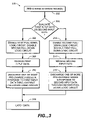
  • FIG. 3 is a flowchart illustrating the operation of the edge-triggered flip-flop of FIG. 2 .
  • FIG. 4 is a schematic diagram an edge-triggered flip-flop including a scan test circuit.
  • FIG. 5 is a schematic diagram an edge-triggered flip-flop including an asynchronous RESET circuit and a scan test circuit.
  • FIG. 2 is a block diagram of an edge-triggered flip-flop 200 .
  • Edge-triggered flip-flop 200 can be any type of edge-triggered flip-flop—e.g., an S-R flip-flop, a J-K flip-flop, a D flip-flop, a T flip-flop, and so on.
  • Edge-triggered flip-flop 200 can be triggered based on a positive and/or negative edge of a clock pulse 202 on a control input of edge-triggered flip-flop 200 .
  • edge-triggered flip-flop 200 includes a pre-charge circuit 204 , a storage circuit 206 , a first pull-down logic circuit 208 , a second pull-down logic circuit 210 , a pull-down enable circuit 212 , and a latch 214 .
  • Pre-charge circuit 204 is in communication with storage circuit 206 and a power supply VDD 218 .
  • Pre-charge circuit 204 can include PMOS (p-channel metal-oxide semiconductor) transistors (not shown) and/or NMOS (n-channel metal-oxide semiconductor) transistors (not shown).
  • pre-charge circuit 204 includes PMOS transistors to pre-charge one or more pre-determined storage nodes in storage circuit 206 to a pre-defined voltage during a pre-charge cycle (as discussed in greater detail below). The duration of the pre-charge cycle can be controlled by a pre-charge clock (not shown).
  • a storage node is a connecting point within a logic circuit to which multiple circuit elements (e.g., transistors) can be coupled.
  • Storage circuit 206 is in communication with first pull-down logic circuit 208 , second pull-down logic circuit 210 , and latch 214 .
  • Latch 214 can store an output value (e.g., output 216 ) of flip-flop 200 .
  • Storage circuit 206 includes one or more pre-determined storage nodes (not shown) operable to store logic states. As discussed above, the one or more pre-determined storage nodes are pre-charged to a pre-defined voltage during a pre-charge cycle.
  • first pull-down logic circuit 208 and second pull-down logic circuit 210 is in communication with storage circuit 206 , a pull-down enable circuit 212 , and a power supply VSS 220 (e.g., ground or a low voltage potential).
  • Each of first pull-down logic circuit 208 and second pull-down logic circuit 210 can perform logic functions—e.g., AND/OR/NOR/NAND/XOR—multiplexer functions, latch functions, asynchronous SET/RESET functions, and so on.
  • first pull-down logic circuit 208 receives as an input first data 222
  • second pull-down logic circuit 210 receives as an input second data 224 .
  • First pull-down logic circuit 208 and second pull-down logic circuit 210 can receive other input signals.
  • First data 222 and second data 224 can be any type of input signal, e.g., operation data, scan chain test data, SET/RESET signals, and so on.
  • First pull-down logic circuit 208 and second pull-down logic circuit 210 provide two separate sense pull-down paths (to VSS 220 ) for discharging one or more pre-charged storage nodes in storage circuit 206 .
  • second pull-down logic circuit 210 is a slower pull-down path relative to first pull-down logic circuit 208 —i.e., second pull-down logic circuit 210 takes a longer time to discharge a pre-charged storage node.
  • Second pull-down logic circuit 210 can include CMOS transistors having a smaller size relative to CMOS transistors in first pull-down logic circuit 208 .
  • first data 222 or second data 224 determines the logic states stored in the one or more storage nodes of storage circuit 206 during an evaluation cycle. If first data 222 is being evaluated, pull-down enable circuit 212 enables first pull-down logic circuit 208 and disables second pull-down logic circuit 210 . If second data 224 is being evaluated, pull-down enable circuit 212 enables second pull-down logic circuit 210 and disables first pull-down logic circuit 208 .
  • FIG. 3 is a flowchart illustrating the operation of edge-triggered flip-flop 200 ( FIG. 2 ).
  • pre-charge circuit 204 pre-charges one or more storage nodes in storage circuit 206 (step 302 ).
  • the storage nodes in storage circuit 206 can be pre-charged to a pre-determined voltage potential (e.g., VDD 218 ).
  • a determination is made whether first data 222 or second data 224 is to be evaluated (step 304 ).
  • first data 222 is received by first pull-down logic circuit 208 (step 308 ).
  • first data 222 includes operation data—i.e., non-test data—for flip-flop 200 .
  • One or more pre-charged storage nodes in storage circuit 206 is discharged through first pull-down logic circuit 208 based on first data 222 (step 310 ).
  • pull-down enable circuit 212 enables second pull-down logic circuit 210 and disables first pull-down logic circuit 208 (step 312 ).
  • Second data 224 is received by second pull-down logic circuit 210 (step 314 ).
  • second data 224 includes test data—e.g., scan chain test data—for testing flip-flop 200 .
  • Input signals other than operation data can also be received by second pull-down logic circuit 210 .
  • second pull-down logic circuit 210 can receive asynchronous SET/RESET inputs.
  • One or more pre-charged storage nodes in storage circuit 206 is discharged through second pull-down logic circuit 210 based on second data 224 (step 316 ).
  • a latch 214 can latch an output value corresponding a logic state of one of the one or more storage nodes (step 318 ).
  • FIG. 4 shows one implementation of flip flop 200 , including pre charge circuit 204 , storage circuit 206 , first pull down logic circuit 208 , second pull down logic circuit 210 , and latch 214 .
  • first pull down logic circuit 208 supports operation logic for flip flop 200
  • second pull-down logic circuit 210 supports a scan chain test circuit for flip flop 200 .
  • Pre charge circuit 204 includes PMOS transistors P 6 P 7 .
  • Storage circuit 206 includes PMOS transistors P 8 –P 9 and NMOS transistors N 6 –N 8 .
  • Storage circuit 206 further includes two storage nodes—i.e., node A and node B. Node A is situated between PMOS transistor P 8 and NMOS transistor N 6 .
  • Node B is situated between PMOS transistor P 9 and NMOS transistor N 7 .
  • node A and node B are complimentary storage nodes operable to store opposite logic states.
  • First pull down logic circuit 208 includes NMOS transistors N 9 –N 12 , and an inverter I 6 .
  • First pull down logic circuit 208 receives as input first data 222 through NMOS transistors N 9 –N 10 .
  • first data 222 is operation data.
  • Second pull down logic circuit 210 includes NMOS transistors N 13 –N 15 , an inverter I 5 , and NOR gates 402 – 404 . Second pull down logic circuit 210 receives as input second data 224 at NOR gate 402 .
  • second data 224 is scan chain test data.
  • Second pull down logic circuit 210 also receives an enable signal 400 that controls NMOS transistor N 12 (of first pull down logic circuit 208 ) and NMOS transistors N 13 N 14 (of second pull down logic circuit 210 ).
  • NMOS transistor N 12 is turned on and NMOS transistors N 13 –N 14 are turned off.
  • First pull-down logic circuit 208 is enabled and second pull-down logic circuit 210 is disabled, i.e., the second sense pull down path of flip-flop 200 is disabled by disabling NMOS transistors N 13 –N 14 .
  • NMOS transistor N 11 is turned off and nodes A and B are pre-charged (e.g., to VDD 218 ) through PMOS transistors P 6 –P 7 . As nodes A and B are pre-charged, NMOS transistors N 6 –N 7 are turned on.
  • pre-charge circuit 204 stops pre-charging nodes A and B
  • NMOS transistor N 11 is turned on.
  • the logic state of nodes A and B are subsequently determined according to first data 222 . For example, if first data 222 is high (or logic state 1 ), NMOS transistor N 9 is turned on and NMOS transistor N 10 is turned off. Once NMOS transistor N 9 is turned on, the pre-charged voltage at node A is discharged through NMOS transistors N 6 , N 9 , N 11 and N 12 (through first pull-down logic circuit 208 ).
  • NMOS transistor N 12 When enable signal 400 is high, NMOS transistor N 12 is turned off, and first pull-down logic circuit 208 is shut off, i.e., the first sense pull down path of flip-flop 200 is disabled.
  • clock pulse 202 When clock pulse 202 is low, NMOS transistor N 15 is turned off and nodes A and B are pre-charged (e.g., to VDD 218 ) through PMOS transistors P 6 –P 7 .
  • pre-charge circuit 204 stops pre-charging nodes A and B, and NMOS transistor N 15 is turned on.
  • the logic state of nodes A and B are subsequently determined according to second data 224 . For example, if second data 224 is high, NOR gate 402 outputs a high voltage potential and NOR gate 404 outputs a low voltage potential. Consequently, NMOS transistor N 13 is turned on and NMOS transistor N 14 is turned off. Once NMOS transistor N 13 is turned on, the pre-charged voltage at node A is discharged through NMOS transistors N 13 and N 15 (of second pull-down logic circuit 210 ).
  • FIG. 5 shows a flip-flop 500 , including pre-charge circuit 204 , storage circuit 206 , first pull-down logic circuit 208 , second pull-down logic circuit 210 , and latch 214 .
  • Flip-flop 500 operates in a similar manner to flip-flop 200 as discussed above with respect to FIG. 4 .
  • second pull-down logic circuit 210 FIG. 5
  • Asynchronous reset circuit 502 includes NAND gate 504 and NOR gate 506 .
  • NAND gate 504 receives RESET data 508 as an input.
  • flip-flop 500 further includes PMOS transistors P 11 –P 13 .
  • PMOS transistors P 11 –P 13 prevent current drive-by—i.e., a direct current path from VDD 218 to VSS 220 through NMOS transistor N 16 .
  • An asynchronous reset operation can occur during the time that clock pulse 202 is high or during the time that clock pulse 202 is low through two different mechanisms.
  • an asynchronous reset operation occurs during the time that clock pulse 206 is high by forcing a low logic state of “0” into storage circuit 206 .
  • NMOS transistor N 13 is turned off and NMOS transistor N 14 is turned on.
  • Node A is charged to a high voltage potential through PMOS transistor P 11 .
  • enable signal 400 goes low, node B is discharged to a low voltage potential through NMOS transistors N 14 –N 15 , thus forcing a low logic state of “0” into storage circuit 206 .
  • PMOS transistors P 12 –P 13 also turn on and cause a low logic state of “0” at output 216 .
  • an asynchronous reset operation occurs during the time that clock pulse 206 is low by forcing data into latch 214 directly through PMOS transistors P 12 –P 13 . Nodes A and B can remain in a pre-charged state during this time.
  • edge-triggered flip-flop 500 can further include a feedback enable signal 510 , as shown in FIG. 5 , to enable edge-triggered flip-flop 500 .
  • feedback enable signal 510 is coupled to input 508 .
  • input 224 functions as an enable signal. That is, when input 224 is high, the data in latch 214 is maintained through feedback enable signal 510 , and when input 224 is low, edge-triggered flip-flop 500 functions normally.
  • FIG. 5 shows flip-flop 500 including an asynchronous RESET function, however, an asynchronous SET function (not shown) can be implemented in a similar manner. Though two separate sense pull-down paths are described above, any number of separate sense pull-down paths can be provided. Accordingly, other implementations are within the scope of the following claims.

Landscapes

  • Logic Circuits (AREA)
  • Tests Of Electronic Circuits (AREA)

Abstract

An edge-triggered flip-flop is provided that includes one or more storage nodes and a pre-charge circuit in communication with the storage circuit. The storage circuit is configured to pre-charge the one or more storage nodes to a pre-determined voltage potential. The storage circuit further includes a first pull-down logic circuit in communication with the storage circuit and separate second pull-down logic circuit in communication with the storage circuit. The first pull-down logic circuit is configured to discharge one or more of the pre-charged storage nodes in response to first input data and the second pull-down logic circuit is configured to discharge one or more of the pre-charged storage nodes in response to second input data.

Description

CROSS-REFERENCE TO RELATED APPLICATIONS
The present application claims priority to commonly assigned U.S. Provisional Patent Application No. 60/533,887, filed on Jan. 2, 2004, which is incorporated herein by reference in its entirety.
BACKGROUND
The following disclosure relates to electrical circuits and signal processing.
A conventional edge-triggered flip-flop is an electronic circuit that can be used as a storage element in logic circuit design. A conventional edge-triggered flip-flop can change state at a positive edge (rising edge) and/or at a negative edge (falling edge) of a clock pulse on a control input of the edge-triggered flip-flop.
Types of edge-triggered flip-flops include, for example, S-R flip-flops, J-K flip-flops, and D flip-flops. Edge-triggered flip-flops include inputs and outputs. Inputs include signal inputs, a SET input, a RESET input, and a clock input. The signal inputs (e.g., S, R, J, K and D) are generally referred to as synchronous inputs of a flip-flop as the signal inputs affect the state of the flip-flop only on the triggering edge of a clock pulse. The SET and RESET inputs are generally referred to as asynchronous inputs as the SET and RESET inputs can affect the state of a flip-flop independent of a clock pulse.
Desirable attributes for an edge-triggered flip-flop include a short setup time, a short clock-to-output delay, and a low capacitance for input signals and the clock signal. Setup time is the time required for input data to be stable before the triggering edge of a clock pulse. Clock-to-output delay is the time required for output data of a flip-flop to be valid after the triggering edge of a clock pulse.
Conventional sense-amp based edge-triggered flip-flops generally have a shorter setup time and a lower input capacitance than conventional master-slave edge-triggered flip-flops in a CMOS (complementary metal-oxide semiconductor) implementation. In addition, the area of a conventional sense-amp based edge-triggered flip-flop is generally comparable to that of a conventional master-slave edge-triggered flip-flop in CMOS implementation.
FIG. 1 shows a conventional sense-amp based, edge-triggered flip-flop, referred to herein as flip-flop 100. Flip-flop 100 includes p-type transistors P1–P5, n-type transistors N1–N5, and inverters I1–I4. Flip-flop 100 further includes transistors T1–T8, that are operable to perform a multiplexing function. Transistors T1–T4 are controlled by input signals S0–S1, and transistors T5–T8 are controlled by input signals D0–D1. Signals S0–S1 are select signals and signals D0–D1 are data input signals. Select signal S0 selects data input signal D0 and select signal S1 selects data input signal D1. In operation, during a pre-charge cycle—i.e., when CLK input 102 is low, complementary storage nodes A and B are pre-charged to VDD. After the pre-charge cycle (when CLK input 102 is high), one of complementary storage nodes A and B is pulled low to VSS according to a selected one of data input signals D0–D1 and value of D0–D1. Flip-flop 100 includes a single sense pull-down path (to VSS) through transistor N4. An output of flip-flop 100 is latched at output 104.
The multiplexing function of transistors T1–T8 can be used to implement a scan chain test. Scan chain testing is a widely used testing scheme for detecting faults of a logic circuit design. Scan chain tests are typically run at low speeds as scan chain tests are primarily used to test stuck-at faults. Transistors T1–T8 can be used to switch input data between operation data (e.g., data input signal D0) and scan data (e.g., data input signal D1), for supporting a scan chain test.
The inclusion of scan chain test functionality (through the multiplexing function of transistors T1–T8), however, degrades the speed performance of flip-flop 100. For example, the setup time of flip-flop 100 increases due to additional delay caused by the 2-to-1 multiplexing function of transistors T1–T8. Furthermore, the input capacitance of flip-flop 100 increases due to the additional transistors required to implement the 2-to-1 multiplexer at the input of flip-flop 100.
Conventional sense-amp based edge-triggered flip-flops typically do not have built-in asynchronous SET/RESET functions, which is another desirable attribute for an edge-triggered flip-flop. Built-in refers to external logic or internal logic implemented with the logic design of a flip-flop. External logic is typically used to implement only synchronous SET/RESET functions in conventional sense-amp based edge-triggered flip-flops.
SUMMARY
In general, in one aspect, this specification describes an edge-triggered flip-flop. The edge-triggered flip-flop includes a storage circuit including one or more storage nodes and a pre-charge circuit in communication with the storage circuit. The storage circuit is configured to pre-charge the one or more storage nodes to a pre-determined voltage potential. The storage circuit further includes a first pull-down logic circuit in communication with the storage circuit and separate second pull-down logic circuit in communication with the storage circuit. The first pull-down logic circuit is configured to discharge one or more of the pre-charged storage nodes in response to first input data and the second pull-down logic circuit is configured to discharge one or more of the pre-charged storage nodes in response to second input data.
Particular implementations can include one or more of the following features. The first pull-down logic circuit can include four transistors. The four transistors of the first pull-down logic circuit can be n-type transistors. The second pull-down logic circuit can include three transistors. The three transistors of the second pull-down logic circuit can be n-type transistors. The edge-triggered flip-flop can further include an enable circuit configured to disable the second pull-down logic circuit while the first pull-down logic circuit is enabled, and disable the first pull-down logic circuit while the second pull-down logic circuit is enabled. The enable circuit can include a first NOR gate and a second NOR gate. The output of the first NOR gate can be an input to the second NOR gate. The second pull-down logic circuit can include a scan chain test circuit configured to receive scan chain test data. The second pull-down logic circuit can include an asynchronous reset circuit configured to asynchronously reset the one or more storage nodes in response to reset data. The asynchronous reset circuit can include a third NOR gate and a first NAND gate.
The edge-triggered flip-flop can further include a latch configured to latch an output value corresponding a logic state of one of the one or more storage nodes. The latch can include two transistors. The two transistors of the latch can be p-type transistors. The edge-triggered flip-flop can be one of an S-R flip-flop, a J-K flip-flop or a D flip-flop. The one or more storage nodes can include two complimentary storage nodes configured to store opposite logic states.
In general, in another aspect, this specification describes an edge-triggered flip-flop that includes a storage circuit means including one or more storage node means and a pre-charge circuit means in communication with the storage circuit means. The storage circuit means is configured to pre-charge the one or more storage node means to a pre-determined voltage potential. The edge-triggered flip-flop further includes a first pull-down logic circuit means in communication with the storage circuit means and a separate second pull-down logic circuit means in communication with the storage circuit means. The first pull-down logic circuit means is configured to discharge one or more of the pre-charged storage node means in response to first input data, and the second pull-down logic circuit means is configured to provide a second path for discharge of one or more of the pre-charged storage node means in response to second input data.
In general, in another aspect, this specification describes a method that includes providing one or more storage nodes in a storage circuit, pre-charging the one or more storage nodes to a pre-determined voltage potential, and discharging one or more of the pre-charged storage nodes through a first pull-down logic circuit in response to first input data or discharging one or more of the pre-charged storage nodes through a separate second pull-down logic circuit in response to second input data.
Particular implementations can include one or more of the following features. The method can further include disabling the second pull-down logic circuit while the first pull-down logic circuit is enabled, and disabling the first pull-down logic circuit while the second pull-down logic circuit is enabled. The method can further include receiving scan chain test data through a scan chain test circuit. The scan chain test circuit can be included within the second pull-down logic circuit. The method can further include asynchronously resetting the one or more storage nodes in response to reset data. The asynchronous reset circuit can be included within the second pull-down logic circuit. The method can further include latching an output value corresponding a logic state of one of the one or more storage nodes. The method can further include storing opposite logic states within the one or more storage nodes.
Implementations can include one or more of the following advantages. An edge-triggered flip-flop is provided that includes two separate sense pull-down paths for sensing separate data inputs. One sense pull-down path can be used to sense operation data, and the second sense pull-down path can be used to sense other data inputs (e.g., scan chain test data, SET/RESET data, and so on). The second sense pull-down path is isolated from the first sense pull-down path—i.e., the second sense pull-down path is disabled while the first sense pull-down path is enabled, and vice-versa. By providing isolation of the first sense pull-down path from the second sense pull-down path, there is no performance degradation with respect to normal operation of the edge-triggered flip-flop, and the flip-flop maintains a short setup time and a short clock-to-output delay (e.g., 30–50 picoseconds). In addition, in one implementation, an edge-triggered flip-flop is provided that includes built-in SET/RESET functions.
The details of one or more implementations are set forth in the accompanying drawings and the description below. Other features and advantages will be apparent from the description and drawings, and from the claims.
DESCRIPTION OF DRAWINGS
FIG. 1 is a schematic diagram of a conventional edge-triggered flip-flop.
FIG. 2 is block diagram of an edge-triggered flip-flop.
FIG. 3 is a flowchart illustrating the operation of the edge-triggered flip-flop of FIG. 2.
FIG. 4 is a schematic diagram an edge-triggered flip-flop including a scan test circuit.
FIG. 5 is a schematic diagram an edge-triggered flip-flop including an asynchronous RESET circuit and a scan test circuit.
Like reference symbols in the various drawings indicate like elements.
DETAILED DESCRIPTION
FIG. 2 is a block diagram of an edge-triggered flip-flop 200. Edge-triggered flip-flop 200 can be any type of edge-triggered flip-flop—e.g., an S-R flip-flop, a J-K flip-flop, a D flip-flop, a T flip-flop, and so on. Edge-triggered flip-flop 200 can be triggered based on a positive and/or negative edge of a clock pulse 202 on a control input of edge-triggered flip-flop 200. In one implementation, edge-triggered flip-flop 200 includes a pre-charge circuit 204, a storage circuit 206, a first pull-down logic circuit 208, a second pull-down logic circuit 210, a pull-down enable circuit 212, and a latch 214.
Pre-charge circuit 204 is in communication with storage circuit 206 and a power supply VDD 218. Pre-charge circuit 204 can include PMOS (p-channel metal-oxide semiconductor) transistors (not shown) and/or NMOS (n-channel metal-oxide semiconductor) transistors (not shown). In one implementation, pre-charge circuit 204 includes PMOS transistors to pre-charge one or more pre-determined storage nodes in storage circuit 206 to a pre-defined voltage during a pre-charge cycle (as discussed in greater detail below). The duration of the pre-charge cycle can be controlled by a pre-charge clock (not shown). A storage node is a connecting point within a logic circuit to which multiple circuit elements (e.g., transistors) can be coupled.
Storage circuit 206 is in communication with first pull-down logic circuit 208, second pull-down logic circuit 210, and latch 214. Latch 214 can store an output value (e.g., output 216) of flip-flop 200. Storage circuit 206 includes one or more pre-determined storage nodes (not shown) operable to store logic states. As discussed above, the one or more pre-determined storage nodes are pre-charged to a pre-defined voltage during a pre-charge cycle.
Each of first pull-down logic circuit 208 and second pull-down logic circuit 210 is in communication with storage circuit 206, a pull-down enable circuit 212, and a power supply VSS 220 (e.g., ground or a low voltage potential). Each of first pull-down logic circuit 208 and second pull-down logic circuit 210 can perform logic functions—e.g., AND/OR/NOR/NAND/XOR—multiplexer functions, latch functions, asynchronous SET/RESET functions, and so on. In one implementation, first pull-down logic circuit 208 receives as an input first data 222, and second pull-down logic circuit 210 receives as an input second data 224. First pull-down logic circuit 208 and second pull-down logic circuit 210 can receive other input signals. First data 222 and second data 224 can be any type of input signal, e.g., operation data, scan chain test data, SET/RESET signals, and so on.
First pull-down logic circuit 208 and second pull-down logic circuit 210 provide two separate sense pull-down paths (to VSS 220) for discharging one or more pre-charged storage nodes in storage circuit 206. In one implementation, second pull-down logic circuit 210 is a slower pull-down path relative to first pull-down logic circuit 208—i.e., second pull-down logic circuit 210 takes a longer time to discharge a pre-charged storage node. Second pull-down logic circuit 210 can include CMOS transistors having a smaller size relative to CMOS transistors in first pull-down logic circuit 208.
One of first data 222 or second data 224 determines the logic states stored in the one or more storage nodes of storage circuit 206 during an evaluation cycle. If first data 222 is being evaluated, pull-down enable circuit 212 enables first pull-down logic circuit 208 and disables second pull-down logic circuit 210. If second data 224 is being evaluated, pull-down enable circuit 212 enables second pull-down logic circuit 210 and disables first pull-down logic circuit 208.
FIG. 3 is a flowchart illustrating the operation of edge-triggered flip-flop 200 (FIG. 2). Referring to FIGS. 2 and 3, pre-charge circuit 204 pre-charges one or more storage nodes in storage circuit 206 (step 302). The storage nodes in storage circuit 206 can be pre-charged to a pre-determined voltage potential (e.g., VDD 218). A determination is made whether first data 222 or second data 224 is to be evaluated (step 304).
If first data 222 is to be evaluated, then pull-down enable circuit 212 enables first pull-down logic circuit 208 and disables second pull-down logic circuit 210 (step 306). First data 222 is received by first pull-down logic circuit 208 (step 308). In one implementation, first data 222 includes operation data—i.e., non-test data—for flip-flop 200. One or more pre-charged storage nodes in storage circuit 206 is discharged through first pull-down logic circuit 208 based on first data 222 (step 310). If second data 224 is to be evaluated, then pull-down enable circuit 212 enables second pull-down logic circuit 210 and disables first pull-down logic circuit 208 (step 312). Second data 224 is received by second pull-down logic circuit 210 (step 314). In one implementation, second data 224 includes test data—e.g., scan chain test data—for testing flip-flop 200. Input signals other than operation data can also be received by second pull-down logic circuit 210. For example, second pull-down logic circuit 210 can receive asynchronous SET/RESET inputs. One or more pre-charged storage nodes in storage circuit 206 is discharged through second pull-down logic circuit 210 based on second data 224 (step 316). A latch 214 can latch an output value corresponding a logic state of one of the one or more storage nodes (step 318).
FIG. 4 shows one implementation of flip flop 200, including pre charge circuit 204, storage circuit 206, first pull down logic circuit 208, second pull down logic circuit 210, and latch 214. In the implementation of FIG. 4, first pull down logic circuit 208 supports operation logic for flip flop 200 and second pull-down logic circuit 210 supports a scan chain test circuit for flip flop 200. Pre charge circuit 204 includes PMOS transistors P6 P7. Storage circuit 206 includes PMOS transistors P8–P9 and NMOS transistors N6–N8. Storage circuit 206 further includes two storage nodes—i.e., node A and node B. Node A is situated between PMOS transistor P8 and NMOS transistor N6. Node B is situated between PMOS transistor P9 and NMOS transistor N7. In one implementation, node A and node B are complimentary storage nodes operable to store opposite logic states. First pull down logic circuit 208 includes NMOS transistors N9–N12, and an inverter I6. First pull down logic circuit 208 receives as input first data 222 through NMOS transistors N9–N10. In one implementation, first data 222 is operation data. Second pull down logic circuit 210 includes NMOS transistors N13–N15, an inverter I5, and NOR gates 402404. Second pull down logic circuit 210 receives as input second data 224 at NOR gate 402. In one implementation, second data 224 is scan chain test data. Second pull down logic circuit 210 also receives an enable signal 400 that controls NMOS transistor N12 (of first pull down logic circuit 208) and NMOS transistors N13 N14 (of second pull down logic circuit 210).
In operation, when enable signal 400 is low, the outputs of NOR gates 402404 are low. NMOS transistor N12 is turned on and NMOS transistors N13–N14 are turned off. First pull-down logic circuit 208 is enabled and second pull-down logic circuit 210 is disabled, i.e., the second sense pull down path of flip-flop 200 is disabled by disabling NMOS transistors N13–N14. During the time that the second pull-down logic circuit 210 is disabled and when clock pulse 202 is low (which indicates a pre-charge cycle), NMOS transistor N11 is turned off and nodes A and B are pre-charged (e.g., to VDD 218) through PMOS transistors P6–P7. As nodes A and B are pre-charged, NMOS transistors N6–N7 are turned on.
After the pre-charge cycle—i.e., when clock pulse 202 goes high—PMOS transistors P6–P7 are turned off (pre-charge circuit 204 stops pre-charging nodes A and B) and NMOS transistor N11 is turned on. The logic state of nodes A and B are subsequently determined according to first data 222. For example, if first data 222 is high (or logic state 1), NMOS transistor N9 is turned on and NMOS transistor N10 is turned off. Once NMOS transistor N9 is turned on, the pre-charged voltage at node A is discharged through NMOS transistors N6, N9, N11 and N12 (through first pull-down logic circuit 208). When the voltage potential at node A goes low (or logic state 0), PMOS transistor P9 turns on and NMOS transistor N7 turns off. A high voltage potential, therefore, remains at node B. The low voltage potential at node A is provided to inverter I7 and turns on NMOS transistor N16, and a high voltage potential is output at output 216. Output 216 is high when first data 222 is high. Conversely, output 216 is low when first data 222 is low.
When enable signal 400 is high, NMOS transistor N12 is turned off, and first pull-down logic circuit 208 is shut off, i.e., the first sense pull down path of flip-flop 200 is disabled. When clock pulse 202 is low, NMOS transistor N15 is turned off and nodes A and B are pre-charged (e.g., to VDD 218) through PMOS transistors P6–P7.
After the pre-charge cycle—i.e., when clock pulse 202 goes high, pre-charge circuit 204 stops pre-charging nodes A and B, and NMOS transistor N15 is turned on. The logic state of nodes A and B are subsequently determined according to second data 224. For example, if second data 224 is high, NOR gate 402 outputs a high voltage potential and NOR gate 404 outputs a low voltage potential. Consequently, NMOS transistor N13 is turned on and NMOS transistor N14 is turned off. Once NMOS transistor N13 is turned on, the pre-charged voltage at node A is discharged through NMOS transistors N13 and N15 (of second pull-down logic circuit 210). When the voltage potential at node A goes low (or logic state 0), PMOS transistor P9 turns on and NMOS transistor N7 turns off. A high voltage potential, therefore, remains at node B. As discussed in the example above, the low voltage potential at node A is provided to inverter I7 and turns on NMOS transistor N16, and a high voltage potential is output at output 216. Output 216 is high when second data 224 is high. Conversely, output 216 is low when second data 224 is low.
FIG. 5 shows a flip-flop 500, including pre-charge circuit 204, storage circuit 206, first pull-down logic circuit 208, second pull-down logic circuit 210, and latch 214. Flip-flop 500 operates in a similar manner to flip-flop 200 as discussed above with respect to FIG. 4. However, second pull-down logic circuit 210 (FIG. 5) further includes a built-in asynchronous reset circuit 502 for performing RESET functions. Asynchronous reset circuit 502 includes NAND gate 504 and NOR gate 506. NAND gate 504 receives RESET data 508 as an input. In one implementation, flip-flop 500 further includes PMOS transistors P11–P13. PMOS transistors P11–P13 prevent current drive-by—i.e., a direct current path from VDD 218 to VSS 220 through NMOS transistor N16.
An asynchronous reset operation can occur during the time that clock pulse 202 is high or during the time that clock pulse 202 is low through two different mechanisms.
In one implementation, an asynchronous reset operation occurs during the time that clock pulse 206 is high by forcing a low logic state of “0” into storage circuit 206. Based on RESET data 508 and enable signal 400, NMOS transistor N13 is turned off and NMOS transistor N14 is turned on. Node A is charged to a high voltage potential through PMOS transistor P11. When enable signal 400 goes low, node B is discharged to a low voltage potential through NMOS transistors N14–N15, thus forcing a low logic state of “0” into storage circuit 206. PMOS transistors P12–P13 also turn on and cause a low logic state of “0” at output 216.
In one implementation, an asynchronous reset operation occurs during the time that clock pulse 206 is low by forcing data into latch 214 directly through PMOS transistors P12–P13. Nodes A and B can remain in a pre-charged state during this time.
A number of implementations have been described. Nevertheless, it will be understood that various modifications may be made without departing from the spirit and scope of the invention. For example, edge-triggered flip-flop 500 can further include a feedback enable signal 510, as shown in FIG. 5, to enable edge-triggered flip-flop 500. In one implementation, feedback enable signal 510 is coupled to input 508. In this implementation, input 224 functions as an enable signal. That is, when input 224 is high, the data in latch 214 is maintained through feedback enable signal 510, and when input 224 is low, edge-triggered flip-flop 500 functions normally. In addition, FIG. 5 shows flip-flop 500 including an asynchronous RESET function, however, an asynchronous SET function (not shown) can be implemented in a similar manner. Though two separate sense pull-down paths are described above, any number of separate sense pull-down paths can be provided. Accordingly, other implementations are within the scope of the following claims.

Claims (47)

1. An edge-triggered flip-flop, comprising:
a storage circuit including one or more storage nodes;
a pre-charge circuit in communication with the storage circuit, the storage circuit configured to pre-charge the one or more storage nodes to a pre-determined voltage potential;
a first pull-down logic circuit in communication with the storage circuit, the first pull-down logic circuit configured to provide a first path for discharge of one or more of the pre-charged storage nodes in response to first input data; and
a separate second pull-down logic circuit in communication with the storage circuit, the second pull-down logic circuit configured to provide a second path for discharge of one or more of the pre-charged storage nodes in response to second input data.
2. The edge-triggered flip-flop of claim 1, wherein the first pull-down logic circuit comprises four transistors.
3. The edge-triggered flip-flop of claim 2, wherein the four transistors of the first pull-down logic circuit are n-type transistors.
4. The edge-triggered flip-flop of claim 1, wherein the second pull-down logic circuit comprises three transistors.
5. The edge-triggered flip-flop of claim 4, wherein the three transistors of the second pull-down logic circuit are n-type transistors.
6. The edge-triggered flip-flop of claim 1, further comprising:
an enable circuit configured to disable the second pull-down logic circuit while the first pull-down logic circuit is enabled, and configured to disable the first pull-down logic circuit while the second pull-down logic circuit is enabled.
7. The edge-triggered flip-flop of claim 6, wherein the enable circuit comprises a first NOR gate and a second NOR gate.
8. The edge-triggered flip-flop of claim 7, wherein the output of the first NOR gate is an input to the second NOR gate.
9. The edge-triggered flip-flop of claim 1, wherein the second pull-down logic circuit includes a scan chain test circuit configured to receive scan chain test data.
10. The edge-triggered flip-flop of claim 1, wherein the second pull-down logic circuit includes an asynchronous reset circuit configured to asynchronously reset the one or more storage nodes in response to reset data.
11. The edge-triggered flip-flop of claim 10, wherein the asynchronous reset circuit comprises a third NOR gate and a first NAND gate.
12. The edge-triggered flip-flop of claim 1, further comprising a latch configured to latch an output value corresponding a logic state of one of the one or more storage nodes.
13. The edge-triggered flip-flop of claim 12, wherein the latch comprises two transistors.
14. The edge-triggered flip-flop of claim 13, wherein the two transistors of the latch are p-type transistors.
15. The edge-triggered flip-flop of claim 1, wherein the edge-triggered flip-flop is one of an S-R flip-flop, a J-K flip-flop or a D flip-flop.
16. The edge-triggered flip-flop of claim 1, wherein the one or more storage nodes include two complimentary storage nodes configured to store opposite logic states.
17. The edge-triggered flip-flop of claim 1, wherein the first pull-down logic circuit discharges one or more of the pre-charged storage nodes in response to only the first input data, and the second pull-down logic circuit discharges one or more of the pre-charged storage nodes in response to only the second input data.
18. The edge-triggered flip-flop of claim 1, wherein the first pull-down logic circuit is adapted to be operated independently from the second pull-down logic circuit.
19. The edge-triggered flip-flop of claim 1, wherein each of the first pull-down logic circuit and the second pull-down logic circuit discharges two or more of the pre-charged storage nodes.
20. An edge-triggered flip-flop, comprising:
a storage circuit means including one or more storage node means;
a pre-charge circuit means in communication with the storage circuit means, the storage circuit means configured to pre-charge the one or more storage node means to a pre-determined voltage potential;
a first pull-down logic circuit means in communication with the storage circuit means, the first pull-down logic circuit means configured to provide a first path for discharge of one or more of the pre-charged storage node means in response to first input data; and
a separate second pull-down logic circuit means in communication with the storage circuit means, the second pull-down logic circuit means configured to provide a second path for discharge of one or more of the pre-charged storage node means in response to second input data.
21. The edge-triggered flip-flop of claim 20, wherein the first pull-down logic circuit means comprises four transistor means.
22. The edge-triggered flip-flop of claim 21, wherein the four transistor means of the first pull-down logic circuit means are n-type transistor means.
23. The edge-triggered flip-flop of claim 20, wherein the second pull-down logic circuit means comprises three transistor means.
24. The edge-triggered flip-flop of claim 23, wherein the three transistor means of the second pull-down logic circuit means are n-type transistor means.
25. The edge-triggered flip-flop of claim 20, further comprising:
enable circuit means configured to disable the second pull-down logic circuit means while the first pull-down logic circuit means is enabled, and configured to disable the first pull-down logic circuit means while the second pull-down logic circuit means is enabled.
26. The edge-triggered flip-flop of claim 25, wherein the enable circuit means comprises a first NOR gate means and a second NOR gate means.
27. The edge-triggered flip-flop of claim 26, wherein the output of the first NOR gate means is an input to the second NOR gate means.
28. The edge-triggered flip-flop of claim 20, wherein the second pull-down logic circuit means includes a scan chain test circuit means configured to receive scan chain test data.
29. The edge-triggered flip-flop of claim 20, wherein the second pull-down logic circuit means includes an asynchronous reset circuit means configured to asynchronously reset the one or more storage node means in response to reset data.
30. The edge-triggered flip-flop of claim 29, wherein the asynchronous reset circuit means comprises a third NOR gate means and a first NAND gate means.
31. The edge-triggered flip-flop of claim 20, further comprising latch means configured to latch an output value corresponding a logic state of one of the one or more storage node means.
32. The edge-triggered flip-flop of claim 31, wherein the latch means comprises two transistor means.
33. The edge-triggered flip-flop of claim 32, wherein the two transistor means of the latch means are p-type transistor means.
34. The edge-triggered flip-flop of claim 20, wherein the edge-triggered flip-flop is one of an S-R flip-flop means, a J-K flip-flop means or a D flip-flop means.
35. The edge-triggered flip-flop of claim 20, wherein the one or more storage node means include two complimentary storage node means configured to store opposite logic states.
36. The edge-triggered flip-flop of claim 20, wherein the first pull-down logic circuit means discharges one or more of the pre-charged storage node means in response to only the first input data, and the second pull-down logic circuit means discharges one or more of the pre-charged storage node means in response to only the second input data.
37. The edge-triggered flip-flop of claim 20, wherein the first pull-down logic circuit means is adapted to be operated independently from the second pull-down logic circuit means.
38. The edge-triggered flip-flop of claim 20, wherein each of the first pull-down logic circuit means and the second pull-down logic circuit means discharges two or more of the pre-charged storage node means.
39. A method, comprising:
providing one or more storage nodes in a storage circuit;
pre-charging the one or more storage nodes to a pre-determined voltage potential; and
discharging one or more of the pre-charged storage nodes through a first pull-down logic circuit in response to first input data or discharging one or more of the pre-charged storage nodes through a separate second pull-down logic circuit providing a first path, providing a second path, in response to second input data.
40. The method of claim 39, further comprising:
disabling the second pull-down logic circuit while the first pull-down logic circuit is enabled, and disabling the first pull-down logic circuit while the second pull-down logic circuit is enabled.
41. The method of claim 39, further comprising receiving scan chain test data through a scan chain test circuit within the second pull-down logic circuit.
42. The method of claim 39, further comprising asynchronously resetting the one or more storage nodes in response to reset data.
43. The method of claim 39, further comprising latching an output value corresponding a logic state of one of the one or more storage nodes.
44. The method of claim 39, further comprising storing opposite logic states within the one or more storage nodes.
45. The method of claim 39, further comprising discharging one or more of the precharged storage nodes using the first pull-down logic circuit in response to only the first input data, and discharging one or more of the pre-charged storage nodes using the second pull-down logic circuit in response to only the second input data.
46. The method of claim 39, further comprising adapting the first pull-down logic circuit to be operated independently from the second pull-down logic circuit.
47. The method of claim 39, wherein discharging one or more of the pre-charged storage nodes includes discharging two or more of the pre-charged storage nodes using the first pull-down logic circuit and discharging two or more of the pre-charged storage nodes using the second pull-down logic circuit.
US10/851,048 2004-01-02 2004-05-21 Edge-triggered flip-flop Expired - Fee Related US7242234B1 (en)

Priority Applications (1)

Application Number Priority Date Filing Date Title
US10/851,048 US7242234B1 (en) 2004-01-02 2004-05-21 Edge-triggered flip-flop

Applications Claiming Priority (2)

Application Number Priority Date Filing Date Title
US53388704P 2004-01-02 2004-01-02
US10/851,048 US7242234B1 (en) 2004-01-02 2004-05-21 Edge-triggered flip-flop

Publications (1)

Publication Number Publication Date
US7242234B1 true US7242234B1 (en) 2007-07-10

Family

ID=38227052

Family Applications (1)

Application Number Title Priority Date Filing Date
US10/851,048 Expired - Fee Related US7242234B1 (en) 2004-01-02 2004-05-21 Edge-triggered flip-flop

Country Status (1)

Country Link
US (1) US7242234B1 (en)

Cited By (1)

* Cited by examiner, † Cited by third party
Publication number Priority date Publication date Assignee Title
JP2018063745A (en) * 2016-10-04 2018-04-19 ローム株式会社 Data holding device, non-volatile data holding device, and data reading method

Citations (2)

* Cited by examiner, † Cited by third party
Publication number Priority date Publication date Assignee Title
US6070259A (en) * 1998-01-15 2000-05-30 Lsi Logic Corporation Dynamic logic element having non-invasive scan chain insertion
US6388471B1 (en) 2000-05-12 2002-05-14 Sandcraft, Inc. Single phase edge trigger register

Patent Citations (2)

* Cited by examiner, † Cited by third party
Publication number Priority date Publication date Assignee Title
US6070259A (en) * 1998-01-15 2000-05-30 Lsi Logic Corporation Dynamic logic element having non-invasive scan chain insertion
US6388471B1 (en) 2000-05-12 2002-05-14 Sandcraft, Inc. Single phase edge trigger register

Cited By (1)

* Cited by examiner, † Cited by third party
Publication number Priority date Publication date Assignee Title
JP2018063745A (en) * 2016-10-04 2018-04-19 ローム株式会社 Data holding device, non-volatile data holding device, and data reading method

Similar Documents

Publication Publication Date Title
US8656238B2 (en) Flip-flop circuit and scan flip-flop circuit
US7859310B2 (en) Semiconductor integrated circuit
US10049726B1 (en) Contention-free dynamic logic
KR20090099735A (en) Flip-flop for high speed operation
US7719319B2 (en) Semiconductor integrated circuit
US7595665B2 (en) Clock gated circuit
US7161390B2 (en) Dynamic latching logic structure with static interfaces for implementing improved data setup time
US20040140835A1 (en) Multiple trip point fuse latch device and method
US8824215B2 (en) Data storage circuit that retains state during precharge
US8928377B2 (en) Scannable fast dynamic register
TWI508450B (en) Semi-dynamic flip-flop
US11545964B2 (en) High speed flipflop circuit
US7961009B2 (en) Domino logic block having data holding function and domino logic including the domino logic block
US20080084235A1 (en) Dynamic scannable latch and method of operation
US7242234B1 (en) Edge-triggered flip-flop
US7164293B2 (en) Dynamic latch having integral logic function and method therefor
US8432195B2 (en) Latch circuits with synchronous data loading and self-timed asynchronous data capture
US8330588B2 (en) Fast repeater latch
US6388471B1 (en) Single phase edge trigger register
KR100400042B1 (en) Complementary Pass transistor based Flip Flop
US20100164549A1 (en) Logic gate
GB2437439A (en) A pulse-type flip-flop using a latch with clocked inverters

Legal Events

Date Code Title Description
AS Assignment

Owner name: MARVELL INTERNATIONAL LTD., BERMUDA

Free format text: ASSIGNMENT OF ASSIGNORS INTEREST;ASSIGNOR:MARVELL SEMICONDUCTOR, INC.;REEL/FRAME:015382/0738

Effective date: 20040521

Owner name: MARVELL SEMICONDUCTOR, INC., CALIFORNIA

Free format text: ASSIGNMENT OF ASSIGNORS INTEREST;ASSIGNOR:LU, WEI-PING;REEL/FRAME:015382/0796

Effective date: 20040521

STCF Information on status: patent grant

Free format text: PATENTED CASE

FPAY Fee payment

Year of fee payment: 4

FPAY Fee payment

Year of fee payment: 8

FEPP Fee payment procedure

Free format text: MAINTENANCE FEE REMINDER MAILED (ORIGINAL EVENT CODE: REM.); ENTITY STATUS OF PATENT OWNER: LARGE ENTITY

LAPS Lapse for failure to pay maintenance fees

Free format text: PATENT EXPIRED FOR FAILURE TO PAY MAINTENANCE FEES (ORIGINAL EVENT CODE: EXP.); ENTITY STATUS OF PATENT OWNER: LARGE ENTITY

STCH Information on status: patent discontinuation

Free format text: PATENT EXPIRED DUE TO NONPAYMENT OF MAINTENANCE FEES UNDER 37 CFR 1.362

FP Lapsed due to failure to pay maintenance fee

Effective date: 20190710