US7242231B2 - Programmable fractional-N clock generators - Google Patents
Programmable fractional-N clock generators Download PDFInfo
- Publication number
- US7242231B2 US7242231B2 US11/232,949 US23294905A US7242231B2 US 7242231 B2 US7242231 B2 US 7242231B2 US 23294905 A US23294905 A US 23294905A US 7242231 B2 US7242231 B2 US 7242231B2
- Authority
- US
- United States
- Prior art keywords
- clock
- clocks
- frequency
- phase
- output
- Prior art date
- Legal status (The legal status is an assumption and is not a legal conclusion. Google has not performed a legal analysis and makes no representation as to the accuracy of the status listed.)
- Expired - Fee Related, expires
Links
Images


Classifications
-
- H—ELECTRICITY
- H03—ELECTRONIC CIRCUITRY
- H03L—AUTOMATIC CONTROL, STARTING, SYNCHRONISATION, OR STABILISATION OF GENERATORS OF ELECTRONIC OSCILLATIONS OR PULSES
- H03L7/00—Automatic control of frequency or phase; Synchronisation
- H03L7/06—Automatic control of frequency or phase; Synchronisation using a reference signal applied to a frequency- or phase-locked loop
- H03L7/08—Details of the phase-locked loop
- H03L7/099—Details of the phase-locked loop concerning mainly the controlled oscillator of the loop
- H03L7/0995—Details of the phase-locked loop concerning mainly the controlled oscillator of the loop the oscillator comprising a ring oscillator
-
- H—ELECTRICITY
- H03—ELECTRONIC CIRCUITRY
- H03K—PULSE TECHNIQUE
- H03K5/00—Manipulating of pulses not covered by one of the other main groups of this subclass
- H03K5/13—Arrangements having a single output and transforming input signals into pulses delivered at desired time intervals
- H03K5/133—Arrangements having a single output and transforming input signals into pulses delivered at desired time intervals using a chain of active delay devices
-
- H—ELECTRICITY
- H03—ELECTRONIC CIRCUITRY
- H03L—AUTOMATIC CONTROL, STARTING, SYNCHRONISATION, OR STABILISATION OF GENERATORS OF ELECTRONIC OSCILLATIONS OR PULSES
- H03L7/00—Automatic control of frequency or phase; Synchronisation
- H03L7/06—Automatic control of frequency or phase; Synchronisation using a reference signal applied to a frequency- or phase-locked loop
- H03L7/16—Indirect frequency synthesis, i.e. generating a desired one of a number of predetermined frequencies using a frequency- or phase-locked loop
-
- H—ELECTRICITY
- H03—ELECTRONIC CIRCUITRY
- H03K—PULSE TECHNIQUE
- H03K5/00—Manipulating of pulses not covered by one of the other main groups of this subclass
- H03K2005/00013—Delay, i.e. output pulse is delayed after input pulse and pulse length of output pulse is dependent on pulse length of input pulse
- H03K2005/00019—Variable delay
- H03K2005/00058—Variable delay controlled by a digital setting
- H03K2005/00065—Variable delay controlled by a digital setting by current control, e.g. by parallel current control transistors
Definitions
- the invention relates to clock generators, and more particularly, to clock generators capable of generating clocks with different frequency according to a binary code.
- Fractional-N (% N) clock generators are widely applied to microprocessors and communication systems.
- the conventional fractional-N clock generators however, not only have jitters and inaccuracy in their duty cycle but also require a large chip area.
- a voltage controlled oscillation module generates a plurality of first clocks (D 0 ⁇ D m ) with a first frequency (f 0 ), in which the first clocks D i and D i-1 have a fixed phase difference and 1 ⁇ i ⁇ m.
- a logic control circuit outputs a set of corresponding clocks arranged by a corresponding sequence according to the first clocks and a binary code.
- a clock synthesizer generates a second clock with a second frequency (f 1 ) according to the set of corresponding clocks, in which
- f ⁇ ⁇ 1 A B ⁇ f ⁇ ⁇ 0 , A ⁇ B and A and B are positive integers.
- the invention also discloses embodiments of phase-locked loops, in which a voltage controlled oscillation module generates a plurality of first clocks (D 0 ⁇ D m ) with a first frequency (f 0 ), wherein the first clocks D i and D i-1 have a fixed phase difference and 1 ⁇ i ⁇ m.
- a logic control circuit outputs a set of corresponding clocks arranged by a corresponding sequence according to the first clocks and a binary code.
- a clock synthesizer generates a second clock with a second frequency (f 1 ) according to the set of corresponding clocks, wherein
- a phase-frequency detector generates a control signal according to a phase difference between the second clock and a reference clock.
- a charge pump receives the control signal and generates a control voltage by a low pass filter to control the voltage controlled oscillation module.
- the invention also discloses embodiments of clock generation methods, in which a plurality of first clocks (D 0 ⁇ Dm) with a first frequency (f 0 ) is generated, wherein the first clocks D i and D i-1 have a fixed phase difference and 1 ⁇ i ⁇ m.
- a set of corresponding clocks arranged by a corresponding sequence is output according to the first clocks and a binary code.
- a second clock with a second frequency (f 1 ) is synthesized according to the set of corresponding clocks, wherein
- f ⁇ ⁇ 1 A B ⁇ f ⁇ ⁇ 0 , A ⁇ B and A and B are positive integers.
- FIG. 1A shows an embodiment of a clock generator
- FIG. 1B shows another embodiment of the clock generator
- FIG. 2 shows an embodiment of a voltage controlled oscillation module
- FIG. 3 is a timing chart of the clocks output from the voltage controlled oscillation module
- FIG. 4A shows an embodiment of a logic control circuit
- FIG. 4B shows another embodiment of the logic control circuit
- FIG. 5A shows an embodiment of a clock synthesizer
- FIG. 5B shows another embodiment of the clock synthesizer
- FIG. 6 is a timing chart of the clock synthesizer
- FIG. 7 shows an embodiment of the true single-phase circuit (TSPC).
- FIGS. 8A ⁇ 8D are output waves of the clock generator shown in FIG. 1A under different binary codes
- FIG. 9 shows an embodiment of an output control circuit
- FIG. 10 is output wave of the clock generator shown in FIG. 1B under different binary codes
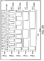
- FIG. 11 is a relational table of the duty cycle and time of the clock generator.
- FIG. 12 shows an embodiment of a phase locked loop.
- FIG. 1A shows an embodiment of a clock generator.
- the clock generator 100 A comprises a voltage controlled oscillation module 10 , a logic control circuit 20 , a clock synthesizer 30 and a frequency divider 40 A.
- the voltage controlled oscillation module 10 generates a plurality of clocks d 1 ⁇ d 8 with a first frequency (f 0 ). In clocks d 1 ⁇ d 8 , there is a fixed phase difference phase between each clock and the next clock.
- the logic control circuit 20 outputs a set of corresponding clocks arranged by a corresponding sequence according to the clocks d 1 ⁇ d 8 and a binary code.
- the binary code can be a four-bit code (in 1 ⁇ in 4 ), but it is to be understood that the invention is not limited thereto.
- the logic control circuit 20 also generates a control signal S 0 and outputs to the frequency divider 40 A according to the binary code in 1 ⁇ in 4 .
- the voltage controlled oscillation module 10 for example, can be a phase-locked loop (PLL).
- the clock synthesizer 30 is coupled to the logic control circuit 20 to generate a clock C 1 with a second frequency (f 1 ) according to the set of corresponding clocks from the logic control circuit 20 , in which
- the frequency divider 40 A selectively receives the clock C 1 from the clock synthesizer 30 or the clock d 1 from the voltage controlled oscillation module 10 according to the control signal S 0 from the logic control circuit 20 .
- the frequency divider 40 A divides the received clock (C 1 or d 1 ) by 2 N and outputs the divided clock, in which N is positive integer and N>1.
- frequency divider 40 A comprises three true single-phase circuits (TSPC) 42 A ⁇ 42 C connected in series, but it is to be understood that the invention is not limited thereto.
- the TSPC 42 A When the frequency divider 40 A receives the clock C 1 with a frequency f 1 from the clock synthesizer 30 , the TSPC 42 A outputs a clock C 2 with a frequency of
- the TSPC 42 B outputs a clock C 3 with a frequency of
- the TSPC 42 A When the frequency divider 40 A receives the clock d 1 with the frequency f 0 from the voltage controlled oscillation module 10 , the TSPC 42 A outputs a clock C 2 with a frequency of
- the TSPC 42 B outputs a clock C 3 with a frequency of
- FIG. 2 shows an embodiment of a voltage controlled oscillation module.
- the voltage controlled oscillation module comprises 4 stages of voltage controlled oscillators connected in series, generating clocks d 1 ⁇ d 8 with the same frequency.
- FIG. 3 is a timing chart of the clocks output from the voltage controlled oscillation module. As shown, in clocks d 1 ⁇ d 8 , there is a fixed phase difference between the each clock and the next clock. For example, there is a phase difference of 45° between the clocks d 1 and d 2 , between the clocks d 2 and d 3 , and so on.
- FIG. 4A shows an embodiment of a logic control circuit.
- the logic control circuit 20 A comprises three transfer units 22 A ⁇ 22 C and a logic unit 24 A.
- the logic unit 24 A comprises three AND gates AD 1 ⁇ AD 3 , five inverters INV 5 ⁇ INV 9 and a NOR gate XD 1 , generating control signals a, b, c and S 0 according to the binary code in 1 ⁇ in 4 .
- the transfer units 22 A ⁇ 22 C each comprise eight AND gates and a switch unit comprising eight transmission gates (not shown), outputting the received clock according to the control signal a, b and c from the transfer unit 22 A.
- Input terminals of the transfer unit 22 A are coupled to the clocks d 1 , d 7 , d 5 , d 3 , d 1 , d 7 , d 5 and d 3 respectively
- input terminals of the transfer unit 22 B are coupled to the clocks d 1 , d 6 , d 3 , d 8 , d 5 , d 2 , d 7 and d 4 respectively
- input terminals of the transfer unit 22 C are coupled to the clocks d 1 , d 8 , d 7 , d 6 , d 5 , d 4 , d 3 and d 2 respectively.
- the transfer units 22 A ⁇ 22 C receive clocks d 1 ⁇ d 8 from the voltage controlled oscillation module 10 , and output clocks arranged in a different sequence.
- the transfer unit 22 A outputs clocks arranged in a first sequence (d 1 ⁇ d 7 ⁇ d 5 ⁇ d 3 ⁇ d 1 ⁇ d 7 ⁇ d 5 ⁇ d 3 )
- the transfer unit 22 B outputs clocks arranged in a second sequence (d 1 ⁇ d 6 ⁇ d 3 ⁇ d 8 ⁇ d 5 ⁇ d 2 ⁇ d 7 ⁇ d 4 )
- the transfer unit 22 A outputs clocks arranged in a third sequence (d 1 ⁇ d 8 ⁇ d 7 ⁇ d 6 ⁇ d 5 ⁇ d 4 ⁇ d 3 ⁇ d 2 ).
- the transfer unit 22 A when the decimal value of the binary code in 1 ⁇ in 4 equals 3, the transfer unit 22 A outputs the received clocks d 1 , d 7 , d 5 , d 3 , d 1 , d 7 , d 5 and d 3 to the clock synthesizer 30 through output terminals out 1 ⁇ out 8 according to the control signal a.
- the transfer unit 22 B When the decimal value of the binary code in 1 ⁇ in 4 equals 5, the transfer unit 22 B outputs the received clocks d 1 , d 6 , d 3 , d 8 , d 5 , d 2 , d 7 and d 4 to the clock synthesizer 30 through output terminals out 1 ⁇ out 8 according to the control signal b.
- the transfer unit 22 C When the decimal value of the binary code in 1 ⁇ in 4 equals 7, the transfer unit 22 C outputs the received clocks d 1 , d 8 , d 7 , d 6 , d 5 , d 4 , d 3 and d 2 to the clock synthesizer 30 through output terminals out 1 ⁇ out 8 according to the control signal c. If the decimal value of the binary code in 1 ⁇ in 4 equals 2 N , the transfer units 22 A ⁇ 22 C are disabled and do not output the received clocks to the clock synthesizer 30 . At this time, the frequency divider 40 A receives the clock d 1 from the voltage controlled oscillation module 10 according to the control signal S 0 .
- FIG. 5A shows an embodiment of a clock synthesizer.
- FIG. 6 is a timing chart of the clock synthesizer shown in FIG. 5 .
- the clock synthesizer 30 A comprises D flip-flops FF 1 ⁇ FF 4 connected in series and a clock generation unit 34 A.
- Enable terminals of the D flip-flops FF 1 ⁇ FF 4 are coupled to clocks d 1 , d 7 , d 5 and d 3 , and clear terminals of the D flip-flops FF 1 ⁇ FF 4 are coupled to a delay element DE 1 .
- the output terminal of the D flip-flops FF 1 is coupled to input terminal of the D flip-flops FF 2
- output terminal of the D flip-flops FF 2 is coupled to input terminal of the D flip-flops FF 3
- output terminal of the D flip-flops FF 3 is coupled to input terminal of the D flip-flops FF 4
- output terminal of the D flip-flops FF 4 is coupled to input terminal of the delay element DE 1 .
- the delay element DE 1 resets all D flip-flops FF 1 ⁇ FF 4 according to the output signal d 0 from the D flip-flops FF 1 .
- the clock generation unit 34 A comprises transistor M 1 ⁇ M 9 and inverter INV 1 ⁇ INV 2 .
- the clock d 7 goes high and signal b 0 goes high. Because signals c 0 and d 0 stay low and the signals a 0 and b 0 stay high, the voltage at the node x is pulled low due to turn on of the transistors M 3 ⁇ M 4 and M 8 ⁇ M 9 , such that the output clock ck 32 goes low.
- the clock d 5 goes high and signal c 0 goes high. Because only signal d 0 stays low and the signals a 0 ⁇ c 0 stay high, the voltage at the node x is pulled high due to turn on of the transistors M 5 and M 6 , such that the output clock ck 32 goes high again.
- signals a 0 ⁇ d 0 are inversion signals of the signals a 0 ⁇ d 0 .
- the clear terminals of all D flip-flops FF 1 ⁇ FF 4 are pulled high, such that all signals a 0 ⁇ d 0 go low. Namely, due to the clocks d 1 , d 7 , d 5 and d 3 , the D flip-flops FF 1 ⁇ FF 4 outputs signals a 0 ⁇ d 0 as trigger pulses in sequence, such that the clock generation unit 34 A generates a clock with a frequency
- the clock synthesizer 30 can generate the clock ck 23 with a frequency of
- FIG. 5B shows another embodiment of the clock synthesizer.
- clock synthesizer 30 B comprises a plurality of D flip-flops FF 5 ⁇ FF 12 connected in series and a clock generation unit 34 B.
- Enable terminals of the D flip-flops FF 5 ⁇ FF 12 are coupled to the output terminals out 1 ⁇ out 8 of the logic control circuit 20 , and clear terminals of the D flip-flops FF 5 ⁇ FF 12 are coupled to a delay element DE 2 .
- Output terminal of the D flip-flops FF 5 is coupled to input terminal of the D flip-flops FF 6
- output terminal of the D flip-flops FF 6 is coupled to input terminal of the D flip-flops FF 7 , and so on.
- Output terminal of the D flip-flops FF 12 is coupled to input terminal of the delay element DE 2 , and the delay element DE 2 resets all D flip-flops FF 5 ⁇ FF 12 according to the output signal from the D flip-flops FF 12 .
- the clock generation unit 34 A comprises transistor M 10 ⁇ M 26 and inverter INV 3 ⁇ INV 4 . It should be noted that signals a 0 ⁇ h 0 are inversion signal of the signals a 0 ⁇ h 0 .
- clock synthesizer 30 B Operation of the clock synthesizer 30 B is similar to that of clock synthesizer 30 A shown in FIG. 5 , and thus is omitted for simplification. It should be note that the clock synthesizer 30 B generates the clock ck 23 with a frequency of
- the clock synthesizer 30 B generates the clock ck 45 with a frequency of
- the clock synthesizer 30 B generates the clock ck 47 with a frequency of
- FIG. 7 shows an embodiment of the true single-phase circuit (TSPC).
- the TSPC 42 comprises transistor M 27 ⁇ M 35 , receiving an input clock Cin with a frequency fin to output an output clock Cout with a frequency of
- the TSPC 42 would output the output clock Cout at 50% duty cycle.
- the logic control circuit 20 A disables the transfer units 22 A ⁇ 22 C, and the frequency divider 40 A receives the clock d 1 and outputs a clock C 2 with a frequency of
- the frequencies of the clocks C 2 ⁇ C 4 are 500 MHz, 250 MHz and 125 MHz respectively, as shown in FIG. 8A .
- the transfer units 22 A When the binary code in 1 ⁇ in 4 are 0011, the transfer units 22 A outputs clocks d 1 , d 7 , d 5 , d 3 , d 1 , d 7 , d 5 and d 3 , such that the clock synthesizer 30 outputs a clock C 1 with a frequency of
- the frequency divider 40 A receives the clock d 1 and outputs a clock C 2 with a frequency of
- the frequencies of the clocks C 1 ⁇ C 4 are 677 MHz, 333 MHz, 167 MHz and 83 MHz respectively, as shown in FIG. 8B .
- the transfer units 22 B When the binary code in 1 ⁇ in 4 are 0101, the transfer units 22 B outputs clocks d 1 , d 6 , d 3 , d 8 , d 5 , d 2 , d 7 and d 4 , such that the clock synthesizer 30 outputs a clock C 1 with a frequency of
- the frequency divider 40 A receives the clock d 1 and outputs a clock C 2 with a frequency of
- the frequencies of the clocks C 1 ⁇ C 4 are 800 MHz, 400 MHz, 200 MHz and 100 MHz respectively, as shown in FIG. 8C .
- the transfer units 22 C When the binary code in 1 ⁇ in 4 are 0111, the transfer units 22 C outputs clocks d 1 , d 8 , d 7 , d 6 , d 5 , d 4 , d 3 and d 2 , such that the clock synthesizer 30 outputs a clock C 1 with a frequency of
- the frequency divider 40 A receives the clock d 1 and outputs a clock C 2 with a frequency of
- the frequencies of the clocks C 1 ⁇ C 4 are 571.4 MHz, 285.7 MHz, 142.85 MHz and 71.43 MHz respectively, as shown in FIG. 8D .
- FIG. 1B shows another embodiment of the clock generator.
- the clock generator 100 B is similar to that shown in FIG. 1A , exception of the logic control circuit 20 , the frequency divider 40 and an output control circuit 50 .
- the output control circuit 50 selectively outputs clocks C 2 ⁇ C 4 to serve as an output clock C 5 according to the binary code in 1 ⁇ in 7 .
- FIG. 4B shows another embodiment of the logic control circuit.
- the logic control circuit 20 B comprises three transfer units 22 A ⁇ 22 C and a logic unit 24 B, in which the transfer units 22 A ⁇ 22 C is similar to those shown in FIG. 4 , and thus, description thereof is omitted for simplification.
- the logic unit 24 B comprises three AND gates AD 4 ⁇ AD 6 , four inverters INV 10 ⁇ INV 13 , a XOR gate XOR 1 , and NOR gate XD 2 , generating control signals a, aa, b, c and S 0 according to the binary code in 1 ⁇ in 4 .
- the transfer unit 22 A when the decimal value of the binary code in 1 ⁇ in 4 equals 3, the transfer unit 22 A outputs the received clocks d 1 , d 7 , d 5 , d 3 , d 1 , d 7 , d 5 and d 3 to the clock synthesizer 30 through output terminals out 1 ⁇ out 8 according to the control signal a.
- the transfer unit 22 B When the decimal value of the binary code in 1 ⁇ in 4 equals 5, the transfer unit 22 B outputs the received clocks d 1 , d 6 , d 3 , d 8 , d 5 , d 2 , d 7 and d 4 to the clock synthesizer 30 through output terminals out 1 ⁇ out 8 according to the control signal b.
- the transfer unit 22 C When the decimal value of the binary code in 1 ⁇ in 4 equals 7, the transfer unit 22 C outputs the received clocks d 1 , d 8 , d 7 , d 6 , d 5 , d 4 , d 3 and d 2 to the clock synthesizer 30 through output terminals out 1 ⁇ out 8 according to the control signal c.
- the transfer units 22 A ⁇ 22 C are disabled and do not output the received clocks to the clock synthesizer 30 .
- the frequency divider 40 B receives the clock d 1 from the voltage controlled oscillation module 10 according to the control signal S 0 .
- frequency divider 40 B comprises three series-connected TSPC 42 A ⁇ 42 C and five transmission gates TG 1 ⁇ TG 5 , in which the transmission gates TG 1 ⁇ TG 2 are controlled by signals S 0 and the transmission gates TG 3 ⁇ TG 5 are controlled by signals S 1 ⁇ S 3 .
- FIG. 9 shows an embodiment of an output control circuit.
- the output control circuit 50 comprises transmission gates TG 6 ⁇ TG 17 , NAND gates NAD 1 ⁇ NAD 2 , inverters INV 14 ⁇ INV 16 and XOR gates XD 4 ⁇ XD 7 .
- the output control circuit 50 according to the binary code in 1 ⁇ in 7 , outputs clocks C 1 , C 2 , C 3 or C 4 to serve as the output clock C 5 and generates signals S 1 ⁇ S 3 to output to the frequency divider 40 B.
- Signals d and e are generated according to the binary code in 5 ⁇ in 7
- signals S 1 are generated according to the signals aa, b, c, d and in 1
- Signal S 3 are generated according to the binary code in 1 ⁇ in 4 , in which signals ⁇ ⁇ b and in 1 are inversion signals of the signals a ⁇ g and the binary code in 1 .
- the logic control circuit 20 B enables the transfer unit 22 C to outputs clocks d 1 , d 8 , d 7 , d 6 , d 5 , d 4 , d 3 and d 2 , such that clock synthesizer 30 outputs a clock C 1 with a frequency of
- transmission gates TG 3 ⁇ TG 5 are turned off according to the signals S 1 ⁇ S 3 , such that the clock C 2 with frequency of
- the output control circuit 50 outputs the clock C 2 with frequency of
- the logic control circuit 20 B enables the transfer unit 22 C to outputs clocks d 1 , d 8 , d 7 , d 6 , d 5 , d 4 , d 3 and d 2 , such that clock synthesizer 30 outputs a clock C 1 with a frequency of
- the TSPC 42 A generates the clock C 2 with frequency of
- Transmission gates TG 3 ⁇ TG 5 are turned on according to the signals S 1 ⁇ S 3 , such that the clock C 2 with frequency of
- the output control circuit 50 outputs the clock C 2 with frequency of
- the logic control circuit 20 B enables the transfer unit 22 B to outputs clocks d 1 , d 6 , d 3 , d 8 , d 5 , d 2 , d 7 and d 4 , such that clock synthesizer 30 outputs a clock C 1 with a frequency of
- the TSPC 42 A generates the clock C 2 with frequency of
- Transmission gates TG 3 ⁇ TG 5 are turned on according to the signals S 1 ⁇ S 3 , such that the clock C 2 with frequency of
- the output control circuit 50 outputs the clock C 2 with frequency of
- FIG. 10 is the output wave of the clock generator shown in FIG. 1B under different binary codes.
- the frequency of the clocks d 1 ⁇ d 8 is f 0 (1 GHz)
- the frequencies of the output clock C 5 are
- FIG. 11 is a relational table of the duty cycle and time of the clock generator. As shown, the clock generator can obtain a duty cycle close to 50% under different times, thus, the clock generators of the invention are suitable for system on chip technology.
- the invention also discloses a phase locked loop shown in FIG. 12 .
- the phase locked loop 200 comprises a phase-frequency detector 210 , a charge pump 220 , a low-pass filter 230 and the described clock generator 100 A/ 100 B, in which operation and structure of the clock generator 100 A/ 100 B are similar to that of the first and second embodiments, and thus, description thereof is omitted for simplification.
- the phase-frequency detector 210 generates a control signal CC according to a phase difference between the clock generated by the clock generator 100 a / 100 B and a reference clock Fref.
- the clock generator 100 A can generate clocks C 1 ⁇ C 4 with different frequencies according to binary code in 1 ⁇ in 4 .
- the clock generator 100 B can generate a clock C 5 with a corresponding frequency according to the binary code in 1 ⁇ in 7 .
- the phase-frequency detector 210 generates the control signal CC according to a phase difference between the clock C 1 , C 2 , C 3 , C 4 or C 5 generated by the clock generator 100 A/ 100 B and a reference clock Fref.
- phase locked loop 200 is not affected by noise generated by high speed or high frequency.
- the invention also discloses a clock generation method.
- a plurality of clocks d 1 ⁇ d 8 with the same frequency is generated by a voltage controlled oscillation module or a phase locked loop.
- clocks d 1 ⁇ d 8 there is a fixed phase difference between each clock and the next clock. For example, as shown in FIG. 3 , there is a phase difference of 45° between the clocks d 1 and d 2 and between the clocks d 2 and d 3 , and so on.
- a set of corresponding clocks arranged by a corresponding sequence is output according to the clocks d 1 ⁇ d 8 and a binary code.
- the transfer unit 22 A when the decimal value of the binary code in 1 ⁇ in 4 equals 3, the transfer unit 22 A outputs the received clocks d 1 , d 7 , d 5 , d 3 , d 1 , d 7 , d 5 and d 3 to the clock synthesizer 30 through output terminals out 1 ⁇ out 8 according to the control signal a.
- the transfer unit 22 B When the decimal value of the binary code in 1 ⁇ in 4 equals 5, the transfer unit 22 B outputs the received clocks d 1 , d 6 , d 3 , d 8 , d 5 , d 2 , d 7 and d 4 to the clock synthesizer 30 through output terminals out 1 ⁇ out 8 according to the control signal b.
- the transfer unit 22 C When the decimal value of the binary code in 1 ⁇ in 4 equals 7, the transfer unit 22 C outputs the received clocks d 1 , d 8 , d 7 , d 6 , d 5 , d 4 , d 3 and d 2 to the clock synthesizer 30 through output terminals out 1 ⁇ out 8 according to the control signal c.
- the clocks output form the transfer units 22 A, 22 B or 22 C are input to a clock synthesizer 30 .
- a clock C 1 with a frequency (f 1 ) is synthesized according to the clocks output from the transfer unit 22 A, 22 B or 22 C, wherein
- f ⁇ ⁇ 1 A B ⁇ f ⁇ ⁇ 0 , A ⁇ B and A and B are positive integers.
- the transfer units 22 A ⁇ 22 C are disabled and do not output the received clocks to the clock synthesizer 30 .
- the clock d 1 from the voltage controlled oscillation module 10 is input to the frequency divider 40 A to generate a clock with a frequency f 2 , according to the control signal S 0 , in which
- the clock synthesizer can synthesize clocks with frequency of
- the clock synthesizer can synthesize clocks with frequency of
- the clock synthesizer can synthesize clocks with frequency of
- the clock synthesizer can synthesize clocks with frequency of
- the clock generation method of the invention can generate different clocks with different frequency according to different binary codes.
Abstract
Description
A<B and A and B are positive integers.
A<B and A and B are positive integers. A phase-frequency detector generates a control signal according to a phase difference between the second clock and a reference clock. A charge pump receives the control signal and generates a control voltage by a low pass filter to control the voltage controlled oscillation module.
A<B and A and B are positive integers.
A<B and A and B are positive integers. The
the
and the
When the
the
and the
according to racing edges of the clocks d1, d3, d5 and d7.
when receiving clocks d1, d7, d5, d3, d1, d7, d5 and d3 from the
as shown in
as shown in
Further, the
a clock C3 with a frequency of
and a clock C4 with a frequency of
For example, if the frequency of the clocks d1˜d8 is 1 GHz, the frequencies of the clocks C2˜C4 are 500 MHz, 250 MHz and 125 MHz respectively, as shown in
Accordingly, the
a clock C3 with a frequency of
and a clock C4 with a frequency of
For example, if the frequency of the clocks d1˜d8 is 1 GHz, the frequencies of the clocks C1˜C4 are 677 MHz, 333 MHz, 167 MHz and 83 MHz respectively, as shown in
Accordingly, the
a clock C3 with a frequency of
and a clock C4 with a frequency of
For example, if the frequency of the clocks d1˜d8 is 1 GHz, the frequencies of the clocks C1˜C4 are 800 MHz, 400 MHz, 200 MHz and 100 MHz respectively, as shown in
Accordingly, the
a clock C3 with a frequency of
and a clock C4 with a frequency of
For example, if the frequency of the clocks d1˜d8 is 1 GHz, the frequencies of the clocks C1˜C4 are 571.4 MHz, 285.7 MHz, 142.85 MHz and 71.43 MHz respectively, as shown in
Further, transmission gates TG3˜TG5 are turned off according to the signals S1˜S3, such that the clock C2 with frequency of
generated by the
generated by the
Further, the
according to the clock C1. Transmission gates TG3˜TG5 are turned on according to the signals S1˜S3, such that the clock C2 with frequency of
generated by the
and the
The
generated by the
generated by the
Further, the
according to the clock C1. Transmission gates TG3˜TG5 are turned on according to the signals S1˜S3, such that the clock C2 with frequency of
generated by the
and the
The
generated by the
generated by the
(500 MHz),
(333 MHz),
(667 MHz),
(250 MHz),
(200 MHz),
(400 MHz),
(800 MHz),
(167 MHz),
(142.85 MHz),
(285.7 MHz),
(571.4 MHz) and
(125 MHz), when the binary codes (in1˜in7) are 0010001, 0011001, 0011010, 0100001, 0101010, 0101100, 0110010, 0111001, 0111010, 0111100, 1000001.
A<B and A and B are positive integers. For example, a clock ck23 with a frequency of
is generated by the
as shown in
as shown in
and N is positive integer.
and
according to clocks generated by four series-connected voltage controlled oscillators. In some examples, the clock synthesizer can synthesize clocks with frequency of
and
according to clocks generated by three or six series-connected voltage controlled oscillators. Alternately, the clock synthesizer can synthesize clocks with frequency of
and
according to clocks generated by five series-connected voltage controlled oscillators. Similarly, the clock synthesizer can synthesize clocks with frequency of
according to clocks generated by sixth series-connected voltage controlled oscillators, but it is to be understood that the invention is not limited thereto. Thus, the clock generation method of the invention can generate different clocks with different frequency according to different binary codes.
Claims (26)
Applications Claiming Priority (2)
| Application Number | Priority Date | Filing Date | Title |
|---|---|---|---|
| TW094120750A TWI300653B (en) | 2005-06-22 | 2005-06-22 | Clock generator and phase locked loop and clock generation method using the same |
| TW94120750 | 2005-06-22 |
Publications (2)
| Publication Number | Publication Date |
|---|---|
| US20060290392A1 US20060290392A1 (en) | 2006-12-28 |
| US7242231B2 true US7242231B2 (en) | 2007-07-10 |
Family
ID=37566589
Family Applications (1)
| Application Number | Title | Priority Date | Filing Date |
|---|---|---|---|
| US11/232,949 Expired - Fee Related US7242231B2 (en) | 2005-06-22 | 2005-09-23 | Programmable fractional-N clock generators |
Country Status (2)
| Country | Link |
|---|---|
| US (1) | US7242231B2 (en) |
| TW (1) | TWI300653B (en) |
Cited By (2)
| Publication number | Priority date | Publication date | Assignee | Title |
|---|---|---|---|---|
| US20080136540A1 (en) * | 2006-12-06 | 2008-06-12 | Dandan Li | Method and system for use of tspc logic for high-speed multi-modulus divider in pll |
| US20100214009A1 (en) * | 2009-02-23 | 2010-08-26 | Honeywell International Inc. | Method for digital programmable optimization of mixed-signal circuits |
Families Citing this family (1)
| Publication number | Priority date | Publication date | Assignee | Title |
|---|---|---|---|---|
| US10763870B1 (en) * | 2020-03-23 | 2020-09-01 | Xilinx, Inc. | Digital fractional clock synthesizer with period modulation |
Citations (2)
| Publication number | Priority date | Publication date | Assignee | Title |
|---|---|---|---|---|
| US6114915A (en) * | 1998-11-05 | 2000-09-05 | Altera Corporation | Programmable wide-range frequency synthesizer |
| US7098707B2 (en) * | 2004-03-09 | 2006-08-29 | Altera Corporation | Highly configurable PLL architecture for programmable logic |
-
2005
- 2005-06-22 TW TW094120750A patent/TWI300653B/en not_active IP Right Cessation
- 2005-09-23 US US11/232,949 patent/US7242231B2/en not_active Expired - Fee Related
Patent Citations (2)
| Publication number | Priority date | Publication date | Assignee | Title |
|---|---|---|---|---|
| US6114915A (en) * | 1998-11-05 | 2000-09-05 | Altera Corporation | Programmable wide-range frequency synthesizer |
| US7098707B2 (en) * | 2004-03-09 | 2006-08-29 | Altera Corporation | Highly configurable PLL architecture for programmable logic |
Cited By (4)
| Publication number | Priority date | Publication date | Assignee | Title |
|---|---|---|---|---|
| US20080136540A1 (en) * | 2006-12-06 | 2008-06-12 | Dandan Li | Method and system for use of tspc logic for high-speed multi-modulus divider in pll |
| US8045674B2 (en) * | 2006-12-06 | 2011-10-25 | Broadcom Corporation | Method and system for use of TSPC logic for high-speed multi-modulus divider in PLL |
| US20100214009A1 (en) * | 2009-02-23 | 2010-08-26 | Honeywell International Inc. | Method for digital programmable optimization of mixed-signal circuits |
| US8742831B2 (en) * | 2009-02-23 | 2014-06-03 | Honeywell International Inc. | Method for digital programmable optimization of mixed-signal circuits |
Also Published As
| Publication number | Publication date |
|---|---|
| US20060290392A1 (en) | 2006-12-28 |
| TWI300653B (en) | 2008-09-01 |
| TW200700957A (en) | 2007-01-01 |
Similar Documents
| Publication | Publication Date | Title |
|---|---|---|
| US6392462B2 (en) | Multiphase clock generator and selector circuit | |
| US7522084B2 (en) | Cycle time to digital converter | |
| US9270280B1 (en) | Half-integer frequency dividers that support 50% duty cycle signal generation | |
| US5614869A (en) | High speed divider for phase-locked loops | |
| EP0800276B1 (en) | A frequency multiplying circuit having a first stage with greater multiplying ratio than subsequent stages | |
| KR20110043784A (en) | Low power radio frequency divider | |
| JP2001515695A (en) | Frequency synthesis circuit tuned by digital word | |
| US7372340B2 (en) | Precision frequency and phase synthesis with fewer voltage-controlled oscillator stages | |
| US8565368B1 (en) | Wide range multi-modulus divider in fractional-N frequency synthesizer | |
| JP2001209454A (en) | Circuit for forming clock | |
| US6882229B1 (en) | Divide-by-X.5 circuit with frequency doubler and differential oscillator | |
| EP1900098B1 (en) | Multi-phase frequency divider | |
| US7332945B2 (en) | Divider having dual modulus pre-scaler and an associated method | |
| US7812658B2 (en) | Clock generation circuit | |
| US7242231B2 (en) | Programmable fractional-N clock generators | |
| JP4817241B2 (en) | 4-phase output 2 (2n + 1) frequency division phase shifter | |
| US7424087B2 (en) | Clock divider | |
| US6967512B2 (en) | Multiphase-clock processing circuit and clock multiplying circuit | |
| US20100237922A1 (en) | Clock generating circuit and clock generating method thereof | |
| US6614274B1 (en) | 2/3 full-speed divider using phase-switching technique | |
| US10560053B2 (en) | Digital fractional frequency divider | |
| CN210578497U (en) | Arbitrary integer frequency divider and phase-locked loop system | |
| JP4007135B2 (en) | Jitter reduction circuit and electronic device | |
| US9698800B2 (en) | System and method for clock generation with an output fractional frequency divider | |
| KR100492691B1 (en) | Phase Locked Loop(PLL) having pulse swallow function |
Legal Events
| Date | Code | Title | Description |
|---|---|---|---|
| AS | Assignment |
Owner name: INDUSTRIAL TECHNOLOGY RESEARCH INSTITUTE, TAIWAN Free format text: ASSIGNMENT OF ASSIGNORS INTEREST;ASSIGNORS:KUO, SHU-CHANG;YANG, WEI-BIN;CHENG, KUO-HSING;REEL/FRAME:017028/0547 Effective date: 20050909 |
|
| STCF | Information on status: patent grant |
Free format text: PATENTED CASE |
|
| FPAY | Fee payment |
Year of fee payment: 4 |
|
| FPAY | Fee payment |
Year of fee payment: 8 |
|
| FEPP | Fee payment procedure |
Free format text: MAINTENANCE FEE REMINDER MAILED (ORIGINAL EVENT CODE: REM.); ENTITY STATUS OF PATENT OWNER: LARGE ENTITY |
|
| LAPS | Lapse for failure to pay maintenance fees |
Free format text: PATENT EXPIRED FOR FAILURE TO PAY MAINTENANCE FEES (ORIGINAL EVENT CODE: EXP.); ENTITY STATUS OF PATENT OWNER: LARGE ENTITY |
|
| STCH | Information on status: patent discontinuation |
Free format text: PATENT EXPIRED DUE TO NONPAYMENT OF MAINTENANCE FEES UNDER 37 CFR 1.362 |
|
| FP | Expired due to failure to pay maintenance fee |
Effective date: 20190710 |