US7160749B2 - Method and structure for eliminating polarization instability in laterally—oxidized VCSELs - Google Patents
Method and structure for eliminating polarization instability in laterally—oxidized VCSELs Download PDFInfo
- Publication number
- US7160749B2 US7160749B2 US09/933,960 US93396001A US7160749B2 US 7160749 B2 US7160749 B2 US 7160749B2 US 93396001 A US93396001 A US 93396001A US 7160749 B2 US7160749 B2 US 7160749B2
- Authority
- US
- United States
- Prior art keywords
- substrate
- polarization
- cavities
- layer
- region
- Prior art date
- Legal status (The legal status is an assumption and is not a legal conclusion. Google has not performed a legal analysis and makes no representation as to the accuracy of the status listed.)
- Expired - Lifetime, expires
Links
- 230000010287 polarization Effects 0.000 title claims abstract description 76
- 238000000034 method Methods 0.000 title claims description 56
- 239000000758 substrate Substances 0.000 claims abstract description 68
- 239000004065 semiconductor Substances 0.000 claims description 26
- 239000000463 material Substances 0.000 claims description 10
- 239000000945 filler Substances 0.000 claims description 7
- 238000013461 design Methods 0.000 abstract description 8
- 230000003647 oxidation Effects 0.000 description 60
- 238000007254 oxidation reaction Methods 0.000 description 60
- 229910000980 Aluminium gallium arsenide Inorganic materials 0.000 description 38
- 229910052782 aluminium Inorganic materials 0.000 description 35
- XAGFODPZIPBFFR-UHFFFAOYSA-N aluminium Chemical compound [Al] XAGFODPZIPBFFR-UHFFFAOYSA-N 0.000 description 35
- 230000008569 process Effects 0.000 description 32
- 229910001218 Gallium arsenide Inorganic materials 0.000 description 15
- 238000005253 cladding Methods 0.000 description 12
- 230000003287 optical effect Effects 0.000 description 12
- 238000003491 array Methods 0.000 description 10
- 238000013459 approach Methods 0.000 description 8
- 238000005530 etching Methods 0.000 description 7
- 239000010408 film Substances 0.000 description 7
- 230000006870 function Effects 0.000 description 6
- 238000002955 isolation Methods 0.000 description 6
- 229910052751 metal Inorganic materials 0.000 description 6
- 239000002184 metal Substances 0.000 description 6
- 230000015572 biosynthetic process Effects 0.000 description 5
- 238000004519 manufacturing process Methods 0.000 description 5
- 238000012856 packing Methods 0.000 description 5
- IJGRMHOSHXDMSA-UHFFFAOYSA-N Atomic nitrogen Chemical compound N#N IJGRMHOSHXDMSA-UHFFFAOYSA-N 0.000 description 4
- 239000003989 dielectric material Substances 0.000 description 4
- 239000002019 doping agent Substances 0.000 description 4
- 238000005468 ion implantation Methods 0.000 description 4
- 238000010884 ion-beam technique Methods 0.000 description 4
- 239000000203 mixture Substances 0.000 description 4
- 238000002310 reflectometry Methods 0.000 description 4
- 230000008901 benefit Effects 0.000 description 3
- 239000013078 crystal Substances 0.000 description 3
- 238000005516 engineering process Methods 0.000 description 3
- 238000003801 milling Methods 0.000 description 3
- 229920002120 photoresistant polymer Polymers 0.000 description 3
- 239000007787 solid Substances 0.000 description 3
- 229910052581 Si3N4 Inorganic materials 0.000 description 2
- 229910045601 alloy Inorganic materials 0.000 description 2
- 239000000956 alloy Substances 0.000 description 2
- 230000003321 amplification Effects 0.000 description 2
- 239000004020 conductor Substances 0.000 description 2
- 238000000151 deposition Methods 0.000 description 2
- 230000005684 electric field Effects 0.000 description 2
- 239000010931 gold Substances 0.000 description 2
- 238000004943 liquid phase epitaxy Methods 0.000 description 2
- 238000012986 modification Methods 0.000 description 2
- 230000004048 modification Effects 0.000 description 2
- 238000001451 molecular beam epitaxy Methods 0.000 description 2
- 229910052757 nitrogen Inorganic materials 0.000 description 2
- 238000003199 nucleic acid amplification method Methods 0.000 description 2
- HQVNEWCFYHHQES-UHFFFAOYSA-N silicon nitride Chemical compound N12[Si]34N5[Si]62N3[Si]51N64 HQVNEWCFYHHQES-UHFFFAOYSA-N 0.000 description 2
- 230000007480 spreading Effects 0.000 description 2
- 238000003892 spreading Methods 0.000 description 2
- 230000001629 suppression Effects 0.000 description 2
- UFHFLCQGNIYNRP-UHFFFAOYSA-N Hydrogen Chemical compound [H][H] UFHFLCQGNIYNRP-UHFFFAOYSA-N 0.000 description 1
- RTAQQCXQSZGOHL-UHFFFAOYSA-N Titanium Chemical compound [Ti] RTAQQCXQSZGOHL-UHFFFAOYSA-N 0.000 description 1
- 229910000756 V alloy Inorganic materials 0.000 description 1
- 239000000853 adhesive Substances 0.000 description 1
- 230000001070 adhesive effect Effects 0.000 description 1
- 230000004888 barrier function Effects 0.000 description 1
- 230000005540 biological transmission Effects 0.000 description 1
- 239000000969 carrier Substances 0.000 description 1
- 230000008859 change Effects 0.000 description 1
- 238000006243 chemical reaction Methods 0.000 description 1
- 238000005229 chemical vapour deposition Methods 0.000 description 1
- 238000004891 communication Methods 0.000 description 1
- 150000001875 compounds Chemical class 0.000 description 1
- 230000003247 decreasing effect Effects 0.000 description 1
- 230000032798 delamination Effects 0.000 description 1
- 238000005137 deposition process Methods 0.000 description 1
- 230000008030 elimination Effects 0.000 description 1
- 238000003379 elimination reaction Methods 0.000 description 1
- 230000005496 eutectics Effects 0.000 description 1
- 229910052737 gold Inorganic materials 0.000 description 1
- 239000001257 hydrogen Substances 0.000 description 1
- 229910052739 hydrogen Inorganic materials 0.000 description 1
- 238000002513 implantation Methods 0.000 description 1
- AMGQUBHHOARCQH-UHFFFAOYSA-N indium;oxotin Chemical group [In].[Sn]=O AMGQUBHHOARCQH-UHFFFAOYSA-N 0.000 description 1
- 239000011159 matrix material Substances 0.000 description 1
- 230000007246 mechanism Effects 0.000 description 1
- 238000002488 metal-organic chemical vapour deposition Methods 0.000 description 1
- 238000001465 metallisation Methods 0.000 description 1
- 230000005693 optoelectronics Effects 0.000 description 1
- 230000010355 oscillation Effects 0.000 description 1
- 230000001590 oxidative effect Effects 0.000 description 1
- 238000012858 packaging process Methods 0.000 description 1
- 238000005192 partition Methods 0.000 description 1
- 230000000737 periodic effect Effects 0.000 description 1
- 238000001020 plasma etching Methods 0.000 description 1
- 238000007639 printing Methods 0.000 description 1
- 238000012545 processing Methods 0.000 description 1
- 230000009467 reduction Effects 0.000 description 1
- 238000012552 review Methods 0.000 description 1
- 230000035945 sensitivity Effects 0.000 description 1
- 238000004544 sputter deposition Methods 0.000 description 1
- 238000012360 testing method Methods 0.000 description 1
- 239000010409 thin film Substances 0.000 description 1
- 239000010936 titanium Substances 0.000 description 1
- 229910052719 titanium Inorganic materials 0.000 description 1
- 238000012546 transfer Methods 0.000 description 1
- 230000009466 transformation Effects 0.000 description 1
- XLYOFNOQVPJJNP-UHFFFAOYSA-N water Chemical compound O XLYOFNOQVPJJNP-UHFFFAOYSA-N 0.000 description 1
- 230000005428 wave function Effects 0.000 description 1
Images


Classifications
-
- H—ELECTRICITY
- H01—ELECTRIC ELEMENTS
- H01S—DEVICES USING THE PROCESS OF LIGHT AMPLIFICATION BY STIMULATED EMISSION OF RADIATION [LASER] TO AMPLIFY OR GENERATE LIGHT; DEVICES USING STIMULATED EMISSION OF ELECTROMAGNETIC RADIATION IN WAVE RANGES OTHER THAN OPTICAL
- H01S5/00—Semiconductor lasers
- H01S5/10—Construction or shape of the optical resonator, e.g. extended or external cavity, coupled cavities, bent-guide, varying width, thickness or composition of the active region
- H01S5/18—Surface-emitting [SE] lasers, e.g. having both horizontal and vertical cavities
- H01S5/183—Surface-emitting [SE] lasers, e.g. having both horizontal and vertical cavities having only vertical cavities, e.g. vertical cavity surface-emitting lasers [VCSEL]
- H01S5/18355—Surface-emitting [SE] lasers, e.g. having both horizontal and vertical cavities having only vertical cavities, e.g. vertical cavity surface-emitting lasers [VCSEL] having a defined polarisation
-
- B—PERFORMING OPERATIONS; TRANSPORTING
- B82—NANOTECHNOLOGY
- B82Y—SPECIFIC USES OR APPLICATIONS OF NANOSTRUCTURES; MEASUREMENT OR ANALYSIS OF NANOSTRUCTURES; MANUFACTURE OR TREATMENT OF NANOSTRUCTURES
- B82Y20/00—Nanooptics, e.g. quantum optics or photonic crystals
-
- H—ELECTRICITY
- H01—ELECTRIC ELEMENTS
- H01S—DEVICES USING THE PROCESS OF LIGHT AMPLIFICATION BY STIMULATED EMISSION OF RADIATION [LASER] TO AMPLIFY OR GENERATE LIGHT; DEVICES USING STIMULATED EMISSION OF ELECTROMAGNETIC RADIATION IN WAVE RANGES OTHER THAN OPTICAL
- H01S5/00—Semiconductor lasers
- H01S5/04—Processes or apparatus for excitation, e.g. pumping, e.g. by electron beams
- H01S5/042—Electrical excitation ; Circuits therefor
- H01S5/0425—Electrodes, e.g. characterised by the structure
- H01S5/04252—Electrodes, e.g. characterised by the structure characterised by the material
- H01S5/04253—Electrodes, e.g. characterised by the structure characterised by the material having specific optical properties, e.g. transparent electrodes
-
- H—ELECTRICITY
- H01—ELECTRIC ELEMENTS
- H01S—DEVICES USING THE PROCESS OF LIGHT AMPLIFICATION BY STIMULATED EMISSION OF RADIATION [LASER] TO AMPLIFY OR GENERATE LIGHT; DEVICES USING STIMULATED EMISSION OF ELECTROMAGNETIC RADIATION IN WAVE RANGES OTHER THAN OPTICAL
- H01S5/00—Semiconductor lasers
- H01S5/04—Processes or apparatus for excitation, e.g. pumping, e.g. by electron beams
- H01S5/042—Electrical excitation ; Circuits therefor
- H01S5/0425—Electrodes, e.g. characterised by the structure
- H01S5/04256—Electrodes, e.g. characterised by the structure characterised by the configuration
-
- H—ELECTRICITY
- H01—ELECTRIC ELEMENTS
- H01S—DEVICES USING THE PROCESS OF LIGHT AMPLIFICATION BY STIMULATED EMISSION OF RADIATION [LASER] TO AMPLIFY OR GENERATE LIGHT; DEVICES USING STIMULATED EMISSION OF ELECTROMAGNETIC RADIATION IN WAVE RANGES OTHER THAN OPTICAL
- H01S5/00—Semiconductor lasers
- H01S5/10—Construction or shape of the optical resonator, e.g. extended or external cavity, coupled cavities, bent-guide, varying width, thickness or composition of the active region
- H01S5/18—Surface-emitting [SE] lasers, e.g. having both horizontal and vertical cavities
- H01S5/183—Surface-emitting [SE] lasers, e.g. having both horizontal and vertical cavities having only vertical cavities, e.g. vertical cavity surface-emitting lasers [VCSEL]
- H01S5/18308—Surface-emitting [SE] lasers, e.g. having both horizontal and vertical cavities having only vertical cavities, e.g. vertical cavity surface-emitting lasers [VCSEL] having a special structure for lateral current or light confinement
- H01S5/18338—Non-circular shape of the structure
-
- H—ELECTRICITY
- H01—ELECTRIC ELEMENTS
- H01S—DEVICES USING THE PROCESS OF LIGHT AMPLIFICATION BY STIMULATED EMISSION OF RADIATION [LASER] TO AMPLIFY OR GENERATE LIGHT; DEVICES USING STIMULATED EMISSION OF ELECTROMAGNETIC RADIATION IN WAVE RANGES OTHER THAN OPTICAL
- H01S5/00—Semiconductor lasers
- H01S5/04—Processes or apparatus for excitation, e.g. pumping, e.g. by electron beams
- H01S5/042—Electrical excitation ; Circuits therefor
- H01S5/0421—Electrical excitation ; Circuits therefor characterised by the semiconducting contacting layers
-
- H—ELECTRICITY
- H01—ELECTRIC ELEMENTS
- H01S—DEVICES USING THE PROCESS OF LIGHT AMPLIFICATION BY STIMULATED EMISSION OF RADIATION [LASER] TO AMPLIFY OR GENERATE LIGHT; DEVICES USING STIMULATED EMISSION OF ELECTROMAGNETIC RADIATION IN WAVE RANGES OTHER THAN OPTICAL
- H01S5/00—Semiconductor lasers
- H01S5/10—Construction or shape of the optical resonator, e.g. extended or external cavity, coupled cavities, bent-guide, varying width, thickness or composition of the active region
- H01S5/18—Surface-emitting [SE] lasers, e.g. having both horizontal and vertical cavities
- H01S5/183—Surface-emitting [SE] lasers, e.g. having both horizontal and vertical cavities having only vertical cavities, e.g. vertical cavity surface-emitting lasers [VCSEL]
- H01S5/18308—Surface-emitting [SE] lasers, e.g. having both horizontal and vertical cavities having only vertical cavities, e.g. vertical cavity surface-emitting lasers [VCSEL] having a special structure for lateral current or light confinement
- H01S5/18311—Surface-emitting [SE] lasers, e.g. having both horizontal and vertical cavities having only vertical cavities, e.g. vertical cavity surface-emitting lasers [VCSEL] having a special structure for lateral current or light confinement using selective oxidation
- H01S5/18313—Surface-emitting [SE] lasers, e.g. having both horizontal and vertical cavities having only vertical cavities, e.g. vertical cavity surface-emitting lasers [VCSEL] having a special structure for lateral current or light confinement using selective oxidation by oxidizing at least one of the DBR layers
-
- H—ELECTRICITY
- H01—ELECTRIC ELEMENTS
- H01S—DEVICES USING THE PROCESS OF LIGHT AMPLIFICATION BY STIMULATED EMISSION OF RADIATION [LASER] TO AMPLIFY OR GENERATE LIGHT; DEVICES USING STIMULATED EMISSION OF ELECTROMAGNETIC RADIATION IN WAVE RANGES OTHER THAN OPTICAL
- H01S5/00—Semiconductor lasers
- H01S5/10—Construction or shape of the optical resonator, e.g. extended or external cavity, coupled cavities, bent-guide, varying width, thickness or composition of the active region
- H01S5/18—Surface-emitting [SE] lasers, e.g. having both horizontal and vertical cavities
- H01S5/183—Surface-emitting [SE] lasers, e.g. having both horizontal and vertical cavities having only vertical cavities, e.g. vertical cavity surface-emitting lasers [VCSEL]
- H01S5/18358—Surface-emitting [SE] lasers, e.g. having both horizontal and vertical cavities having only vertical cavities, e.g. vertical cavity surface-emitting lasers [VCSEL] containing spacer layers to adjust the phase of the light wave in the cavity
-
- H—ELECTRICITY
- H01—ELECTRIC ELEMENTS
- H01S—DEVICES USING THE PROCESS OF LIGHT AMPLIFICATION BY STIMULATED EMISSION OF RADIATION [LASER] TO AMPLIFY OR GENERATE LIGHT; DEVICES USING STIMULATED EMISSION OF ELECTROMAGNETIC RADIATION IN WAVE RANGES OTHER THAN OPTICAL
- H01S5/00—Semiconductor lasers
- H01S5/10—Construction or shape of the optical resonator, e.g. extended or external cavity, coupled cavities, bent-guide, varying width, thickness or composition of the active region
- H01S5/18—Surface-emitting [SE] lasers, e.g. having both horizontal and vertical cavities
- H01S5/183—Surface-emitting [SE] lasers, e.g. having both horizontal and vertical cavities having only vertical cavities, e.g. vertical cavity surface-emitting lasers [VCSEL]
- H01S5/18386—Details of the emission surface for influencing the near- or far-field, e.g. a grating on the surface
- H01S5/18394—Apertures, e.g. defined by the shape of the upper electrode
-
- H—ELECTRICITY
- H01—ELECTRIC ELEMENTS
- H01S—DEVICES USING THE PROCESS OF LIGHT AMPLIFICATION BY STIMULATED EMISSION OF RADIATION [LASER] TO AMPLIFY OR GENERATE LIGHT; DEVICES USING STIMULATED EMISSION OF ELECTROMAGNETIC RADIATION IN WAVE RANGES OTHER THAN OPTICAL
- H01S5/00—Semiconductor lasers
- H01S5/20—Structure or shape of the semiconductor body to guide the optical wave ; Confining structures perpendicular to the optical axis, e.g. index or gain guiding, stripe geometry, broad area lasers, gain tailoring, transverse or lateral reflectors, special cladding structures, MQW barrier reflection layers
- H01S5/2054—Methods of obtaining the confinement
- H01S5/2059—Methods of obtaining the confinement by means of particular conductivity zones, e.g. obtained by particle bombardment or diffusion
- H01S5/2063—Methods of obtaining the confinement by means of particular conductivity zones, e.g. obtained by particle bombardment or diffusion obtained by particle bombardment
-
- H—ELECTRICITY
- H01—ELECTRIC ELEMENTS
- H01S—DEVICES USING THE PROCESS OF LIGHT AMPLIFICATION BY STIMULATED EMISSION OF RADIATION [LASER] TO AMPLIFY OR GENERATE LIGHT; DEVICES USING STIMULATED EMISSION OF ELECTROMAGNETIC RADIATION IN WAVE RANGES OTHER THAN OPTICAL
- H01S5/00—Semiconductor lasers
- H01S5/20—Structure or shape of the semiconductor body to guide the optical wave ; Confining structures perpendicular to the optical axis, e.g. index or gain guiding, stripe geometry, broad area lasers, gain tailoring, transverse or lateral reflectors, special cladding structures, MQW barrier reflection layers
- H01S5/2054—Methods of obtaining the confinement
- H01S5/2059—Methods of obtaining the confinement by means of particular conductivity zones, e.g. obtained by particle bombardment or diffusion
- H01S5/2068—Methods of obtaining the confinement by means of particular conductivity zones, e.g. obtained by particle bombardment or diffusion obtained by radiation treatment or annealing
-
- H—ELECTRICITY
- H01—ELECTRIC ELEMENTS
- H01S—DEVICES USING THE PROCESS OF LIGHT AMPLIFICATION BY STIMULATED EMISSION OF RADIATION [LASER] TO AMPLIFY OR GENERATE LIGHT; DEVICES USING STIMULATED EMISSION OF ELECTROMAGNETIC RADIATION IN WAVE RANGES OTHER THAN OPTICAL
- H01S5/00—Semiconductor lasers
- H01S5/20—Structure or shape of the semiconductor body to guide the optical wave ; Confining structures perpendicular to the optical axis, e.g. index or gain guiding, stripe geometry, broad area lasers, gain tailoring, transverse or lateral reflectors, special cladding structures, MQW barrier reflection layers
- H01S5/2054—Methods of obtaining the confinement
- H01S5/2081—Methods of obtaining the confinement using special etching techniques
-
- H—ELECTRICITY
- H01—ELECTRIC ELEMENTS
- H01S—DEVICES USING THE PROCESS OF LIGHT AMPLIFICATION BY STIMULATED EMISSION OF RADIATION [LASER] TO AMPLIFY OR GENERATE LIGHT; DEVICES USING STIMULATED EMISSION OF ELECTROMAGNETIC RADIATION IN WAVE RANGES OTHER THAN OPTICAL
- H01S5/00—Semiconductor lasers
- H01S5/30—Structure or shape of the active region; Materials used for the active region
- H01S5/34—Structure or shape of the active region; Materials used for the active region comprising quantum well or superlattice structures, e.g. single quantum well [SQW] lasers, multiple quantum well [MQW] lasers or graded index separate confinement heterostructure [GRINSCH] lasers
- H01S5/343—Structure or shape of the active region; Materials used for the active region comprising quantum well or superlattice structures, e.g. single quantum well [SQW] lasers, multiple quantum well [MQW] lasers or graded index separate confinement heterostructure [GRINSCH] lasers in AIIIBV compounds, e.g. AlGaAs-laser, InP-based laser
- H01S5/34313—Structure or shape of the active region; Materials used for the active region comprising quantum well or superlattice structures, e.g. single quantum well [SQW] lasers, multiple quantum well [MQW] lasers or graded index separate confinement heterostructure [GRINSCH] lasers in AIIIBV compounds, e.g. AlGaAs-laser, InP-based laser with a well layer having only As as V-compound, e.g. AlGaAs, InGaAs
-
- H—ELECTRICITY
- H01—ELECTRIC ELEMENTS
- H01S—DEVICES USING THE PROCESS OF LIGHT AMPLIFICATION BY STIMULATED EMISSION OF RADIATION [LASER] TO AMPLIFY OR GENERATE LIGHT; DEVICES USING STIMULATED EMISSION OF ELECTROMAGNETIC RADIATION IN WAVE RANGES OTHER THAN OPTICAL
- H01S5/00—Semiconductor lasers
- H01S5/30—Structure or shape of the active region; Materials used for the active region
- H01S5/34—Structure or shape of the active region; Materials used for the active region comprising quantum well or superlattice structures, e.g. single quantum well [SQW] lasers, multiple quantum well [MQW] lasers or graded index separate confinement heterostructure [GRINSCH] lasers
- H01S5/343—Structure or shape of the active region; Materials used for the active region comprising quantum well or superlattice structures, e.g. single quantum well [SQW] lasers, multiple quantum well [MQW] lasers or graded index separate confinement heterostructure [GRINSCH] lasers in AIIIBV compounds, e.g. AlGaAs-laser, InP-based laser
- H01S5/34346—Structure or shape of the active region; Materials used for the active region comprising quantum well or superlattice structures, e.g. single quantum well [SQW] lasers, multiple quantum well [MQW] lasers or graded index separate confinement heterostructure [GRINSCH] lasers in AIIIBV compounds, e.g. AlGaAs-laser, InP-based laser characterised by the materials of the barrier layers
- H01S5/34353—Structure or shape of the active region; Materials used for the active region comprising quantum well or superlattice structures, e.g. single quantum well [SQW] lasers, multiple quantum well [MQW] lasers or graded index separate confinement heterostructure [GRINSCH] lasers in AIIIBV compounds, e.g. AlGaAs-laser, InP-based laser characterised by the materials of the barrier layers based on (AI)GaAs
-
- H—ELECTRICITY
- H01—ELECTRIC ELEMENTS
- H01S—DEVICES USING THE PROCESS OF LIGHT AMPLIFICATION BY STIMULATED EMISSION OF RADIATION [LASER] TO AMPLIFY OR GENERATE LIGHT; DEVICES USING STIMULATED EMISSION OF ELECTROMAGNETIC RADIATION IN WAVE RANGES OTHER THAN OPTICAL
- H01S5/00—Semiconductor lasers
- H01S5/40—Arrangement of two or more semiconductor lasers, not provided for in groups H01S5/02 - H01S5/30
- H01S5/42—Arrays of surface emitting lasers
- H01S5/423—Arrays of surface emitting lasers having a vertical cavity
Definitions
- the present invention relates generally to semiconductor lasers. More specifically, the invention allows for the elimination of the polarization instability in laterally-oxidized vertical-cavity surface emitting lasers.
- Solid state semiconductor lasers are important devices in applications such as optoelectronic communication systems and high-speed printing systems. Recently, there has been an increased interest in vertical cavity surface emitting lasers (“VCSEL's”) although edge emitting lasers are currently used in the vast majority of applications. A reason for the interest in VCSEL's is that edge emitting lasers produce a beam with a large angular divergence, making efficient collection of the emitted beam more difficult. Furthermore, edge emitting lasers cannot be tested until the wafer is cleaved into individual devices, the edges of which form the mirror facets of each device. On the other hand, not only does the beam of a VCSEL have a small angular divergence, a VCSEL emits light normal to the surface of the wafer. In addition, since VCSEL's incorporate the mirrors monolithically in their design, they allow for on-wafer testing and the fabrication of one-dimensional or two-dimensional laser arrays.
- VCSEL's incorporate the mirrors monolithically in their design, they
- a known technique to fabricate VCSEL's is by a lateral oxidation process, as schematically illustrated in FIGS. 1 and 2 .
- a laser structure comprising a plurality of layers is formed upon substrate 10 .
- These layers include an active layer 12 and an AlGaAs layer 14 with a high aluminum content.
- the AlGaAs layer 14 is placed either above or below the active layer of a laser structure.
- the layered structure is masked and selectively etched to form a mesa structure 22 as illustrated in FIG. 2 .
- the AlGaAs layer 14 with a high aluminum content adjacent to the active layer 12 is exposed at the edges of the mesa structure 22 .
- this AlGaAs layer is oxidized laterally from the edges towards the center of the mesa structure as represented by arrows A.
- Other layers in the structure remain essentially unoxidized since their aluminum content is lower. Consequently, their oxidation rates are also substantially lower. Therefore, only the AlGaAs layer with high aluminum content is being oxidized.
- the oxidized portions of the high aluminum content layer become electrically non-conductive as a result of the oxidation process.
- the remaining unoxidized region, which is conductive, in the AlGaAs layer forms the so-called “aperture”, a region which determines the current path in the laser structure, and thereby determines the region of laser emission.
- a VCSEL formed by such a technique is discussed in “Selectively Oxidized Vertical Cavity Surface Emitting Lasers With 50% Power Conversion Efficiency,” Electronics Letters, vol. 31, pp. 208–209 (1995).
- the current lateral oxidation approach has several disadvantages, such as large mesa, large oxidation region, and poor control of the aperture size.
- a key disadvantage of this approach is the difficulty in controlling the amount of oxidation.
- the desired device aperture is on the order of one to ten microns ( ⁇ m), which means that several tens of microns of lateral oxidation will typically be required in order to fabricate the device when oxidizing in from the sides of the much larger mesa, which must typically be 50 to 100 microns in size.
- the devices formed Since the size of the resulting aperture is small relative to the extent of the lateral oxidation regions, the devices formed generally have severe variations in aperture size as a result of non-uniform oxidation rates from wafer to wafer and across a particular wafer.
- the oxidation rate of AlGaAs depends strongly on its aluminum composition. Any composition non-uniformity will be reflected by changes in the oxidation rate, which in turn creates uncertainty in the amount of oxidation.
- the process is also relatively temperature-sensitive. As the oxidation rate varies, it is difficult to ascertain the extent to which a laser structure will be oxidized, thereby decreasing reproducibility in device performance. In short, such a process often creates various manufacturability and yield problems.
- a VCSEL formed by a traditional lateral oxidation approach is the difficulty it creates in forming high density laser arrays.
- an etching process is performed leaving a mesa.
- lateral oxidation is performed such that the oxidized regions define a laser aperture of a particular size.
- the use of a mesa structure limits the minimum spacing between two lasers in an array.
- the step height of the mesa is typically several microns because of the need to etch through a thick upper DBR mirror.
- the top surface of the mesa also has to be relatively large so that a metal contact can be formed on it without covering the lasing aperture.
- the minimum size of an electrical contact is approximately 50 ⁇ 50 ⁇ m 2 .
- the step height of the mesa and the placement of the electrical contact on the surface make it difficult to form highly compact or high density laser arrays.
- a solution to some of the problems associated with a typical mesa structure is the use of a shallow mesa.
- the upper mirror is not formed by an epitaxial process. Instead, the upper mirror is formed by a deposited multilayer dielectric material, which reflects light. Electrical contact is made directly onto the upper portion of the active region.
- Devices formed under this approach have been fabricated on mesas with widths of approximately twelve microns.
- the added complexity of depositing a dielectric material and using a liftoff process to define the contact make it difficult to optimize the devices for low threshold current and high efficiency.
- a VCSEL formed by a traditional lateral oxidation approach often suffers from poor mechanical or structural integrity. It is well-known that the upward pressure applied during a packaging process may cause delamination of the entire mesa since the bonding of the oxide layer to the unoxidized GaAs or AlGaAs is generally weak.
- Light from typical VCSELs is usually polarized along one of two orthogonal directions along the wafer surface.
- the dominant polarization can switch back and forth between these two orthogonal orientations as the operating current to the VCSEL is varied because there is no natural preference for either orthogonal direction.
- the polarization instability is a major drawback because it limits VCSELs to applications where no polarization sensitive optical elements are present.
- sudden changes in polarization states can result in undesirable light intensity fluctuations that contribute to signal noise.
- VCSELs are attractive light sources for applications such as laser printbars, where there may be thousands of semiconductor lasers on a small chip operating to transfer print images at high speed.
- Laterally-oxidized VCSELs are of particular interest because these VCSELs operate with exceedingly low threshold currents and high efficiencies, properties that are important for densely-packed VCSEL arrays.
- the polarization instability inherent in laterally-oxidized VCSELs may be mitigated by employing an appropriately-shaped device aperture, a misoriented substrate, one or more cavities or employing the shaped device aperture together with a misoriented substrate and/or cavities.
- the laterally-oxidized VCSELs are able to operate in a single polarization mode throughout the entire light output power versus intensity curve.
- Another method of producing polarization selectivity involves applying an anisotropic stress either by external means or by a built in mechanism as discussed in “Engineered polarization control of GaAs/AlGaAs surface-emitting lasers by anisotropic stress from elliptical etched substrate hole” by T. Mukaihara, et al.
- An elliptical hole is first etched and a high thermal expansion coefficient material is then deposited on the hole.
- the high thermal expansion material can be a thin film, an epitaxial layer, or an adhesive.
- the resulting anisotropic stress produces a gain difference between the two polarization modes resulting in a favored polarization direction along the short axis of the elliptical hole.
- Enhanced polarization selectivity can again be achieved by fabricating the VCSEL on a misoriented substrate and aligning the short axis of the elliptical hole to the polarization direction favored by the misoriented substrate.
- a VCSEL employing an asymmetric etched mesa can also produce polarization preference as illustrated in “Control of vertical-cavity laser polarization with anisotropic transverse cavity geometries” by K. Choquette, et al. VCSELs utilizing dumbbell-shaped mesas have polarization preferences along the long axis of the dumbbell.
- the polarization preference can again be strengthened by making the device on a misoriented substrate and by positioning the long axis of the dumbbell-shaped mesa along a polarization direction favored by the misoriented substrate.
- FIGS. 1 and 2 illustrate a prior art approach to the formation of a laser aperture in a VCSEL structure.
- FIG. 3 illustrates a side sectional view of a semiconductor structure which is used to form the preferred embodiment of the present invention.
- FIG. 4 is a top view of a portion of a mask which may be applied to the semiconductor structure shown in FIG. 1 under the present invention.
- FIG. 5 is a partial side sectional view of the semiconductor structure of FIG. 1 with a cavity etched therein.
- FIG. 6 is a simplified top view of a portion of an oxidation layer, wherein the layers above it have been removed.
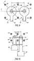
- FIG. 7 is a cross-sectional view taken substantially along line 7 — 7 in FIG. 6 and in FIG. 9 .
- FIG. 8 is a cross-sectional view taken substantially along line 8 — 8 in FIG. 6 and in FIG. 9 .
- FIG. 9 is a top view of two adjacent VCSEL structures showing a non-transparent top contact.
- FIG. 10 is a top view of two adjacent VCSEL structures showing a transparent top contact.
- FIG. 11 shows a laser structure whose aperture is defined by a triangular bounding pattern of cavities.
- FIG. 12 shows an array of lasers which is formed by repeating the triangular bounding pattern shown in FIG. 11 .
- FIG. 13 shows a laser structure whose aperture is defined by a bounding pattern of four cavities arranged in a square pattern.
- FIG. 14 shows an array of lasers which is formed by repeating the square bounding pattern shown in FIG. 13 .
- FIG. 15 shows another array of lasers which is formed by repeating the square bounding pattern shown in FIG. 13 .
- FIG. 16 shows a laser structure whose aperture is defined by a bounding pattern of six cavities arranged in an hexagonal pattern.
- FIG. 17 shows an array of lasers which is formed by repeating the hexagonal bounding pattern shown in FIG. 16 .
- FIG. 18 shows another array of lasers which is formed by an alternative repeating of the hexagonal bounding pattern shown in FIG. 16 .
- FIG. 19 shows a typical planar laterally oxidized VCSEL.
- FIG. 20 shows a light output power versus current plot for a typical planar laterally oxidized VCSEL.
- FIG. 21 shows an embodiment of a planar laterally oxidized VCSEL in accordance with the invention.
- FIG. 22 shows a light output power versus current plot for the embodiment shown in FIG. 21 .
- FIG. 23 shows a misoriented substrate relative to standard crystallographic orientations.
- FIG. 24 shows the orientation of the electric field vector relative to misoriented substrate.
- FIG. 25 shows gain anisotropies for a misoriented substrate.
- FIG. 26 shows an embodiment of a planar laterally oxidized VCSEL in accordance with the invention.
- FIG. 27 shows an embodiment of a planar laterally oxidized VCSEL in accordance with the invention.
- FIG. 3 illustrates a semiconductor structure which is used to form the preferred embodiment of the present invention.
- the structure illustrated includes a number of semiconductor layers, which can be used to form a vertical cavity surface emitting laser. As will be apparent, the layers are illustrated schematically only and bear no relationship to the relative thicknesses each to the other.
- an n-type GaAs buffer layer 102 of approximately 200 nanometers is grown on an n-type GaAs substrate 100 using an epitaxial deposition process known as metal-organic chemical vapor deposition (“MOCVD”).
- MOCVD metal-organic chemical vapor deposition
- the doping level of the n-type GaAs substrate and GaAs buffer are typically around the range of 3 ⁇ 10 18 cm ⁇ 3 to 7 ⁇ 10 18 cm ⁇ 3 so that a reasonably low resistance can be achieved in these layers.
- the semiconductor layers may also be deposited on a substrate by liquid phase epitaxy (“LPE”), molecular beam epitaxy (“MBE”), or other known crystal growth processes.
- the GaAs buffer layer 102 is a superlattice structure for forming a lower distributed Bragg reflector (“DBR”) 104 which provides a portion of the necessary internal reflection in a VCSEL structure.
- the lower DBR 104 is typically formed by multiple pairs of an AlGaAs layer with a high aluminum content (approximately 86% aluminum) and another AlGaAs layer with a low aluminum content (approximately 16% aluminum). After the growth of a number of layer pairs (typically 35 Si doped pseudoparabolically graded DBR pairs), a final AlGaAs layer with a high aluminum content is deposited before growing the first cladding layer 106 of the optical cavity.
- a typical thickness of each layer pair is approximately 120 nanometers for a laser emitting at 820 nanometers.
- the total thickness of each layer pair is designed to be equal to one half of the optical wavelength at the intended wavelength of laser operation.
- the thickness of the final high aluminum content layer is designed to be a quarter of the optical wavelength at the intended wavelength of laser operation.
- the AlGaAs layer with a high aluminum content contains approximately 86% aluminum.
- the aluminum content of the AlGaAs layer with a high aluminum content should be sufficiently high to provide for a low refractive index, but not so high as to oxidize easily.
- the AlGaAs layer with a low aluminum content has an aluminum content of approximately 16%.
- the composition of the AlGaAs layer with a low aluminum content should typically have sufficient aluminum so that it is non-absorptive at the lasing wavelength.
- the reflectivity of the lower DBR 104 should be as close to 100% as possible in order to achieve high internal reflection.
- High internal reflection generally reduces the threshold current of a laser.
- the reflectivity of the lower DBR 104 is generally a function of the difference in the refractive indices between the two AlGaAs layers of the superlattice and the number of layer pairs in the structure. The greater the difference in the refractive indices, the fewer number of pairs are required to obtain a given reflectivity. For example, 30 to 40 pairs of AlGaAs layers may be used to form the lower DBR structure 104 .
- an AlGaAs cladding layer 106 is deposited.
- This lower AlGaAs cladding layer 106 has an aluminum content of about 58% and is n-type with a doping level of 1 ⁇ 10 18 cm ⁇ 3 to 5 ⁇ 10 18 cm ⁇ 3 . Its thickness is approximately 100 nanometers.
- the active layer 108 of the laser structure which comprises four InAlGaAs quantum wells with a thickness of about four to ten nanometers, typically about four nanometers, along with five Al 0.35 Ga 0.65 As barriers with a thickness of about two to eight nanometers, typically about six nanometers.
- pure GaAs or AlGaAs with a low aluminum content may be also used to form the quantum well structures.
- Nothing in this invention prevents the use of a single quantum well or other multiple quantum well (“MQW”) structures to form the active layer 108 .
- MQW multiple quantum well
- an upper AlGaAs cladding layer 110 which is structurally similar to the lower AlGaAs cladding layer 106 except for the polarity of its dopants.
- This upper cladding layer 110 has an aluminum content of about 58% but is p-type with a doping level of 1 ⁇ 10 18 cm ⁇ 3 to 4 ⁇ 10 18 cm ⁇ 3 .
- the thickness of top cladding layer 110 is also about 100 nanometers.
- this oxidation layer 112 is above the upper AlGaAs cladding layer 110 .
- this oxidation layer 112 has an aluminum content of approximately 95% and a thickness of about 70 nanometers.
- this oxidation layer 112 constitutes the first layer of an upper DBR mirror and contains a p-type dopant.
- the remainder of an upper DBR mirror 114 which contains p-type doping is deposited.
- the upper DBR mirror 114 is structurally similar to the lower DBR mirror 104 except for the polarity of its dopants. Additionally, the mirror layer closest to each side of the active region generally has a high aluminum content. In this embodiment, this high aluminum content layer is also the oxidation layer 112 .
- the reflectivity of the upper DBR 114 is typically 98% to 99% because light will be outcoupled through the surface of the semiconductor sample. Typically, 20 to 25 pairs of alternate AlGaAs layers are used to form this upper DBR mirror 114 . Typically, a p-AlGaAs current spreading layer and a final 22 nanometer thick p + GaAs layer are grown above top DBR mirror 114 .
- FIG. 4 is a top view of a portion of a mask which may be applied to the semiconductor structure shown in FIG. 3 under the present invention.
- a uniform layer of silicon nitride will be deposited over the entire semiconductor sample.
- a photoresist layer 118 is deposited over the silicon nitride layer and is formed into the mask shown in FIG. 4 by a photolithographic process which removes photoresist material from four circular areas 120 .
- the circular areas 120 form a pre-determined bounding pattern which will later be used to define the resulting aperture of a laser structure.
- the sample then undergoes an etching process during which cylindrical cavities 126 are formed in the semiconductor structure through the four exposed circular areas 120 .
- the etching is performed by a process such as reactive ion etching which provides for the formation of a deep depression with vertical sidewalls.
- the depth of each cylindrical cavity should extend at least into the oxidation layer 112 , as shown in FIG. 5 .
- the semiconductor sample undergoes an oxidation.
- the sample is typically oxidized with water vapor in a nitrogen environment at elevated temperatures, in excess of 350° C.
- the oxidation layer 112 is exposed to the ambient through each cylindrical cavity, as indicated by arrows A.
- the oxidation layer 112 which comprises of AlGaAs with a high aluminum content, is oxidized radially outwards from each cavity 126 , typically until the oxidized regions 124 surrounding each cavity approach one another and overlap, as can be seen in FIG. 6 .
- a small non-oxidized gap between the oxidized regions may be permissible so long as electrical and optical fields are adequately confined.
- the cross section of each cavity has been described as being cylindrical, any suitable cross section may be used.
- the oxidation rate of AlGaAs increases with the aluminum content in a generally exponential manner at constant temperature.
- the time duration of the oxidation process depends upon the aluminum content in the oxidation layer 112 and the oxidation temperature. A desirable, controllable oxidation duration would be a few tens of minutes. Therefore, the layer that is being oxidized is the AlGaAs which has a high aluminum content of close to 95%. The portion of the AlGaAs layer which remains unoxidized controls the current path through the active layer 108 .
- FIG. 6 is a largely simplified top view of the oxidation layer 112 shown in FIG. 3 assuming that all the layers above it have been removed.
- the shaded region 122 represents the laser aperture in oxidation layer 112 which determines the region of laser emission by active layer 108 . It is formed by the oxidation process of the present invention. During the oxidation process, the oxidation fronts emanate through the oxidation layer from the pattern of four cavities 126 , and the shaded region 122 is formed by the intersection of the boundaries of the oxidized regions 124 . The oxidation fronts emanating from the cylindrical cavities 126 are also generally cylindrical, resulting in overlapping oxidized regions 124 . The center of the overlapping regions 124 remains unoxidized. This unoxidized region forms the shaded area 122 , which is the aperture of the laser structure.
- an ion implantation process which is next described, is used to form isolation region 130 to isolate the laser structure from its neighbor.
- the areas 124 are oxidized and the unoxidized portion 122 forms the aperture which controls the current path through the active layer 108 .
- Current flow through that portion of the active layer 108 which lies below the aperture 122 results in an injected density of p-type and n-type carriers, resulting in optical amplification.
- this optical amplification in combination with feedback from the DBR mirrors, 104 and 114 , will result in laser oscillation and emission from the active layer within the region defined by aperture 122 in oxidation layer 112 .
- Isolation region 130 (illustrated in FIGS. 6 , 7 and 8 ), which is formed by using an ion implantation isolation process, is highly resistive.
- the typical implantation energies used in such a process are 50 KeV, 100 KeV, 200 KeV and 310 KeV.
- the dose is typically 3 ⁇ 10 15 cm ⁇ 2 at each energy level.
- the ion used to form the isolation region 402 is typically hydrogen.
- metal contacts 132 and 134 are formed on the top surface and the bottom surface of the semiconductor structure, respectively, for biasing the laser, as illustrated in FIGS. 7 , 8 and 9 .
- a typical material used for forming the contacts is a titanium/gold bilayer film.
- FIG. 9 shows a top view of a VCSEL structure formed in accordance to the present invention after a typical metallization process to form the top contact 132 . Views in the direction of section lines 7 — 7 and 8 — 8 in this Figure are also as illustrated in FIGS. 7 and 8 .
- the top contact 132 is of a generally keyhole shape, including a circular portion 134 and an extension portion 136 .
- the circular portion lies inboard of the cavities 126 and overlies the laser aperture 122 . Since it is non-transparent it is made annular in shape so as to allow light to be coupled out of the laser through its central opening.
- the width “W” of the annular circular portion 134 is usually limited by the minimum line width achievable under the processing technology used, thus setting a lower limit on the pitch between adjacent VCSEL structures Thus, a typical pitch between the centers of two adjacent VCSEL apertures 122 would be “4W.” However, if a transparent conductor is used (e.g. see FIG. 10 ), the pitch between adjacent VCSEL structures could be further reduced to be on the order of “2W” because the top contact could overlie the laser aperture 122 . Moreover, the contact arrangement provides a direct current path to the optical mode at the center of aperture 122 and may be useful in applications where reduced mode partition noise is desired.
- ITO indium tin oxide
- This procedure is self-aligned and greatly simplifies fabrication and is enabled by the stability of ITO during the lateral oxidation process (see “Low-threshold InAlGaAs vertical-cavity surface-emitting laser arrays using transparent electrodes” by C. L. Chua et al. in Applied Physics Letters, vol. 72, no. 9, 1001, which is incorporated by reference in its entirety).
- a half-wavelength thick ITO film is first deposited over the p + GaAs contact layer overlying p-AlGaAs current spreading layer which is grown over DBR layer 114 .
- the ITO film is then successively rapid thermal annealed at 300 and at 600° C. for 2 min each in a nitrogen ambient.
- the low-temperature anneal crystallizes the deposited amorphous ITO film, while the second, higher-temperature anneal induces ohmic contact formation between the ITO film and the p + GaAs contact layer.
- the transparent ITO film attains a post anneal contact resistance of 2 ⁇ 10 ⁇ 5 ohm cm 2 , a sheet resistivity of 5 ⁇ 10 ⁇ 4 ohm cm, and a power transmission coefficient of 98% at an emission wavelength of 817 nanometers.
- a set of cavities 126 typically having a diameter of 2 ⁇ m delineating laser aperture 122 is patterned as shown in FIG. 10 for example.
- the ITO and underlying DBR layers 114 are then dry etched using chemically assisted ion beam etching in two successive self-aligned steps to form cavities 126 that reach oxidation layer 112 , typically Al 0.94 Ga 0.06 As.
- Oxidation layer 112 is oxidized for 45 minutes at 415° C. in flowing steam.
- Oxidized regions 124 progress laterally outwards from each cavity 126 , and on merging define laser aperture 122 .
- Apertures 122 may typically range from 5 ⁇ m to 43 ⁇ m in diameter.
- Positioning of cavities 126 is typically selected so that lateral oxidation needs to proceed by only a few micrometers from the perimeters of cavities 126 .
- This reduced path of oxidation compared to typical etched pillar devices reduces the sensitivity of laser aperture 126 to variations in oxidation rates.
- the aluminum content of oxidation layer 112 is relatively low in order to lengthen the oxidation time so that transients are minimized.
- the ITO film is not effected by the oxidation process.
- top contact is shown in FIG. 10 and is identified by numeral 138 . It comprises a transparent conductive contact finger 140 and contact pad 142 , the contact finger overlying the laser aperture 122 .
- the bottom electrode 134 is formed by depositing metal on the bottom surface of the substrate 100 and is typically an evaporated eutectic Ge/Au metal.
- FIGS. 11 , and 12 , 13 , 14 and 15 , and 16 , 17 and 18 illustrate alternative packing arrangements for forming an array of lasers formed by the method of the present invention.
- each laser structure includes an aperture 222 defined by oxidized regions 224 surrounding a bounding pattern of three cylindrical cavities 226 positioned at the apexes of an equilateral triangle.
- the spacing between the centers of any two cavities is “S.”
- an embedded AlGaAs layer with a high aluminum content will be oxidized radially outwardly from the cylindrical cavities 226 until the oxidized regions 224 overlap to form the unoxidized laser aperture 222 .
- the packing arrangement shown in FIG. 11 may be repeated to form a laser array as shown in FIG. 12 . If the spacing between the centers of two cylindrical cavities is “S,” a typical linear spacing “L” between two laser apertures is approximately “S/2.”
- FIG. 13 In the laser device of FIG. 13 and the arrays of FIGS. 14 and 15 , the square bounding pattern of cylindrical cavities 126 is illustrated. Oxidized regions 124 will overlap to form the unoxidized laser aperture 122 .
- This packing arrangement shown in FIG. 13 may be repeated to form a laser array as shown in FIG. 14 or 15 If a packing arrangement such as FIG. 14 is used and the spacing between the centers of two adjacent cylindrical cavities is “S,” a typical linear spacing “L” between two laser apertures is approximately “S.” If an arrangement such as FIG. 15 is used and the spacing between the centers of two cylindrical depressions is “S,” a typical linear spacing “L” between two laser apertures is approximately “ ⁇ 2 ⁇ S.”
- the cavities 326 may also be arranged at the vertices of any other polygon.
- the laser aperture is formed by the unoxidized region 322 defined by the oxidized regions 324 .
- the packing arrangement shown in FIG. 16 may be repeated to form a laser array as shown in FIG. 17 or 18 . If an arrangement such as FIG. 17 is used and the spacing between the centers of two adjacent cylindrical cavities is “S,” a typical linear spacing “L” between two laser apertures is approximately “1.5S.” If an arrangement such as FIG. 18 is used, the closest linear spacing “L” between two laser apertures is approximately “ ⁇ 3 ⁇ 0.5S.”
- composition, dopants, doping levels, and dimensions given above are exemplary only, and variations in these parameters are permissible. Additionally, other layers in addition to the ones shown in the figures may also be included. Variations in experimental conditions such as temperature and time are also permitted. Lastly, instead of GaAs and GaAlAs, other semiconductor materials such as GaAlSb, InAlGaP, or other III-V alloys may also be used.
- the planar laterally-oxidized (PLO) VCSELs described above utilize holes or cavities 126 , 226 or 326 to penetrate upper DBR mirror 114 .
- Cavities 126 , 226 or 326 serve to expose buried high aluminum layer 112 that is then selectively oxidized.
- Cavities 126 , 226 or 326 may be arranged at the vertices of a polygon such that upon oxidation, the oxidized regions, such as oxidized regions 124 of cavities 126 border VCSEL aperture 122 .
- oxidized regions 124 bordering aperture 122 have a refractive index lower than the refractive index of aperture 122 and are electrically insulating, oxidized regions 124 form a good lateral waveguide that also functions to confine current to aperture 122 .
- the planar surface areas between cavities 126 allows electrical contacting and routing to be established in a planar manner. Inter-device isolation is accomplished using ion implantation.
- FIG. 19 shows planar laterally oxidized (PLO) VCSEL 400 .
- cavities 426 have a 2 ⁇ m diameter and cavities 426 are placed at the vertices of a regular octagon. Cavities 426 are typically positioned with a center to center spacing of about 5 ⁇ m. Oxidation regions 424 extend by about 3.5 ⁇ m from the edges of cavities 126 , typically leaving aperture 422 with a 4 ⁇ m width. Light is emitted from aperture 422 of VCSEL 400 through ITO electrode 438 .
- FIG. 20 shows the light output power versus current characteristics of an embodiment of VCSEL 400 .
- Curve 2071 shows the light from VCSEL 400 with no polarization filter applied.
- Curve 2072 shows the light from VCSEL 400 having a polarization along direction 2320 (see FIG. 23 ) inclined at an angle of about 4.1 degrees relative to the [011] crystallographic direction.
- Curve 2073 shows light from VCSEL 400 having a polarization along the [011] crystallographic direction.
- FIG. 20 shows that the light from VCSEL 400 is initially polarized along direction 2325 which is the [011] direction but that the polarization switches abruptly to direction 2320 (see FIG.
- Embodiments of VCSEL 400 that are seemingly identical may behave differently with respect to the polarization direction and polarization switching as shown in “Anisotropic apertures for polarization-stable laterally oxidized vertical-cavity lasers” by Chua et al., Applied Physics Letters vol. 73, no. 12, pp. 1631–1633 which is incorporated by reference in its entirety. This is indicative of the polarization instability inherent in conventional devices such as, for example, VCSEL 400 .
- FIG. 21 shows this symmetry breaking may be created by making aperture 522 asymmetric by arranging holes or cavities 426 at the vertices of a distorted octagon.
- the distorted octagon is compressed by, for example, about 1.5 ⁇ m along the [011] direction and elongated by 1.5 ⁇ m along direction 2320 (see FIG. 23 ).
- oval-like aperture 522 is formed. Ion implantation is performed outside of ellipsoidal region 531 consistent with the discussion above.
- AlGaAs layer 124 surrounding aperture 122 contracts and the change in thickness of layer 124 results in mechanical stresses at the boundary between layer 124 and aperture 122 (see FIG. 7 ).
- the anisotropic stress resulting from oval-like aperture 522 removes the polarization modal gain degeneracy.
- a significant polarization preference is established along one of the two orthogonal axes resulting in stable polarization independent of the current level in the operating range.
- the difference in gain available to the two orthogonal polarization states is due to the differential gain that develops with the asymmetric stress and the different modal gain resulting from stress-induced birefringence.
- FIG. 22 shows polarization-resolved light output power versus current curves obtained from an embodiment of VCSEL 500 in accordance with the present invention.
- Curve 2271 shows the light output power without polarization filter.
- Curve 2272 shows that laser output in direction 2320 (see FIG. 23 ) is completely suppressed throughout the operating regime.
- Curve 2273 shows that VCSEL 500 displays stable polarization along the [011] direction throughout the operating regime.
- the polarization suppression ratio is 18 dB for curve 2272 relative to curve 2273 at a current level of about 2.5 mA where peak light output power is reached.
- Substrate 2300 used in one embodiment of VCSEL 500 in accordance with the present invention has the characteristics as shown in FIG. 22 with a substrate surface cut in a crystal plane that is tilted toward the [011] crystallographic axis.
- FIG. 23 shows misoriented substrate 2300 with surface vector 2310 misoriented relative to [100] direction 2305 of a (100) oriented substrate surface. The misorientation is by angle of rotation ⁇ about [011] direction 2325 toward [011] direction 2315 . Misorientation relative to any of the ⁇ 111> axes also results in anisotropic polarization selectivity.
- angle of rotation ⁇ is about 4.1 degrees.
- Groups of VCSEL 500 may be made in arrays resulting, for example, in arrays similar to those shown in FIGS. 17 and 18 with printer and other applications.
- FIG. 24 shows the orientation of electric field vector E at polarization angle ⁇ ′ with respect to axis 2320 of an embodiment of misoriented substrate 2300 in accordance with this invention for light exiting substrate 2300 .
- FIG. 25 shows the corresponding gain that is achieved in arbitrary units versus the polarization angle ⁇ ′ for an embodiment of misoriented substrate 2300 .
- the gain is seen to vary with polarization angle ⁇ ′ in a periodic manner.
- the gain is higher for E fields polarized along ⁇ [011] direction 2325 . Therefore, misoriented substrate 2300 favors laser light polarized in ⁇ [011] direction 2325 over laser light polarized in ⁇ direction 2320 .
- substrates that are misoriented along a different direction and by different angles can also produce gain anisotropies.
- standard (100)-oriented substrates have crystal symmetries that belong to the D 4th point group, their gain properties are isotropic in the substrate plane as a function of angle.
- Misoriented substrates can have symmetries that produce gain anisotropies leading to directional gain dependencies as shown, for example, in FIG. 25 for an embodiment of substrate 2300 .
- Gain curves for a given substrate orientation can be determined by first calculating the quantum wave functions using the multiband effective mass theory for the valence band and Kane's model (e.g., see E. O. Kane, in Journal of Physics and Chemistry of Solids, v. 1, p. 249, (1957), incorporated by reference in its entirety) for the conduction band.
- the valence band Hamiltonian for a (100) substrate consists of the Luttinger-Kohn Hamiltonian (e.g., see J. M. Luttinger and W. Kohn in Physical Review, v. 97, p. 869 (1955), incorporated by reference in its entirety) and a strain-orbit potential term if the active layer is under stress. Details regarding the strain-orbital term may be found in G. E. Pikus and G. L. Bir in Soviet Physics-Solid State, vol. 1, 1502 (1960) incorporated by reference in its entirety.
- stress on active layer 108 occurs because of the lattice mismatch between active layer 108 and GaAs substrate 100 resulting in a stress ranging from 0.01% to 1%, and typically about 0.5% compressive stress for the embodiment shown in FIGS. 21 and 22 .
- the amount and type of built-in active layer stress depends on the particular alloy chosen for the quantum wells in active layer 108 . Possible alloys for quantum wells include InAlGaAs, AlGaInP, InGaAsN and AlGaAsSb.
- cavities may be used to induce stress.
- the energy band structure may be solved for numerically.
- the gain curve as a function of direction is then obtained by calculating the density of states and evaluating the relevant optical matrix elements.
- the substrate orientation necessary to produce a desired gain versus polarization angle dependency can be investigated, for example, by using the PICS3D software program available from Crosslight Software, Inc. at 5450 Canotek Road, Unit 56, Gloucester, Ontario, Canada K1J9G4.
- FIG. 26 shows VCSEL 400 with etched cavities 2601 and 2602 in accordance with an embodiment of this invention.
- Aperture 422 is not asymmetric but cavities 2601 and 2602 are etched on either side of VCSEL 400 , typically placed as close as possible to aperture 422 , to induce an asymmetry on active region of VCSEL 400 .
- One cavity or more than two cavities may also be used to generate differential loss and/or stress on VCSEL 400 .
- cavities 2601 and 2602 are etched at the same time and using the same process as cavities 426 .
- the depth of cavities 2601 and 2602 is about the same as the depth of cavities 426 .
- cavities 2601 and 2602 can also be formed at a different time and using a different process from cavities 426 .
- cavities 2601 and 2602 in an embodiment in accordance with the invention may be formed using focused ion beam milling subsequent to fabrication of VCSEL 400 .
- Cavities 2601 and 2602 may be filled with a filler material having a coefficient of thermal expansion different from substrate 100 to enhance the function of cavities 2601 and 2602 (see FIG. 3 ).
- cavities 2601 and 2602 may be filled with a metal, semiconductor or dielectric material. The filler material is deposited at temperatures well in excess of the operating temperature of VCSEL 400 so that as the filler cools a stress is induced in VCSEL 400 .
- cavities 2601 and 2602 may be oriented perpendicular to the direction of polarization reinforced by misoriented substrate 2300 to further suppress the polarization instability for VCSEL 400 .
- FIG. 27 shows VCSEL 500 with etched cavities 2701 and 2702 in accordance with an embodiment of this invention.
- Aperture 522 is asymmetric and cavities 2701 and 2702 are etched on either side of VCSEL 500 , typically placed as close as possible to aperture 522 , to reinforce the asymmetry on the active region of VCSEL 500 .
- One cavity or more than two cavities may also be used to generate differential loss and/or stress on VCSEL 500 .
- cavities 2701 and 2702 are etched at the same time and using the same process as cavities 426 .
- the depth of cavities 2701 and 2702 is about the same as the depth of cavities 426 .
- cavities 2701 and 2702 can also be formed at a different time and using a different process from cavities 426 .
- cavities 2701 and 2702 in accordance with an embodiment the invention may be formed using focused ion beam milling subsequent to fabrication of VCSEL 500 .
- Cavities 2701 and 2702 may be filled with a filler material having a coefficient of thermal expansion different from substrate 100 to enhance the function of cavities 2701 and 2702 (see FIG. 3 ).
- cavities 2701 and 2702 may be filled with a metal, semiconductor or dielectric material. The filler material is deposited at temperatures well in excess of the operating temperature of VCSEL 500 so that as the filler cools a stress is induced in VCSEL 500 .
- cavities 2701 and 2702 and the major axis of aperture 522 may be oriented perpendicular to the direction of polarization reinforced by misoriented substrate 2300 to further suppress the polarization instability for VCSEL 500 .
Landscapes
- Physics & Mathematics (AREA)
- Optics & Photonics (AREA)
- Condensed Matter Physics & Semiconductors (AREA)
- General Physics & Mathematics (AREA)
- Electromagnetism (AREA)
- Chemical & Material Sciences (AREA)
- Engineering & Computer Science (AREA)
- Nanotechnology (AREA)
- Life Sciences & Earth Sciences (AREA)
- Biophysics (AREA)
- Crystallography & Structural Chemistry (AREA)
- Semiconductor Lasers (AREA)
Abstract
Description
Claims (15)
Priority Applications (2)
| Application Number | Priority Date | Filing Date | Title |
|---|---|---|---|
| US09/933,960 US7160749B2 (en) | 1997-02-07 | 2001-08-20 | Method and structure for eliminating polarization instability in laterally—oxidized VCSELs |
| US11/404,800 US7596161B2 (en) | 1997-02-07 | 2006-04-17 | Laterally oxidized vertical cavity surface emitting lasers |
Applications Claiming Priority (5)
| Application Number | Priority Date | Filing Date | Title |
|---|---|---|---|
| US3717597P | 1997-02-07 | 1997-02-07 | |
| US08/940,867 US5978408A (en) | 1997-02-07 | 1997-09-30 | Highly compact vertical cavity surface emitting lasers |
| US36461499A | 1999-07-29 | 1999-07-29 | |
| US09/389,160 US6304588B1 (en) | 1997-02-07 | 1999-09-02 | Method and structure for eliminating polarization instability in laterally-oxidized VCSELs |
| US09/933,960 US7160749B2 (en) | 1997-02-07 | 2001-08-20 | Method and structure for eliminating polarization instability in laterally—oxidized VCSELs |
Related Parent Applications (1)
| Application Number | Title | Priority Date | Filing Date |
|---|---|---|---|
| US09/389,160 Division US6304588B1 (en) | 1997-02-07 | 1999-09-02 | Method and structure for eliminating polarization instability in laterally-oxidized VCSELs |
Related Child Applications (1)
| Application Number | Title | Priority Date | Filing Date |
|---|---|---|---|
| US11/404,800 Division US7596161B2 (en) | 1997-02-07 | 2006-04-17 | Laterally oxidized vertical cavity surface emitting lasers |
Publications (2)
| Publication Number | Publication Date |
|---|---|
| US20050158902A1 US20050158902A1 (en) | 2005-07-21 |
| US7160749B2 true US7160749B2 (en) | 2007-01-09 |
Family
ID=34753838
Family Applications (3)
| Application Number | Title | Priority Date | Filing Date |
|---|---|---|---|
| US09/389,160 Expired - Lifetime US6304588B1 (en) | 1997-02-07 | 1999-09-02 | Method and structure for eliminating polarization instability in laterally-oxidized VCSELs |
| US09/933,960 Expired - Lifetime US7160749B2 (en) | 1997-02-07 | 2001-08-20 | Method and structure for eliminating polarization instability in laterally—oxidized VCSELs |
| US11/404,800 Expired - Fee Related US7596161B2 (en) | 1997-02-07 | 2006-04-17 | Laterally oxidized vertical cavity surface emitting lasers |
Family Applications Before (1)
| Application Number | Title | Priority Date | Filing Date |
|---|---|---|---|
| US09/389,160 Expired - Lifetime US6304588B1 (en) | 1997-02-07 | 1999-09-02 | Method and structure for eliminating polarization instability in laterally-oxidized VCSELs |
Family Applications After (1)
| Application Number | Title | Priority Date | Filing Date |
|---|---|---|---|
| US11/404,800 Expired - Fee Related US7596161B2 (en) | 1997-02-07 | 2006-04-17 | Laterally oxidized vertical cavity surface emitting lasers |
Country Status (1)
| Country | Link |
|---|---|
| US (3) | US6304588B1 (en) |
Cited By (6)
| Publication number | Priority date | Publication date | Assignee | Title |
|---|---|---|---|---|
| US20100166032A1 (en) * | 2007-12-17 | 2010-07-01 | Palo Alto Research Center Incorporated | Buried Aperture Nitride Light-Emiting Device |
| US9553423B2 (en) | 2015-02-27 | 2017-01-24 | Princeton Optronics Inc. | Miniature structured light illuminator |
| US10305254B2 (en) | 2017-09-18 | 2019-05-28 | Finisar Corporation | VCSEL with elliptical aperture having reduced rin |
| US10985531B2 (en) | 2019-01-27 | 2021-04-20 | Hewlett Packard Enterprise Development Lp | Intensity noise mitigation for vertical-cavity surface emitting lasers |
| US11289881B2 (en) | 2019-05-08 | 2022-03-29 | Ii-Vi Delaware, Inc. | Oxide aperture shaping in vertical cavity surface-emitting laser |
| US20240348016A1 (en) * | 2023-04-11 | 2024-10-17 | Lumentum Operations Llc | Vertical-cavity surface-emitting laser with asymmetric aperture for improved polarization stability |
Families Citing this family (43)
| Publication number | Priority date | Publication date | Assignee | Title |
|---|---|---|---|---|
| US6304588B1 (en) * | 1997-02-07 | 2001-10-16 | Xerox Corporation | Method and structure for eliminating polarization instability in laterally-oxidized VCSELs |
| US6577658B1 (en) * | 1999-09-20 | 2003-06-10 | E20 Corporation, Inc. | Method and apparatus for planar index guided vertical cavity surface emitting lasers |
| JP4010095B2 (en) * | 1999-10-01 | 2007-11-21 | 富士ゼロックス株式会社 | Surface emitting semiconductor laser and laser array |
| US6928415B1 (en) | 2000-06-05 | 2005-08-09 | Barnet L. Liberman | Method of delivering groceries purchased over the internet |
| US6810064B1 (en) * | 2000-08-22 | 2004-10-26 | The Regents Of The University Of California | Heat spreading layers for vertical cavity surface emitting lasers |
| EP1225669B1 (en) * | 2001-01-17 | 2004-07-28 | Avalon Photonics Ltd. | A polarization-stable vertical cavity surface emitting laser device and a method of stabilizing the polarization of such a laser device |
| DK1371120T3 (en) * | 2001-03-09 | 2013-07-22 | Alight Photonics Aps | WAVE TYPE CONTROL USING TRANSVERSAL TAPE STRUCTURE IN VCSELS |
| JP4621393B2 (en) * | 2001-03-27 | 2011-01-26 | 富士ゼロックス株式会社 | Surface emitting semiconductor laser and method for manufacturing surface emitting semiconductor laser |
| US6813295B2 (en) * | 2002-03-25 | 2004-11-02 | Agilent Technologies, Inc. | Asymmetric InGaAsN vertical cavity surface emitting lasers |
| US6872983B2 (en) * | 2002-11-11 | 2005-03-29 | Finisar Corporation | High speed optical transceiver package using heterogeneous integration |
| US7257141B2 (en) * | 2003-07-23 | 2007-08-14 | Palo Alto Research Center Incorporated | Phase array oxide-confined VCSELs |
| JP2007504639A (en) * | 2003-08-29 | 2007-03-01 | オスラム オプト セミコンダクターズ ゲゼルシャフト ミット ベシュレンクテル ハフツング | Radiation emission semiconductor device |
| US7122398B1 (en) * | 2004-03-25 | 2006-10-17 | Nanosolar, Inc. | Manufacturing of optoelectronic devices |
| US20050224701A1 (en) * | 2004-03-30 | 2005-10-13 | Xerox Corporation | Light-based data communication in a data-processing system |
| TWI322461B (en) * | 2004-08-30 | 2010-03-21 | Prime View Int Co Ltd | Method of fabricating poly-crystal ito thin film and poly-crystal ito electrode |
| US8000374B2 (en) * | 2005-04-20 | 2011-08-16 | Finisar Corporation | Surface gratings on VCSELs for polarization pinning |
| US20070098032A1 (en) * | 2005-10-27 | 2007-05-03 | Finisar Corporation | Polarization control in vertical cavity surface emitting lasers using off-axis epitaxy |
| WO2007116659A1 (en) * | 2006-03-23 | 2007-10-18 | Nec Corporation | Surface light-emitting laser |
| DE102006057747B4 (en) * | 2006-09-27 | 2015-10-15 | Osram Opto Semiconductors Gmbh | Semiconductor body and semiconductor chip with a semiconductor body |
| JP2008153341A (en) * | 2006-12-15 | 2008-07-03 | Rohm Co Ltd | Surface emitting laser |
| JP2008177430A (en) * | 2007-01-19 | 2008-07-31 | Sony Corp | LIGHT EMITTING ELEMENT AND ITS MANUFACTURING METHOD, AND LIGHT EMITTING ELEMENT ASSEMBLY AND ITS MANUFACTURING METHOD |
| JP5177130B2 (en) * | 2007-03-23 | 2013-04-03 | 住友電気工業株式会社 | Photonic crystal laser and photonic crystal laser manufacturing method |
| JP4350774B2 (en) * | 2007-07-31 | 2009-10-21 | キヤノン株式会社 | Surface emitting laser |
| JP4347369B2 (en) | 2007-07-31 | 2009-10-21 | キヤノン株式会社 | Manufacturing method of surface emitting laser |
| JP2009295792A (en) | 2008-06-05 | 2009-12-17 | Ricoh Co Ltd | Surface-emitting laser element, surface-emitting laser array, optical scanning device, and image forming apparatus |
| GB0817786D0 (en) * | 2008-09-30 | 2008-11-05 | Bookham Technology Plc | Improved vertical cavity surface emitting laser |
| KR101735670B1 (en) * | 2010-07-13 | 2017-05-15 | 엘지이노텍 주식회사 | A light emitting device |
| US8537874B2 (en) * | 2010-10-28 | 2013-09-17 | Flir Systems, Inc. | High fill-factor efficient vertical-cavity surface emitting laser arrays |
| US9088134B2 (en) * | 2011-07-27 | 2015-07-21 | Vixar Inc. | Method and apparatus including improved vertical-cavity surface-emitting lasers |
| US20130069242A1 (en) * | 2011-09-20 | 2013-03-21 | Taiwan Semiconductor Manufacturing Co., Ltd. | Arrangement of through-substrate vias for stress relief and improved density |
| EP2865056B1 (en) * | 2012-06-26 | 2025-08-06 | TRUMPF Photonic Components GmbH | Laser module for homogeneous line-shaped intensity profiles |
| US10530129B2 (en) * | 2015-08-10 | 2020-01-07 | Hewlett Packard Enterprise Development Lp | Low impedance VCSELs |
| US9742153B1 (en) * | 2016-02-23 | 2017-08-22 | Lumentum Operations Llc | Compact emitter design for a vertical-cavity surface-emitting laser |
| US10355456B2 (en) | 2017-09-26 | 2019-07-16 | Lumentum Operations Llc | Emitter array with variable spacing between adjacent emitters |
| KR102425083B1 (en) * | 2017-10-19 | 2022-07-27 | 쑤저우 레킨 세미컨덕터 컴퍼니 리미티드 | Semiconductor device, semiconductor device package and automatic forcusing apparatus |
| US11984703B2 (en) | 2018-05-10 | 2024-05-14 | Suzhou Lekin Semiconductor Co., Ltd. | Surface emitting laser device and a light emitting device including the same |
| CN108598866B (en) * | 2018-05-21 | 2020-02-14 | 湖北光安伦科技有限公司 | VCSEL chip array structure and manufacturing method thereof |
| KR20200025005A (en) * | 2018-08-29 | 2020-03-10 | 엘지이노텍 주식회사 | A surface-emitting laser device and light emitting device including the same |
| CN110416874B (en) * | 2019-09-18 | 2020-01-17 | 常州纵慧芯光半导体科技有限公司 | Method for preparing small-spacing vertical cavity surface emitting laser array |
| US12308618B2 (en) * | 2021-04-26 | 2025-05-20 | Lumentum Operations Llc | Matrix addressable vertical cavity surface emitting laser array |
| US12334711B2 (en) * | 2021-05-19 | 2025-06-17 | Mellanox Technologies, Ltd. | Fabricating semiconductor devices, such as VCSELs, with an oxide confinement layer |
| US20240186766A1 (en) * | 2022-10-19 | 2024-06-06 | Ii-Vi Delaware, Inc. | Polarized/lensed back-side emitting (bse) vertical-cavity surface-emitting laser (vcsel) |
| CN118054297A (en) * | 2024-02-06 | 2024-05-17 | 浙江博升光电科技有限公司 | A test structure for vertical cavity surface emitting laser and a manufacturing method thereof |
Citations (56)
| Publication number | Priority date | Publication date | Assignee | Title |
|---|---|---|---|---|
| US4144101A (en) | 1978-06-05 | 1979-03-13 | International Business Machines Corporation | Process for providing self-aligned doping regions by ion-implantation and lift-off |
| US4216036A (en) | 1978-08-28 | 1980-08-05 | Bell Telephone Laboratories, Incorporated | Self-terminating thermal oxidation of Al-containing group III-V compound layers |
| US4233387A (en) | 1979-03-05 | 1980-11-11 | Xerox Corporation | Electrophotographic carrier powder coated by resin dry-mixing process |
| US4810611A (en) | 1987-11-02 | 1989-03-07 | Xerox Corporation | Developer compositions with coated carrier particles having incorporated therein colorless additives |
| US5073041A (en) | 1990-11-13 | 1991-12-17 | Bell Communications Research, Inc. | Integrated assembly comprising vertical cavity surface-emitting laser array with Fresnel microlenses |
| US5115442A (en) | 1990-04-13 | 1992-05-19 | At&T Bell Laboratories | Top-emitting surface emitting laser structures |
| US5115441A (en) | 1991-01-03 | 1992-05-19 | At&T Bell Laboratories | Vertical cavity surface emmitting lasers with transparent electrodes |
| US5126875A (en) | 1989-07-19 | 1992-06-30 | Fujitsu Limited | Semiconductor optical device having a variable refractive index profile |
| US5171703A (en) | 1991-08-23 | 1992-12-15 | Intel Corporation | Device and substrate orientation for defect reduction and transistor length and width increase |
| US5179567A (en) | 1990-03-06 | 1993-01-12 | Hitachi, Ltd. | Semiconductor laser device, method of fabricating the same and optical system of utilizing the same |
| US5245622A (en) | 1992-05-07 | 1993-09-14 | Bandgap Technology Corporation | Vertical-cavity surface-emitting lasers with intra-cavity structures |
| US5258990A (en) | 1991-11-07 | 1993-11-02 | The United States Of America As Represented By The Secretary Of The United States Department Of Energy | Visible light surface emitting semiconductor laser |
| US5262360A (en) | 1990-12-31 | 1993-11-16 | The Board Of Trustees Of The University Of Illinois | AlGaAs native oxide |
| US5262491A (en) | 1991-03-29 | 1993-11-16 | General Electric Company | High performance curable PPO/monomeric epoxy compositions with tin metal salt compatibilizing agent |
| US5327448A (en) | 1992-03-30 | 1994-07-05 | The Board Of Trustees Of The University Of Illinois | Semiconductor devices and techniques for controlled optical confinement |
| US5331654A (en) | 1993-03-05 | 1994-07-19 | Photonics Research Incorporated | Polarized surface-emitting laser |
| US5337074A (en) | 1990-12-28 | 1994-08-09 | Xerox Corporation | Opto-electronic line printer having a high density, independently addressable, surface emitting semiconductor laser/light emitting diode array |
| US5354709A (en) | 1986-11-10 | 1994-10-11 | The United States Of America As Represented By The Secretary Of The Air Force | Method of making a lattice mismatched heterostructure optical waveguide |
| US5359618A (en) | 1993-06-01 | 1994-10-25 | Motorola, Inc. | High efficiency VCSEL and method of fabrication |
| US5400354A (en) | 1994-02-08 | 1995-03-21 | Ludowise; Michael | Laminated upper cladding structure for a light-emitting device |
| US5412680A (en) * | 1994-03-18 | 1995-05-02 | Photonics Research Incorporated | Linear polarization of semiconductor laser |
| US5416044A (en) | 1993-03-12 | 1995-05-16 | Matsushita Electric Industrial Co., Ltd. | Method for producing a surface-emitting laser |
| US5493577A (en) | 1994-12-21 | 1996-02-20 | Sandia Corporation | Efficient semiconductor light-emitting device and method |
| US5550081A (en) | 1994-04-08 | 1996-08-27 | Board Of Trustees Of The University Of Illinois | Method of fabricating a semiconductor device by oxidizing aluminum-bearing 1H-V semiconductor in water vapor environment |
| US5557627A (en) | 1995-05-19 | 1996-09-17 | Sandia Corporation | Visible-wavelength semiconductor lasers and arrays |
| US5568499A (en) | 1995-04-07 | 1996-10-22 | Sandia Corporation | Optical device with low electrical and thermal resistance bragg reflectors |
| US5594751A (en) | 1995-06-26 | 1997-01-14 | Optical Concepts, Inc. | Current-apertured vertical cavity laser |
| EP0772269A1 (en) | 1995-10-31 | 1997-05-07 | Hewlett-Packard Company | Vertical-cavity surface-emitting laser |
| US5633527A (en) | 1995-02-06 | 1997-05-27 | Sandia Corporation | Unitary lens semiconductor device |
| US5659193A (en) | 1993-12-10 | 1997-08-19 | Mitsubishi Denki Kabushiki Kaisha | Semiconductor device and method for manufacturing the same |
| JPH09223841A (en) | 1996-02-16 | 1997-08-26 | Nippon Telegr & Teleph Corp <Ntt> | Surface emitting laser and manufacturing method thereof |
| US5717533A (en) | 1995-01-13 | 1998-02-10 | Methode Electronics Inc. | Removable optoelectronic module |
| US5719892A (en) | 1996-04-23 | 1998-02-17 | Motorola, Inc. | Hybrid mirror structure for a visible emitting VCSEL |
| US5719891A (en) | 1995-12-18 | 1998-02-17 | Picolight Incorporated | Conductive element with lateral oxidation barrier |
| US5724374A (en) | 1996-08-19 | 1998-03-03 | Picolight Incorporated | Aperture comprising an oxidized region and a semiconductor material |
| JPH1065266A (en) | 1996-08-21 | 1998-03-06 | Fuji Xerox Co Ltd | Planar emitting type semiconductor laser element, planar emitting type semiconductor laser array, planar emitting type semiconductor laser beam scanner, planar emitting laser beam recording device and laser recording method |
| US5729566A (en) | 1996-06-07 | 1998-03-17 | Picolight Incorporated | Light emitting device having an electrical contact through a layer containing oxidized material |
| US5734588A (en) | 1995-01-17 | 1998-03-31 | Electric Power Research Institute Inc. | Bore probe for tube inspection with guided waves and method therefor |
| US5739945A (en) | 1995-09-29 | 1998-04-14 | Tayebati; Parviz | Electrically tunable optical filter utilizing a deformable multi-layer mirror |
| JPH10125999A (en) | 1996-09-02 | 1998-05-15 | Matsushita Electric Ind Co Ltd | Surface emitting semiconductor laser and method of manufacturing the same |
| US5778018A (en) * | 1994-10-13 | 1998-07-07 | Nec Corporation | VCSELs (vertical-cavity surface emitting lasers) and VCSEL-based devices |
| EP0858137A2 (en) | 1997-02-07 | 1998-08-12 | Xerox Corporation | Surface emitting laser devices and method of manufacture |
| US5809051A (en) | 1995-09-22 | 1998-09-15 | France Telecom | Vertical cavity laser emission component that emits via the surface at a wavelength lying in the range 1.3 micrometers to 1.55 micrometers and a method for making it |
| US5864468A (en) | 1995-01-13 | 1999-01-26 | Methode Electronics, Inc. | Removable optoelectronic module with grounding means |
| EP0898344A2 (en) | 1997-08-15 | 1999-02-24 | Hewlett-Packard Company | Near planar native-oxid VCSEL device and arrays |
| US5881085A (en) | 1996-07-25 | 1999-03-09 | Picolight, Incorporated | Lens comprising at least one oxidized layer and method for forming same |
| US5903588A (en) | 1997-03-06 | 1999-05-11 | Honeywell Inc. | Laser with a selectively changed current confining layer |
| US6052399A (en) | 1997-08-29 | 2000-04-18 | Xerox Corporation | Independently addressable laser array with native oxide for optical confinement and electrical isolation |
| US6069908A (en) | 1998-02-09 | 2000-05-30 | Hewlwtt-Packard Company | N-drive or P-drive VCSEL array |
| US6075804A (en) | 1998-01-28 | 2000-06-13 | Picolight Incorporated | Semiconductor device having an oxide defined aperture |
| US6148016A (en) | 1997-11-06 | 2000-11-14 | The Regents Of The University Of California | Integrated semiconductor lasers and photodetectors |
| US6188711B1 (en) * | 1997-12-18 | 2001-02-13 | Agilent Technologies, Inc. | Polarization-controlled VCSELs using externally applied uniaxial stress |
| US6304588B1 (en) * | 1997-02-07 | 2001-10-16 | Xerox Corporation | Method and structure for eliminating polarization instability in laterally-oxidized VCSELs |
| US6459719B1 (en) | 1997-12-12 | 2002-10-01 | Honeywell Inc | VCSEL structure insensitive to mobile hydrogen |
| US6636542B1 (en) * | 1998-02-17 | 2003-10-21 | Fuji Xerox Co., Ltd. | Surface emitting semiconductor laser, surface emitting semiconductor laser array, and method for manufacturing surface emitting semiconductor laser |
| US6639931B1 (en) * | 1997-05-17 | 2003-10-28 | University Of Bristol | Laser devices |
Family Cites Families (2)
| Publication number | Priority date | Publication date | Assignee | Title |
|---|---|---|---|---|
| US4493577A (en) * | 1982-08-20 | 1985-01-15 | Rexnord Inc. | Double disc stud assembly for thin walled panels |
| US5228990A (en) * | 1992-04-01 | 1993-07-20 | Jean Chiang | Oil filter |
-
1999
- 1999-09-02 US US09/389,160 patent/US6304588B1/en not_active Expired - Lifetime
-
2001
- 2001-08-20 US US09/933,960 patent/US7160749B2/en not_active Expired - Lifetime
-
2006
- 2006-04-17 US US11/404,800 patent/US7596161B2/en not_active Expired - Fee Related
Patent Citations (73)
| Publication number | Priority date | Publication date | Assignee | Title |
|---|---|---|---|---|
| US4144101A (en) | 1978-06-05 | 1979-03-13 | International Business Machines Corporation | Process for providing self-aligned doping regions by ion-implantation and lift-off |
| US4216036A (en) | 1978-08-28 | 1980-08-05 | Bell Telephone Laboratories, Incorporated | Self-terminating thermal oxidation of Al-containing group III-V compound layers |
| US4233387A (en) | 1979-03-05 | 1980-11-11 | Xerox Corporation | Electrophotographic carrier powder coated by resin dry-mixing process |
| US5354709A (en) | 1986-11-10 | 1994-10-11 | The United States Of America As Represented By The Secretary Of The Air Force | Method of making a lattice mismatched heterostructure optical waveguide |
| US4810611A (en) | 1987-11-02 | 1989-03-07 | Xerox Corporation | Developer compositions with coated carrier particles having incorporated therein colorless additives |
| US5126875A (en) | 1989-07-19 | 1992-06-30 | Fujitsu Limited | Semiconductor optical device having a variable refractive index profile |
| US5179567A (en) | 1990-03-06 | 1993-01-12 | Hitachi, Ltd. | Semiconductor laser device, method of fabricating the same and optical system of utilizing the same |
| US5115442A (en) | 1990-04-13 | 1992-05-19 | At&T Bell Laboratories | Top-emitting surface emitting laser structures |
| US5073041A (en) | 1990-11-13 | 1991-12-17 | Bell Communications Research, Inc. | Integrated assembly comprising vertical cavity surface-emitting laser array with Fresnel microlenses |
| US5337074A (en) | 1990-12-28 | 1994-08-09 | Xerox Corporation | Opto-electronic line printer having a high density, independently addressable, surface emitting semiconductor laser/light emitting diode array |
| US5262360A (en) | 1990-12-31 | 1993-11-16 | The Board Of Trustees Of The University Of Illinois | AlGaAs native oxide |
| US5373522A (en) | 1990-12-31 | 1994-12-13 | The Board Of Trustees Of The University Of Illinois | Semiconductor devices with native aluminum oxide regions |
| US5115441A (en) | 1991-01-03 | 1992-05-19 | At&T Bell Laboratories | Vertical cavity surface emmitting lasers with transparent electrodes |
| US5262491A (en) | 1991-03-29 | 1993-11-16 | General Electric Company | High performance curable PPO/monomeric epoxy compositions with tin metal salt compatibilizing agent |
| US5171703A (en) | 1991-08-23 | 1992-12-15 | Intel Corporation | Device and substrate orientation for defect reduction and transistor length and width increase |
| US5258990A (en) | 1991-11-07 | 1993-11-02 | The United States Of America As Represented By The Secretary Of The United States Department Of Energy | Visible light surface emitting semiconductor laser |
| US5327448A (en) | 1992-03-30 | 1994-07-05 | The Board Of Trustees Of The University Of Illinois | Semiconductor devices and techniques for controlled optical confinement |
| US5403775A (en) | 1992-03-30 | 1995-04-04 | The Board Of Trustees Of The University Of Illinois | Method of making semiconductor devices and techniques for controlled optical confinement |
| US5245622A (en) | 1992-05-07 | 1993-09-14 | Bandgap Technology Corporation | Vertical-cavity surface-emitting lasers with intra-cavity structures |
| US5331654A (en) | 1993-03-05 | 1994-07-19 | Photonics Research Incorporated | Polarized surface-emitting laser |
| US5416044A (en) | 1993-03-12 | 1995-05-16 | Matsushita Electric Industrial Co., Ltd. | Method for producing a surface-emitting laser |
| US5359618A (en) | 1993-06-01 | 1994-10-25 | Motorola, Inc. | High efficiency VCSEL and method of fabrication |
| US5659193A (en) | 1993-12-10 | 1997-08-19 | Mitsubishi Denki Kabushiki Kaisha | Semiconductor device and method for manufacturing the same |
| US5400354A (en) | 1994-02-08 | 1995-03-21 | Ludowise; Michael | Laminated upper cladding structure for a light-emitting device |
| US5412680A (en) * | 1994-03-18 | 1995-05-02 | Photonics Research Incorporated | Linear polarization of semiconductor laser |
| US5550081A (en) | 1994-04-08 | 1996-08-27 | Board Of Trustees Of The University Of Illinois | Method of fabricating a semiconductor device by oxidizing aluminum-bearing 1H-V semiconductor in water vapor environment |
| US5581571A (en) | 1994-04-08 | 1996-12-03 | The Board Of Trustees Of The University Of Illinois | Semiconductor devices and methods |
| US5778018A (en) * | 1994-10-13 | 1998-07-07 | Nec Corporation | VCSELs (vertical-cavity surface emitting lasers) and VCSEL-based devices |
| US5493577A (en) | 1994-12-21 | 1996-02-20 | Sandia Corporation | Efficient semiconductor light-emitting device and method |
| US6201704B1 (en) | 1995-01-13 | 2001-03-13 | Stratos Lightwave, Inc. | Transceive module with EMI shielding |
| US5864468A (en) | 1995-01-13 | 1999-01-26 | Methode Electronics, Inc. | Removable optoelectronic module with grounding means |
| US5717533A (en) | 1995-01-13 | 1998-02-10 | Methode Electronics Inc. | Removable optoelectronic module |
| US5734588A (en) | 1995-01-17 | 1998-03-31 | Electric Power Research Institute Inc. | Bore probe for tube inspection with guided waves and method therefor |
| US5633527A (en) | 1995-02-06 | 1997-05-27 | Sandia Corporation | Unitary lens semiconductor device |
| US5568499A (en) | 1995-04-07 | 1996-10-22 | Sandia Corporation | Optical device with low electrical and thermal resistance bragg reflectors |
| US5557627A (en) | 1995-05-19 | 1996-09-17 | Sandia Corporation | Visible-wavelength semiconductor lasers and arrays |
| US5594751A (en) | 1995-06-26 | 1997-01-14 | Optical Concepts, Inc. | Current-apertured vertical cavity laser |
| US5809051A (en) | 1995-09-22 | 1998-09-15 | France Telecom | Vertical cavity laser emission component that emits via the surface at a wavelength lying in the range 1.3 micrometers to 1.55 micrometers and a method for making it |
| US5739945A (en) | 1995-09-29 | 1998-04-14 | Tayebati; Parviz | Electrically tunable optical filter utilizing a deformable multi-layer mirror |
| EP0772269A1 (en) | 1995-10-31 | 1997-05-07 | Hewlett-Packard Company | Vertical-cavity surface-emitting laser |
| US5727014A (en) | 1995-10-31 | 1998-03-10 | Hewlett-Packard Company | Vertical-cavity surface-emitting laser generating light with a defined direction of polarization |
| US5897329A (en) | 1995-12-18 | 1999-04-27 | Picolight, Incorporated | Method for producing an electrically conductive element for semiconductor light emitting devices |
| US20020097764A1 (en) | 1995-12-18 | 2002-07-25 | Jewell Jack L. | Conductive element with lateral oxidation barrier |
| US6269109B1 (en) | 1995-12-18 | 2001-07-31 | Picolight Incorporated | Conductive element with lateral oxidation barrier |
| US20040062284A1 (en) | 1995-12-18 | 2004-04-01 | Jewell Jack L. | Light emitting device |
| US6765943B2 (en) | 1995-12-18 | 2004-07-20 | Picolight, Incorporated | Light emitting device |
| US6014395A (en) | 1995-12-18 | 2000-01-11 | Picolight Incorporated | Oxidizable semiconductor device having cavities which allow for improved oxidation of the semiconductor device |
| US5719891A (en) | 1995-12-18 | 1998-02-17 | Picolight Incorporated | Conductive element with lateral oxidation barrier |
| US5903589A (en) | 1995-12-18 | 1999-05-11 | Picolight, Incorporated | Oxidizable semiconductor device having cavities which allow for improved oxidation of the semiconductor device |
| JPH09223841A (en) | 1996-02-16 | 1997-08-26 | Nippon Telegr & Teleph Corp <Ntt> | Surface emitting laser and manufacturing method thereof |
| US5719892A (en) | 1996-04-23 | 1998-02-17 | Motorola, Inc. | Hybrid mirror structure for a visible emitting VCSEL |
| US5729566A (en) | 1996-06-07 | 1998-03-17 | Picolight Incorporated | Light emitting device having an electrical contact through a layer containing oxidized material |
| US5881085A (en) | 1996-07-25 | 1999-03-09 | Picolight, Incorporated | Lens comprising at least one oxidized layer and method for forming same |
| US5724374A (en) | 1996-08-19 | 1998-03-03 | Picolight Incorporated | Aperture comprising an oxidized region and a semiconductor material |
| JPH1065266A (en) | 1996-08-21 | 1998-03-06 | Fuji Xerox Co Ltd | Planar emitting type semiconductor laser element, planar emitting type semiconductor laser array, planar emitting type semiconductor laser beam scanner, planar emitting laser beam recording device and laser recording method |
| JPH10125999A (en) | 1996-09-02 | 1998-05-15 | Matsushita Electric Ind Co Ltd | Surface emitting semiconductor laser and method of manufacturing the same |
| US6304588B1 (en) * | 1997-02-07 | 2001-10-16 | Xerox Corporation | Method and structure for eliminating polarization instability in laterally-oxidized VCSELs |
| EP0858137A2 (en) | 1997-02-07 | 1998-08-12 | Xerox Corporation | Surface emitting laser devices and method of manufacture |
| US6208681B1 (en) * | 1997-02-07 | 2001-03-27 | Xerox Corporation | Highly compact vertical cavity surface emitting lasers |
| JPH10229248A (en) | 1997-02-07 | 1998-08-25 | Xerox Corp | Surface-emitting laser and manufacture thereof |
| US6297068B1 (en) * | 1997-02-07 | 2001-10-02 | Xerox Corporation | Method for highly compact vertical cavity surface emitting lasers |
| US5978408A (en) * | 1997-02-07 | 1999-11-02 | Xerox Corporation | Highly compact vertical cavity surface emitting lasers |
| US5903588A (en) | 1997-03-06 | 1999-05-11 | Honeywell Inc. | Laser with a selectively changed current confining layer |
| US6639931B1 (en) * | 1997-05-17 | 2003-10-28 | University Of Bristol | Laser devices |
| EP0898344A2 (en) | 1997-08-15 | 1999-02-24 | Hewlett-Packard Company | Near planar native-oxid VCSEL device and arrays |
| US5896408A (en) | 1997-08-15 | 1999-04-20 | Hewlett-Packard Company | Near planar native-oxide VCSEL devices and arrays using converging oxide ringlets |
| US6052399A (en) | 1997-08-29 | 2000-04-18 | Xerox Corporation | Independently addressable laser array with native oxide for optical confinement and electrical isolation |
| US6148016A (en) | 1997-11-06 | 2000-11-14 | The Regents Of The University Of California | Integrated semiconductor lasers and photodetectors |
| US6459719B1 (en) | 1997-12-12 | 2002-10-01 | Honeywell Inc | VCSEL structure insensitive to mobile hydrogen |
| US6188711B1 (en) * | 1997-12-18 | 2001-02-13 | Agilent Technologies, Inc. | Polarization-controlled VCSELs using externally applied uniaxial stress |
| US6075804A (en) | 1998-01-28 | 2000-06-13 | Picolight Incorporated | Semiconductor device having an oxide defined aperture |
| US6069908A (en) | 1998-02-09 | 2000-05-30 | Hewlwtt-Packard Company | N-drive or P-drive VCSEL array |
| US6636542B1 (en) * | 1998-02-17 | 2003-10-21 | Fuji Xerox Co., Ltd. | Surface emitting semiconductor laser, surface emitting semiconductor laser array, and method for manufacturing surface emitting semiconductor laser |
Non-Patent Citations (75)
| Title |
|---|
| A.R. Sugg et al., Native Oxide-Embedded Al<SUB>y</SUB>Ga<SUB>1-y</SUB>As-GaAs-In<SUB>x</SUB>Ga<SUB>1-x</SUB>As Quantum Well Heterostructure Lasers, Appl. Phys. Lett. 62(11) 1259 (Mar. 15, 1993). |
| B.J. Thibeault et al., Reduced Optical Scattering Loss in Vertical-Cavity Lasers Using a Thin (300 Å) Oxide Aperture, IEEE Photonics Tech. Lett. 8(5) 593 (May 1996). |
| C.L. Chua et al., Low-Threshold 1.57-um VC-SEL's Using Strain-Compensated Quantum Wells and Oxide, Metal Backmirror, IEEE Photonics Tech. Lett. 7(5) 444 (May 1995). |
| Choquette, K.D. et al. "Control of Vertical-Cavity Laser Polarization with Anisotropic Transverse Cavity Geometries". IEEE Photonics Technology Letters, vol. 6, No. 1, Jan. 1994, pp. 40-42. |
| Chua et al. "Anisotropic apertures for Polarization-Stable Laterally Oxidized Vertical-Cavity Lasers," Applied Physics Letters, vol. 73, No. 12, 1631-1633, Sep. 21, 1998. * |
| Chua, C.L. et al. "Planar Laterally Oxidized Vertical-Cavity Lasers for Low-Threshold High-Density Top-Surface-Emitting Arrays," IEEE Photonics Technology Letters, vol. 9, No. 8, Aug. 1, 1997; pp. 1060-1062. |
| Compound Semiconductor, May/Jun. Issue, p. 18, 1997. |
| D.G. Deppe et al., Atom Diffusion and Impurity-Induced Layer Disordering in Quantum Well III-V Semiconductor Heterostructures, J. Appl. Phys. 64(12) R93 (Dec. 15, 1988). |
| D.G. Deppe et al., Very-Low-Threshold Index-Confined Planar Microcavity Lasers, IEEE Photonics Tech. Lett. 7(9) 965 (Sep. 1995). |
| D.L. Huffaker et al., Improved Mode Stability in Low Threshold Single Quantum Well Native-Oxide Defined Vertical-Cavity Lasers, Appl. Phys. Lett. 65(21) 2642 (Nov. 21, 1994). |
| D.L. Huffaker et al., Lasing Characteristics of Low Threshold Microcavity Lasers Using Half-Wave Spacer Layers and Lateral Index Confinement, Appl. Phys. Lett. 66(14) 1723 (Apr. 3, 1995). |
| D.L. Huffaker et al., Low-Threshold Half-Wave Vertical-Cavity Lasers, Elec. Lett. 30(23) 1946 (Nov. 10, 1994). |
| D.L. Huffaker et al., Native-Oxide Defined Ring Contact for Low-Threshold Vertical-Cavity Lasers, Appl. Phys. Lett. 65(1) 97 (Jul. 4, 1994). |
| D.L. Huffaker et al., Spontaneous Coupling to Planar and Index-Confined Quasimodes of Fabry-Perot Microcavities, Appl. Phys. Lett. 67(18) 2595 (Oct. 30, 1995). |
| D.L. Huffaker et al., Threshold Characteristics of Planar and Index-Guided Mircocavity Lasers, Appl. Phys. Lett. 67(1) 4 (Jul. 3, 1995). |
| E.R. Hegblom et al., Estimation of Scattering Losses in Dielectrically Apertured Vertical Cavity Lasers, Appl. Phys. Lett. 68(13) 1757 (Mar. 25, 1996). |
| Evans, P.W. et al. "Edge-Emitting Quantum Well Heterostructure Laser Diodes with Auxiliary Native-Oxide Vertical Cavity Confinement," Applied Physics Letters, vol. 67, No. 21, Nov. 20, 1995; pp. 3168-3170. |
| F. Koyoma et al., Wavelength Control of Vertical Cavity Surface-Emitting Lasers by Using Nonplanar MOCVD, IEEE Photonics Tech. Lett. 7(1) 10 (Jan. 1995). |
| F.A. Kish et al., Dependence on Doping Type (p/n) of the Water Vapor Oxidation of High-Gap Al<SUB>x</SUB>Ga<SUB>1-x</SUB>As, Appl. Phys. Lett. 60(25) 3165 (Jun. 22, 1992). |
| F.A. Kish et al., Low-Threshold Disorder-Defined Native-Oxide Delineated Buried-Heterostructure Al<SUB>x</SUB>Ga<SUB>1-x</SUB>As-GaAs Quantum Well Lasers, Appl. Phys. Lett. 58(16) 1765 (Apr. 22, 1991). |
| F.A. Kish et al., Native-Oxide Stripe-Geometry In<SUB>0.5</SUB>(Al<SUB>3</SUB>Ga<SUB>1-x</SUB>)<SUB>0.5</SUB>P-In<SUB>0.5</SUB>Ga<SUB>0.5</SUB>P Heterostructure Laser Diodes, Appl. Phys. Lett. 59(3) 354 (Jul. 19, 1991). |
| F.A. Kish et al., Planar Native-Oxide Al<SUB>x</SUB>Ga<SUB>1-x</SUB>As-GaAs Quantum Well Heterostructure Ring Laser Diodes, Appl. Phys. Lett. 60(13) 1582 (Mar. 30, 1992). |
| G. Ronald Hadley et al., Comprehensive Numerical Modeling of Vertical-Cavity Surface-Emitting Lasers, IEEE J. Quantum Elec. 32(4) 607 (Apr. 1990). |
| G.M. Yang et al., Ultralow Threshold Current Vertical-Cavity Surface-Emitting Lasers Obtained with Selective Oxidation, Elec. Lett. 31(11) 886 (May 25, 1995). |
| Giorgio Giaretta et al., A Novel 4x8 Single-Mode Independently Addressable Oxide-Isolated VCSEL Array, IEEE Photonics Tech. Lett. 9(9) 1196 (Sep. 1997). |
| Gye Mo Yang et al., Influence of Mirror Reflectivity on Laser Performance of Very-Low-Threshold Vertical-Cavity Surface-Emitting Lasers, IEEE Photonics Tech. Lett. 7(11) 1228 (Nov. 1995). |
| H. Y. Chu, B. S. Yoo, M. S. Park, And H. H. Park, "Polarization Characteristics Of Index-Guided Surface-Emitting Lasers With Tilted Pillar Structure," IEEE Photon. Technol. Letters, Vo. 9, No. 8, pp. 1066-1068, 1997. |
| H.Y. Chu et al., Polarization Characteristics of Index-Guided Surface Emitting Lasers with Tilted Pillar Structure, Elec. Lett. 9(8) 1066 (1997). |
| Huffaker, D.L. et al. "Fabrication of High-Packing-Density Vertical Cavity Surface-Emitting Laser Arrays Using Selective Oxidation," IEEE Photonics Technology Letters, vol. 8, No. 5, May 1, 1996; pp. 596-598. |
| I. Babic Dubravko et al., Room-Temperature Continuous-Wave Operation of 1.54-mum Vertical-Cavity Lasers, IEEEE Photonics Tech. Lett. 7(11) 1225 (Nov. 1995). |
| J. Cibert et al., Kinetics of Implantation Enhanced Interdiffusion of Ga and Al at GaAs-Ga<SUB>x</SUB>Al<SUB>1-g</SUB>As Interfaces, Appl. Phys. Lett. 49(4) 223 (Jul. 28, 1986). |
| J. M. Dallesasse, N. Holonyak Jr., A. R. Sugg, T. A. Richard, N. El-Zein, Hydrolyzation Oxidation Of Ai<SUB>x</SUB>Ga<SUB>1x</SUB>As-A/As-GaAs Quantum Well Heterostructures And Superlattices, Applied Physics Letters 57 (26), Dec. 24, 1990, pp. 2844-2846. |
| J.M. Dallesasse et al., Native-Oxide Masked Impurity-Induced Layer Disordering of Al<SUB>x</SUB>Ga<SUB>1-g</SUB>As Quantum Well Heterostructures, Appl. Phys. Lett. 58(9) 974 (Mar. 4, 1991). |
| J.M. Dallesasse et al., Native-Oxide Stripe-Geometry Al<SUB>x</SUB>Ga<SUB>1-g</SUB>As- GaAs Quantum Well Heterostructure Lasers, Appl. Phys. Lett. 58(4) 394 (Jan. 28, 1991). |
| J.M. Dallesasse et al., Native-Oxide-Defined Coupled-Stripe Al<SUB>x</SUB>Ga<SUB>1-g</SUB>As- GaAs Quantum Well Heterostructure Lasers, Appl. Phys. Lett. 58(8) 834 (Feb. 25, 1991). |
| J.M. Dallesasse et al., Stability of AlAs in Al<SUB>x</SUB>Ga<SUB>1-g</SUB>As- GaAs Quantum Well Heterostructures, Appl. Phys. Lett. 56(24) 2436 (Jun. 11, 1990). |
| Jack L. Jewell et al., Surface-Emitting Lasers Break the Resistance Barrier, Photonics Spectra (Nov. 1992). |
| K. L. Lear, K. D. Choquette, R. P. Schneider, Jr., S. P. Kilcoyne, K. M. Geib, "Selectively Oxidised Vertical Cavity Surface Emitting Lasers With 50% Power Conversion Efficiency," Electronics Letters Online No. 19950125, Dec. 7, 1994. |
| K.D. Choquette et al., Cavity Characteristics of Selectivity Oxidized Vertical-Cavity Lasers, Appl. Phys. Lett. 66(25) 3413 (Jun. 19, 1995). |
| K.D. Choquette et al., Continuous Wave Operation of 640-660nm Selectivity Oxidized AlGaInP Vertical-Cavity Lasers, Elec. Lett. 31(14) 1145 (Jul. 6, 1995). |
| K.D. Choquette et al., Elec. Lett. 32(5) 459 (Feb. 29, 1996). |
| K.D. Choquette et al., Fabrication and Performance of Selectivity Oxidized Vertical-Cavity Lasers, IEEE Photonics Tech. Lett. 7(11) 1237 (Nov. 1995). |
| K.D. Choquette et al., Low Threshold Voltage Vertical-Cavity Lasers Fabricated by Selective Oxidation, Elec. Lett. 30(24) 2043 (Nov. 24, 1994). |
| K.L. Lear et al., High-Frequency Modulation of Oxide-Confined Vertical Cavity Surface Emitting Lasers, Elec. Lett. 32(5) 457 (Feb. 29, 1996). |
| K.L. Lear et al., Index Guiding Dependent Effects in Implant and Oxide Confined Vertical-Cavity Laser, IEEE Photonics Tech. Lett., vol. 8, pp. 740-742, (Jun. 1996). |
| K.L. Lear et al., Modal Analysis of a Small Surface Emitting Lasers with a Selectivity Oxidized Waveguide, Appl. Phys. Lett. 66(20) 2616 (May 15, 1995). |
| K.S. Giboney et al., The Ideal Light Source for Datanets, IEEE Spectrum 43 (Feb. 1998). |
| L.A. Coldren et al., Dielectric Apertures as Intracavity Lenses in Vertical-Cavity Lasers, Appl. Phys. Lett. 68(3) 313 (Jan. 15, 2996). |
| M. J. Reis, T. A. Richard, S. A. Maranowski, N. Holonyak, Jr., E. I. Chen, "Photopumped Room-Temperature Edge-And Vertical-Cavity Operation Of AlGaAs-GaAs-InGaAs Quantum-Well Heterostructure Lasers Utilizing Native Oxide Mirrors" Applied Physics Letters 65 (6), Aug. 8, 1994, pp. 740-742. |
| M. Ochiai et al., Kinetics of Thermal Oxidation of AlAs in Water Vapor, Appl. Phys. Lett. 68(14) 1898-1900 (Apr. 1, 1996). |
| M. Shimuzi, T. Mukaihara, F. Koyama, And K. Iga, "Polarisation Control For Surface Emitting Lasers," Electronics Letters, vol. 27, No. 12, pp. 1067-1069, 1991. |
| M. Takahashi, P. Vacarro, N. Egami, A. Mizutani, A. Matsutani, F. Koyama, and K. Iga, "Oxide-Confinement Vertical-Cavity Surface-Emitting Lasers Grown On GaAs(311)A Substrates With Dynamically Stable Polarisation," Electronics Letters, vol. 34, No. 3, Feb. 5, 1998. |
| M.R. Krames et al., Buried-Oxide Ridge-Wavelength InAlAs-InP-InGaAsP (lambda~1.3 mum) Quantum Well Heterostructure Laser Diodes, Appl. Phys. Lett. 64(21) 2821 (May 23, 1994). |
| M.R. Krames et al., Deep-Oxide Planar Buried-Heterostructure InAlAs-InP-InGaAsP (lambda~1.3 mum) Quantum Well Heterostructure Laser Diodes, Appl. Phys. Lett 65(25) 3221 (Dec. 19, 1994). |
| Michael H. MacDougal et al., Electrically-Pumped Vertical-Cavity Lasers with Al<SUB>x</SUB>O<SUB>y</SUB>-GaAs Reflectors, IEEE Photonics Tech. Lett. 8(3) 310 (Mar. 1996). |
| Michael H. MacDougal et al., Ultralow Threshold Current Vertical-Cavity Surface-Emitting Lasers with AlAs Oxide-GaAs Distributed Bragg Reflectors, IEEE Photonics Tech. Lett. 7(3) 229 (Mar. 1995). |
| Michael H. MacDougal et al., Wide-Bandwidth Distributed Bragg Reflectors Using Oxide/GaAs Multilayers, Elec. Lett. 30(14) 1147 (Jul. 7, 1994). |
| N. El-Zein et al., Native Oxide Coupled-Cavity Al<SUB>x</SUB>Ga<SUB>1-x</SUB>As-Ga As Quantum Well Heterostructure Laser Diodes, Appl. Phys. Lett. 59(22) 2838 (Nov. 25, 1991). |
| O. Blum et al., Electrical and Optical Characteristics of AlAsSb/GaAsSb Distributed Bragg Reflectors for Surface Emitting Lasers, Appl. Phys. Lett. 67(22) 3233 (Nov. 27, 2995). |
| P. D. Dapkus, M. H. Macdougal, "Ultralow Threshold Vertical Cavity Surface Emitting Lasers."http://engine.ieee.org/pubs/newsletters/leos/dec95/ultra.htr, pp. 1-7. |
| P. Dowd, P. J. Heard, J. A. Nicholson, L. Raddatz, I. H. Whie, R. V. Penty, J. C. C. Day, G. C. Allen, S. W. Corzine, And M. R. T. Tan, "Complete Polarization Control Of GaAs Gain-Guided Top-Surface Emitting Vertical Cavity Lasers,"Electronics Letters, vol. 33, No. 15, pp. 1315-1317, 1997. |
| P.D. Floyd et al., Comparison of Optical Losses in Dielectric-Apertured Vertical-Cavity Lasers, IEEE Photonics Tech. Lett. 8(5) 590 (May 1996). |
| P.D. Floyd et al., Vertical Cavity Lasers, Elec. Lett. 32(2) 114 (Jan. 18, 1996). |
| S. J. Caracci, F. A. Kish, N. Holonyak, Jr., S. A. Maranowski, S. C. Smith, R. D. Burnham, "High-Performance Planar Native-Oxide Buried-Mesa Index-Guided Aigaas-Gaas Quantum Well Heterostructure Lasers," Applied Physics Letters 61 (3), Jul. 20, 1992, pp. 321-323. |
| S.A. Maranowski et al., Al<SUB>x</SUB>Ga<SUB>1-x</SUB>As-GaAs-In<SUB>y</SUB>Ga<SUB>1-y</SUB>As Quantum Well Heterostructure Lasers with Native Oxide Current-Blocking Windows Formed on Metallized Devices, Appl. Phys. Lett. 64(16) 2151 (Apr. 18, 1994). |
| S.A. Maranowski et al., Native Oxide Top-and Bottom-Confined Narrow Stripe p-n Al<SUB>y</SUB>Ga<SUB>1-y</SUB>As-GaAs-In<SUB>x</SUB>Ga<SUB>1-y</SUB>As Quantum Well Heterostructure Laser, Appl. Phys. Lett. 63(12) 1660 (Sep. 20, 1993). |
| T.J. Rogers et al., Influence of Cavity Tuning on the Transverse Mode in Vertical-Cavity Lasers, IEEE Photonics Tech. Lett. 7(3) 238 (Mar. 1995). |
| U.S. Appl. No. 09/552,568, filed Apr. 19, 2000, Jewell. |
| Wipiejewski, T. et al. "Characterization of Two-Sided Output Vertical-Cavity Laser Diodes by External Optical Feedback Modulation". Proceedings Of The Lasers And Electro-Optics Society Annual Meeting (LEOS), San Jose, Nov. 15-18, 1993, Co-Located with OPTCON '93, Nov. 15, 1993, Institute Of Electrical And Electronics Engineers, pp. 564-565. |
| Y. Hayashi et al., Lasing Characteristics of Low-Threshold Oxide Confinement InGaAs-GaAlAs Vertical-Cavity Surface-Emitting Lasers, IEEE Photonics Tech. Lett. 7(11) 560 (Nov. 1995). |
| Y. Hayashi et al., Record Low-Threshold Index-Guided InGaAs/GaAlAs Vertical-Cavity Surface-Emitting Laser with a Native Oxide Confinement Structure, Elec. Lett. 31(7) 560 (Mar. 30, 1995). |
| Y. Kobayashi et al., Application of Selective Oxidation Structure to Common-Anode SEL, Advance Compilation of Lectures of the 57<SUP>th </SUP>Scientific Lecture Meeting of the Society of the Applied Physics vol. 3 p. 926 (No. 7p-KH-11) (Fall 1996) (with partial English-language translation). |
| Yong Cheng, P. Daniel Dapkus, Fellow, IEEE, Michael H. Macdougal, Student Member, IEEE, And Gye Mo Yang, "Lasing Characteristics Of High-Performance Narrow-Stripe InGaAs-GaAs Quantum-Well Lasers Confined By AlAs Native Oxide," IEEE Photonics Technology Letters, vol. 8, No. 2, Feb. 1996, pp. 176-178. |
| Yong-Soo Lee et al., Wet Oxidation of AlAs Grown by Molecular Beam Epitaxy. Appl. Phys. Lett. 65(21) 2717 (Nov. 21, 1994). |
| Yoshikawa, T. et al. "Complete Polarization Control Of 8x8 Vertical-Cavity Surface-Emitting Laser Matrix Arrays". Applied Physics Letters, vol. 66, No. 8, Feb. 20, 1995, pp. 908-910. |
Cited By (8)
| Publication number | Priority date | Publication date | Assignee | Title |
|---|---|---|---|---|
| US20100166032A1 (en) * | 2007-12-17 | 2010-07-01 | Palo Alto Research Center Incorporated | Buried Aperture Nitride Light-Emiting Device |
| US8183649B2 (en) | 2007-12-17 | 2012-05-22 | Palo Alto Research Center Incorporated | Buried aperture nitride light-emitting device |
| US9553423B2 (en) | 2015-02-27 | 2017-01-24 | Princeton Optronics Inc. | Miniature structured light illuminator |
| US10305254B2 (en) | 2017-09-18 | 2019-05-28 | Finisar Corporation | VCSEL with elliptical aperture having reduced rin |
| US10985531B2 (en) | 2019-01-27 | 2021-04-20 | Hewlett Packard Enterprise Development Lp | Intensity noise mitigation for vertical-cavity surface emitting lasers |
| US11289881B2 (en) | 2019-05-08 | 2022-03-29 | Ii-Vi Delaware, Inc. | Oxide aperture shaping in vertical cavity surface-emitting laser |
| US11757252B2 (en) | 2019-05-08 | 2023-09-12 | Ii-Vi Delaware, Inc. | Oxide aperture shaping in vertical cavity surface-emitting laser |
| US20240348016A1 (en) * | 2023-04-11 | 2024-10-17 | Lumentum Operations Llc | Vertical-cavity surface-emitting laser with asymmetric aperture for improved polarization stability |
Also Published As
| Publication number | Publication date |
|---|---|
| US20060187991A1 (en) | 2006-08-24 |
| US20050158902A1 (en) | 2005-07-21 |
| US7596161B2 (en) | 2009-09-29 |
| US6304588B1 (en) | 2001-10-16 |
Similar Documents
| Publication | Publication Date | Title |
|---|---|---|
| US7160749B2 (en) | Method and structure for eliminating polarization instability in laterally—oxidized VCSELs | |
| US6208681B1 (en) | Highly compact vertical cavity surface emitting lasers | |
| US6222866B1 (en) | Surface emitting semiconductor laser, its producing method and surface emitting semiconductor laser array | |
| US5086430A (en) | Phase-locked array of reflectivity-modulated surface-emitting lasers | |
| US5031187A (en) | Planar array of vertical-cavity, surface-emitting lasers | |
| EP0609836B1 (en) | Surface emitting laser and method for fabricating the same | |
| JP3339706B2 (en) | Semiconductor laser and method of manufacturing the same | |
| US6751242B2 (en) | Surface emitting semiconductor laser and surface emitting semiconductor laser array | |
| JP5046434B2 (en) | Optoelectronic integrated circuit and manufacturing method thereof | |
| US5953362A (en) | Strain induce control of polarization states in vertical cavity surface emitting lasers and method of making same | |
| US6542530B1 (en) | Electrically pumped long-wavelength VCSEL and methods of fabrication | |
| JP2001237497A (en) | Passive semiconductor structure and manufacturing method therefor | |
| US6570905B1 (en) | Vertical cavity surface emitting laser with reduced parasitic capacitance | |
| US7526008B2 (en) | Surface emitting laser diode | |
| US20030185267A1 (en) | VCSEL with antiguide current confinement layer | |
| JP2001251017A (en) | Semiconductor structure and method of manufacturing the same | |
| JPH11103129A (en) | Vertical cavity face light-emitting laser, and its manufacture | |
| US7668219B2 (en) | Surface emitting semiconductor device | |
| US5388120A (en) | VCSEL with unstable resonator | |
| Chua et al. | Planar laterally oxidized vertical-cavity lasers for low-threshold high-density top-surface-emitting arrays | |
| JP3837969B2 (en) | Surface emitting semiconductor laser and manufacturing method thereof | |
| WO2004064211A1 (en) | Laser array | |
| US6696308B1 (en) | Electrically pumped long-wavelength VCSEL with air gap DBR and methods of fabrication | |
| EP1564855B1 (en) | Surface emitting laser devices and method of manufacture | |
| US20260058439A1 (en) | Strain polarized vertical cavity surface emitting laser |
Legal Events
| Date | Code | Title | Description |
|---|---|---|---|
| AS | Assignment |
Owner name: BANK ONE, NA, AS ADMINISTRATIVE AGENT, ILLINOIS Free format text: SECURITY AGREEMENT;ASSIGNOR:XEROX CORPORATION;REEL/FRAME:013111/0001 Effective date: 20020621 Owner name: BANK ONE, NA, AS ADMINISTRATIVE AGENT,ILLINOIS Free format text: SECURITY AGREEMENT;ASSIGNOR:XEROX CORPORATION;REEL/FRAME:013111/0001 Effective date: 20020621 |
|
| AS | Assignment |
Owner name: JPMORGAN CHASE BANK, AS COLLATERAL AGENT, TEXAS Free format text: SECURITY AGREEMENT;ASSIGNOR:XEROX CORPORATION;REEL/FRAME:015134/0476 Effective date: 20030625 Owner name: JPMORGAN CHASE BANK, AS COLLATERAL AGENT,TEXAS Free format text: SECURITY AGREEMENT;ASSIGNOR:XEROX CORPORATION;REEL/FRAME:015134/0476 Effective date: 20030625 |
|
| STCF | Information on status: patent grant |
Free format text: PATENTED CASE |
|
| FPAY | Fee payment |
Year of fee payment: 4 |
|
| FPAY | Fee payment |
Year of fee payment: 8 |
|
| MAFP | Maintenance fee payment |
Free format text: PAYMENT OF MAINTENANCE FEE, 12TH YEAR, LARGE ENTITY (ORIGINAL EVENT CODE: M1553) Year of fee payment: 12 |
|
| AS | Assignment |
Owner name: XEROX CORPORATION, CONNECTICUT Free format text: RELEASE BY SECURED PARTY;ASSIGNOR:JPMORGAN CHASE BANK, N.A. AS SUCCESSOR-IN-INTEREST ADMINISTRATIVE AGENT AND COLLATERAL AGENT TO BANK ONE, N.A.;REEL/FRAME:061388/0388 Effective date: 20220822 Owner name: XEROX CORPORATION, CONNECTICUT Free format text: RELEASE BY SECURED PARTY;ASSIGNOR:JPMORGAN CHASE BANK, N.A. AS SUCCESSOR-IN-INTEREST ADMINISTRATIVE AGENT AND COLLATERAL AGENT TO JPMORGAN CHASE BANK;REEL/FRAME:066728/0193 Effective date: 20220822 |