US7157799B2 - Semiconductor die package including carrier with mask and semiconductor die - Google Patents
Semiconductor die package including carrier with mask and semiconductor die Download PDFInfo
- Publication number
- US7157799B2 US7157799B2 US10/455,511 US45551103A US7157799B2 US 7157799 B2 US7157799 B2 US 7157799B2 US 45551103 A US45551103 A US 45551103A US 7157799 B2 US7157799 B2 US 7157799B2
- Authority
- US
- United States
- Prior art keywords
- region
- solder
- semiconductor die
- solder mask
- carrier
- Prior art date
- Legal status (The legal status is an assumption and is not a legal conclusion. Google has not performed a legal analysis and makes no representation as to the accuracy of the status listed.)
- Expired - Lifetime
Links
Images


Classifications
-
- H—ELECTRICITY
- H01—ELECTRIC ELEMENTS
- H01L—SEMICONDUCTOR DEVICES NOT COVERED BY CLASS H10
- H01L21/00—Processes or apparatus adapted for the manufacture or treatment of semiconductor or solid state devices or of parts thereof
- H01L21/02—Manufacture or treatment of semiconductor devices or of parts thereof
- H01L21/04—Manufacture or treatment of semiconductor devices or of parts thereof the devices having at least one potential-jump barrier or surface barrier, e.g. PN junction, depletion layer or carrier concentration layer
- H01L21/50—Assembly of semiconductor devices using processes or apparatus not provided for in a single one of the subgroups H01L21/06 - H01L21/326, e.g. sealing of a cap to a base of a container
- H01L21/56—Encapsulations, e.g. encapsulation layers, coatings
- H01L21/568—Temporary substrate used as encapsulation process aid
-
- H—ELECTRICITY
- H01—ELECTRIC ELEMENTS
- H01L—SEMICONDUCTOR DEVICES NOT COVERED BY CLASS H10
- H01L21/00—Processes or apparatus adapted for the manufacture or treatment of semiconductor or solid state devices or of parts thereof
- H01L21/02—Manufacture or treatment of semiconductor devices or of parts thereof
- H01L21/04—Manufacture or treatment of semiconductor devices or of parts thereof the devices having at least one potential-jump barrier or surface barrier, e.g. PN junction, depletion layer or carrier concentration layer
- H01L21/48—Manufacture or treatment of parts, e.g. containers, prior to assembly of the devices, using processes not provided for in a single one of the subgroups H01L21/06 - H01L21/326
- H01L21/4814—Conductive parts
- H01L21/4846—Leads on or in insulating or insulated substrates, e.g. metallisation
- H01L21/4853—Connection or disconnection of other leads to or from a metallisation, e.g. pins, wires, bumps
-
- H—ELECTRICITY
- H01—ELECTRIC ELEMENTS
- H01L—SEMICONDUCTOR DEVICES NOT COVERED BY CLASS H10
- H01L21/00—Processes or apparatus adapted for the manufacture or treatment of semiconductor or solid state devices or of parts thereof
- H01L21/67—Apparatus specially adapted for handling semiconductor or electric solid state devices during manufacture or treatment thereof; Apparatus specially adapted for handling wafers during manufacture or treatment of semiconductor or electric solid state devices or components ; Apparatus not specifically provided for elsewhere
- H01L21/683—Apparatus specially adapted for handling semiconductor or electric solid state devices during manufacture or treatment thereof; Apparatus specially adapted for handling wafers during manufacture or treatment of semiconductor or electric solid state devices or components ; Apparatus not specifically provided for elsewhere for supporting or gripping
- H01L21/6835—Apparatus specially adapted for handling semiconductor or electric solid state devices during manufacture or treatment thereof; Apparatus specially adapted for handling wafers during manufacture or treatment of semiconductor or electric solid state devices or components ; Apparatus not specifically provided for elsewhere for supporting or gripping using temporarily an auxiliary support
-
- H—ELECTRICITY
- H01—ELECTRIC ELEMENTS
- H01L—SEMICONDUCTOR DEVICES NOT COVERED BY CLASS H10
- H01L23/00—Details of semiconductor or other solid state devices
- H01L23/12—Mountings, e.g. non-detachable insulating substrates
- H01L23/13—Mountings, e.g. non-detachable insulating substrates characterised by the shape
-
- H—ELECTRICITY
- H01—ELECTRIC ELEMENTS
- H01L—SEMICONDUCTOR DEVICES NOT COVERED BY CLASS H10
- H01L23/00—Details of semiconductor or other solid state devices
- H01L23/48—Arrangements for conducting electric current to or from the solid state body in operation, e.g. leads, terminal arrangements ; Selection of materials therefor
- H01L23/488—Arrangements for conducting electric current to or from the solid state body in operation, e.g. leads, terminal arrangements ; Selection of materials therefor consisting of soldered or bonded constructions
- H01L23/498—Leads, i.e. metallisations or lead-frames on insulating substrates, e.g. chip carriers
- H01L23/49811—Additional leads joined to the metallisation on the insulating substrate, e.g. pins, bumps, wires, flat leads
- H01L23/49816—Spherical bumps on the substrate for external connection, e.g. ball grid arrays [BGA]
-
- H—ELECTRICITY
- H01—ELECTRIC ELEMENTS
- H01L—SEMICONDUCTOR DEVICES NOT COVERED BY CLASS H10
- H01L24/00—Arrangements for connecting or disconnecting semiconductor or solid-state bodies; Methods or apparatus related thereto
- H01L24/01—Means for bonding being attached to, or being formed on, the surface to be connected, e.g. chip-to-package, die-attach, "first-level" interconnects; Manufacturing methods related thereto
- H01L24/10—Bump connectors ; Manufacturing methods related thereto
- H01L24/11—Manufacturing methods
-
- H—ELECTRICITY
- H01—ELECTRIC ELEMENTS
- H01L—SEMICONDUCTOR DEVICES NOT COVERED BY CLASS H10
- H01L2224/00—Indexing scheme for arrangements for connecting or disconnecting semiconductor or solid-state bodies and methods related thereto as covered by H01L24/00
- H01L2224/01—Means for bonding being attached to, or being formed on, the surface to be connected, e.g. chip-to-package, die-attach, "first-level" interconnects; Manufacturing methods related thereto
- H01L2224/02—Bonding areas; Manufacturing methods related thereto
- H01L2224/04—Structure, shape, material or disposition of the bonding areas prior to the connecting process
- H01L2224/05—Structure, shape, material or disposition of the bonding areas prior to the connecting process of an individual bonding area
- H01L2224/0554—External layer
- H01L2224/05541—Structure
- H01L2224/05548—Bonding area integrally formed with a redistribution layer on the semiconductor or solid-state body
-
- H—ELECTRICITY
- H01—ELECTRIC ELEMENTS
- H01L—SEMICONDUCTOR DEVICES NOT COVERED BY CLASS H10
- H01L2224/00—Indexing scheme for arrangements for connecting or disconnecting semiconductor or solid-state bodies and methods related thereto as covered by H01L24/00
- H01L2224/01—Means for bonding being attached to, or being formed on, the surface to be connected, e.g. chip-to-package, die-attach, "first-level" interconnects; Manufacturing methods related thereto
- H01L2224/02—Bonding areas; Manufacturing methods related thereto
- H01L2224/04—Structure, shape, material or disposition of the bonding areas prior to the connecting process
- H01L2224/05—Structure, shape, material or disposition of the bonding areas prior to the connecting process of an individual bonding area
- H01L2224/0554—External layer
- H01L2224/05573—Single external layer
-
- H—ELECTRICITY
- H01—ELECTRIC ELEMENTS
- H01L—SEMICONDUCTOR DEVICES NOT COVERED BY CLASS H10
- H01L2224/00—Indexing scheme for arrangements for connecting or disconnecting semiconductor or solid-state bodies and methods related thereto as covered by H01L24/00
- H01L2224/01—Means for bonding being attached to, or being formed on, the surface to be connected, e.g. chip-to-package, die-attach, "first-level" interconnects; Manufacturing methods related thereto
- H01L2224/02—Bonding areas; Manufacturing methods related thereto
- H01L2224/04—Structure, shape, material or disposition of the bonding areas prior to the connecting process
- H01L2224/05—Structure, shape, material or disposition of the bonding areas prior to the connecting process of an individual bonding area
- H01L2224/0554—External layer
- H01L2224/05599—Material
- H01L2224/056—Material with a principal constituent of the material being a metal or a metalloid, e.g. boron [B], silicon [Si], germanium [Ge], arsenic [As], antimony [Sb], tellurium [Te] and polonium [Po], and alloys thereof
-
- H—ELECTRICITY
- H01—ELECTRIC ELEMENTS
- H01L—SEMICONDUCTOR DEVICES NOT COVERED BY CLASS H10
- H01L24/00—Arrangements for connecting or disconnecting semiconductor or solid-state bodies; Methods or apparatus related thereto
- H01L24/01—Means for bonding being attached to, or being formed on, the surface to be connected, e.g. chip-to-package, die-attach, "first-level" interconnects; Manufacturing methods related thereto
- H01L24/02—Bonding areas ; Manufacturing methods related thereto
- H01L24/04—Structure, shape, material or disposition of the bonding areas prior to the connecting process
- H01L24/05—Structure, shape, material or disposition of the bonding areas prior to the connecting process of an individual bonding area
-
- H—ELECTRICITY
- H01—ELECTRIC ELEMENTS
- H01L—SEMICONDUCTOR DEVICES NOT COVERED BY CLASS H10
- H01L2924/00—Indexing scheme for arrangements or methods for connecting or disconnecting semiconductor or solid-state bodies as covered by H01L24/00
- H01L2924/10—Details of semiconductor or other solid state devices to be connected
- H01L2924/11—Device type
- H01L2924/12—Passive devices, e.g. 2 terminal devices
- H01L2924/1204—Optical Diode
- H01L2924/12042—LASER
-
- H—ELECTRICITY
- H01—ELECTRIC ELEMENTS
- H01L—SEMICONDUCTOR DEVICES NOT COVERED BY CLASS H10
- H01L2924/00—Indexing scheme for arrangements or methods for connecting or disconnecting semiconductor or solid-state bodies as covered by H01L24/00
- H01L2924/10—Details of semiconductor or other solid state devices to be connected
- H01L2924/11—Device type
- H01L2924/13—Discrete devices, e.g. 3 terminal devices
- H01L2924/1304—Transistor
- H01L2924/1306—Field-effect transistor [FET]
- H01L2924/13091—Metal-Oxide-Semiconductor Field-Effect Transistor [MOSFET]
Definitions
- Ball grid array and flip chip technologies were developed to address some of these demands. Both of these technologies provide for a more direct connection between the silicon die and a circuit substrate as well as providing for higher interconnect densities.
- a solder mask with apertures is formed on the semiconductor wafer and solder balls are deposited in the apertures. The solder balls are reflowed so that they bond to the semiconductor wafer.
- the semiconductor wafer is then subjected to a lapping process where the wafer is thinned to, for example, 8 mils.
- the semiconductor wafer is then diced to form individual semiconductor dies.
- a carrier for the die package is also prepared. Solder balls are deposited on the carrier. To help balls stay in place, the solder balls are partially reflowed and subsequently bond to the carrier. A “partial” reflow process is performed at a lower temperature and/or in less time than a full reflow process. A full reflow process is not performed, since performing a full reflow process causes the solder balls to collapse and lose their shape.
- the semiconductor die and the carrier are formed, the semiconductor die can be attached to the carrier using a die attach material. The carrier and the semiconductor die can then be flipped over and then mounted to a circuit substrate such as a printed circuit board (PCB).
- PCB printed circuit board
- Embodiments of the invention address these and other problems.
- One embodiment of the invention is directed to a method for forming a semiconductor die package, the method comprising: a) forming a carrier having a die attach region and an edge region, and a solder mask having one or more apertures on the edge region; b) attaching a semiconductor die to the die attach region of the carrier; and c) depositing solder in the one or more apertures in the solder mask.
- Another embodiment of the invention can be directed to a method for forming a semiconductor die package, the method comprising: a) forming a carrier having a die attach region and a plurality of edge regions disposed around and at least partially defining the die attach region, wherein each edge region has a surface that is elevated with respect to the die attach region, and a first solder mask disposed on at least one of the plurality of edge regions; b) attaching a semiconductor die comprising a vertical power metal oxide field effect transistor (MOSFET) device having a source region, a drain region, and a gate region to the die attach region, and second solder mask with apertures, wherein the drain region of the semiconductor die is proximate to the die attach region and the source region is distal to the die attach region; and c) depositing solder in the apertures of the first solder mask and the apertures in the second solder mask substantially simultaneously.
- MOSFET vertical power metal oxide field effect transistor
- Another embodiment of the invention is directed to a carrier for use in a semiconductor die package, the carrier comprising: a) a die attach region; b) an edge region; and c) a solder mask on the edge region, wherein the solder mask includes one or more apertures.
- Another embodiment of the invention is directed to a semiconductor die package comprising: a) a carrier comprising a die attach region and a plurality of edge regions that are elevated with respect to and at least partially define the die attach region, and a first solder mask having one or more apertures disposed on at least one of the plurality of edge regions; b) a semiconductor die having a source region, a gate region, a drain region, and a second solder mask with one or more apertures, wherein the semiconductor die is on the die attach region and wherein the drain region is proximate to the die attach region and the source region is distal to the die attach region; and c) solder disposed within apertures in the first solder mask and the second solder mask.
- FIG. 1 shows a perspective view of a semiconductor die package according to an embodiment of the invention.
- FIG. 2 is an exploded view of the semiconductor die package shown in FIG. 1 .
- FIG. 3 shows a flowchart for a process sequence for forming semiconductor dies according to an embodiment of the invention.
- FIG. 4 shows a cross-sectional view of a vertical power MOSFET with a solder mask.
- FIG. 5 shows a flowchart for a process sequence for assembling a semiconductor die package according to an embodiment of the invention.
- FIGS. 6( a )– 6 ( d ) show cross-sections of a carrier in a process embodiment for forming a solder mask on the carrier.
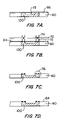
- FIGS. 7( a )– 7 ( d ) show cross-sections of a carrier in another process embodiment for forming a solder mask on the carrier.
- FIGS. 8( a )– 8 ( c ) show perspective views of semiconductor die package components. They are assembled together to form a semiconductor die package. In the illustrated process, the semiconductor die does not need to be bumped before being attached to the carrier. Rather, solder balls can be deposited simultaneously on the semiconductor die and the carrier.
- One embodiment of the invention is directed to a carrier comprising a die attach region and a plurality of edge regions. Each edge region can have a surface that is elevated with respect to the die attach region. Each edge region can also partially define the die attach region.
- the carrier may also comprise a base metal and one or more layers of material on the base metal. A first solder mask having one or more apertures is disposed on an edge region.
- a semiconductor die is attached to the die attach region of the carrier.
- the semiconductor die may have a MOSFET with a source region, a gate region, and a drain region.
- the drain region is proximate to the die attach region and the source region is distal to the die attach region.
- a second solder mask can be disposed on the semiconductor die.
- the second solder mask may comprise, for example, a silicon nitride layer with apertures. Metal connecting to the gate region or the source region may be exposed through the apertures in the second solder mask.
- a plurality of solder deposits are disposed within the one or more apertures in the first solder mask and the second solder mask. In some embodiments, the solder deposits can be solder balls.
- FIG. 1 shows a perspective view of an exemplary semiconductor die package 120 according to an embodiment of the invention.
- the semiconductor die package 120 has a carrier 100 and a semiconductor die 102 disposed on the carrier 100 .
- the semiconductor die 102 can comprise a semiconductor material such as silicon.
- An array of solder balls 108 is disposed on the semiconductor die 102 and two edge regions 106 ( a ), 106 ( b ) in the carrier 100 .
- the carrier 100 can be considered a lead frame.
- the carrier 100 can be both thermally and electrically conductive.
- the carrier 100 can comprise a body comprising a base metal such as copper or aluminum.
- the base metal may have one or more layers of material coated on it.
- the one or more layers of material may comprise any suitable underbump metallurgy combination.
- at least one of an adhesion layer, a barrier layer, a solder wettable layer, and an oxidation barrier layer may be formed on the base metal.
- the carrier base metal may comprise copper.
- the base metal may be coated with a nickel solder wettable layer and then a palladium or gold oxidation barrier layer.
- the semiconductor die 102 may comprise, for example, a vertical MOSFET device.
- the vertical MOSFET device has a source region, a drain region, and a gate region.
- the source region and the drain region are at opposite sides of the semiconductor die 102 so that current flows vertically through the semiconductor die 102 .
- a solder mask comprising, for example, silicon nitride may be formed over metal regions in the semiconductor die 102 . Apertures in the solder mask can be disposed over the metal regions so that solder deposits in the apertures contact the metal regions and communicate with the source and drain regions.
- the carrier 100 shown in FIG. 1 includes two edge regions 110 ( a ), 110 ( b ) that are disposed on opposite sides of the semiconductor die 102 .
- the edge regions 110 ( a ), 110 ( b ) have surfaces that are elevated above the die attach region of the carrier 100 .
- both edge regions 110 ( a ), 110 ( b ) at least partially define the die attach region of the carrier 100 .
- the upper surfaces of the edge regions 110 ( a ), 110 ( b ) are substantially coplanar with the upper surface of the semiconductor die 102 . Solder masks disposed on these surfaces can also be substantially coplanar.
- solder mask 110 ( a ) is disposed on one edge region 106 ( a ), while another solder mask 110 ( b ) is disposed on another edge region 106 ( b ).
- Each solder mask 110 ( a ), 110 ( b ) has one or more apertures.
- Each solder mask preferably comprises a material that has a melting temperature that is higher than the reflow temperature of the solder that deposited within its apertures.
- the solder mask comprises a polymeric material such as polyimide.
- the solder mask 110 helps to keep solder deposits (e.g., solder balls) confined to predetermined locations on the carrier 110 .
- the solder ball array 108 is divided into two groups; a first outer array of solder balls 108 - 1 that connects to carrier edge regions 106 and an internal array of solder balls 108 - 2 connecting to the surface of the semiconductor die 102 .
- the solder balls 108 - 1 disposed in apertures in the solder masks 110 ( a ), 110 ( b ) are substantially coplanar with the solder balls 108 - 2 on the semiconductor die 102 .
- an array 108 of solder balls is shown in FIG. 1
- the solder deposited within the apertures of the solder mask 110 may be, for example, columns or cones of solder.
- solder balls 108 - 1 provide the connection to the drain terminal of the device.
- Other solder balls 108 - 2 provide the connection to the source and gate terminals of the device.
- a corner solder ball 108 - 2 G is dedicated for the gate terminal and the remaining solder balls in the internal array 108 - 2 provide for a distributed, low resistance connection to the source terminal of the MOSFET.
- the combination of a highly conductive carrier 100 and the array of solder balls 108 - 1 plus a distributed array of solder balls 108 - 2 across the surface of the semiconductor die reduces the length of the current path through the metal connections.
- FIG. 2 is an exploded view of the semiconductor die package shown in FIG. 1 .
- like elements as shown in FIG. 1 are designated with like numerals.
- the die attach region 115 of the carrier 100 is more clearly visible.
- the die attach region 115 is between the two edge regions 106 ( a ), 106 ( b ) in the semiconductor die package.
- the carrier 100 may have one, three, four etc. distinct edge regions.
- the carrier 100 may have four edge regions that form a square recess (not shown). A semiconductor die may then inserted within the square recess.
- the semiconductor die 102 can be attached to the die attach region 115 using any one of a variety of well known die attach materials such as conductive epoxies, and soft or hard solder materials. After bonding the semiconductor die 102 to the carrier 100 , the bonding layer of epoxy or solder may form a bond line.
- the height of each of the edge regions 106 (relative to the die attach region) is substantially equal to the thickness of semiconductor die 102 plus the thickness of die attach bond line 104 . This ensures that the outer surface of die 102 and the edge regions 106 of carrier 100 surrounding the semiconductor die 102 form a uniform plane.
- the semiconductor die 102 and the carrier 100 can have any suitable dimensions.
- a typical semiconductor die may be, for example, about 0.008 inches thick (or less) and the thickness of carrier 100 at the bottom of the recess may be, for example, about 0.008 inches thick (or less). This results in an exemplary package that is about 0.4 millimeters thick (and about 0.6 millimeters thick with the solder balls) in some embodiments.
- the semiconductor die packages according to embodiments of the invention are particularly well suited for discrete products with high heat dissipation such as power switching devices (e.g., power MOSFETs) where an electrical connection to the back side of the die (MOSFET drain terminal) is required.
- power switching devices e.g., power MOSFETs
- MOSFET drain terminal an electrical connection to the back side of the die
- the semiconductor die packages according to embodiments of the invention provide for a very low resistance, compact connection between the back side of the die (the drain terminal of the power MOSFET) and a circuit substrate.
- a conductive carrier 100 for power MOSFET applications is used herein for illustrative purposes only, and that the carrier 100 may be made of a dielectric material such as dielectric ceramic material. Selective contact to the back side of the die is still possible with selective conductive traces through the ceramic carrier.
- FIG. 3 shows a flowchart of a process for forming the individual semiconductor dies that will be packaged.
- active or passive devices are formed in a semiconductor wafer (step 40 ).
- An example of an active device is a vertical MOSFET device.
- the MOSFET device may have a source region and a gate region (a planar or trenched gate) at one surface of the wafer and a drain region at the other surface of the wafer.
- the semiconductor wafer may have any suitable thickness including a thickness of about 15 to about 23 mils.
- solder mask with apertures is formed on the semiconductor wafer using conventional processes (step 42 ).
- the solder mask may comprise, for example, a dielectric material such as silicon nitride, glass, or silicon dioxide. Apertures in the solder mask may be disposed over metal regions that are respectively coupled to the source region(s) and the gate region(s) of the MOSFET device in the semiconductor wafer. Solder disposed in the apertures of the solder mask can contact the metal regions.
- FIG. 4 shows a portion of a semiconductor wafer after a solder mask 400 is formed on it.
- a source metal layer contacts n+ source regions.
- a drain metal connection is at the opposite side of the semiconductor wafer as the n+ source regions.
- a passivation layer 400 having a number of apertures may be formed over the source metal layer and may function as a solder mask Apertures 402 in the solder mask 400 expose the source metal underneath the solder mask 400 . Consequently, solder that is deposited within the apertures 402 can contact the source metal so that external contacts to the n+ source regions of the MOSFET device can be made.
- the semiconductor wafer can be subjected to a thinning process (step 44 ).
- the back surface of the semiconductor wafer can be lapped according to conventional processes.
- the semiconductor wafer may be thinned until it is about 4 to about 8 mils thick. Thinning the semiconductor wafer can improve the heat dissipation properties of semiconductor dies in the wafer. Heat can dissipate from thinner semiconductor dies more quickly than thicker semiconductor dies. Thinning also makes it easier to dice the wafer to form the individual semiconductor dies.
- the semiconductor wafer can be diced to form the individual semiconductor dies (step 46 ). Any suitable dicing process may be used. Exemplary dicing processes include wafer sawing, laser cutting, etc. Once the individual semiconductor dies are formed, they can be packaged.
- FIG. 5 shows a flowchart for a process for forming the semiconductor die packages according to embodiments of the invention.
- a carrier is formed (step 50 ).
- the carrier can be formed, for example, by stamping a metal sheet to form a die attach region and edge regions in the metal sheet.
- a flat metal sheet may be placed in a stamping apparatus to stamp the metal sheet and form the die attach region of the carrier.
- solder mask can be formed on the metal sheet and on an edge region of the carrier (step 52 ).
- the solder mask may comprise a heat resistant polymeric material such as polyimide.
- the solder mask is preferably formed using a photolithography process. The steps used in exemplary photolithography processes are described in further detail below.
- the solder masks may have any suitable form.
- a solder mask on the carrier may simply be a ring of material that confines a solder deposit to a predetermined location.
- the solder mask may be a layer with two or more apertures in it.
- one or more additional layers may be formed on the base metal of the carrier.
- the one or more additional layers may include adhesion layers, diffusion barriers, solder wettable layers, and oxidation barrier layers. Examples of materials that can be used in the one or more layers include Ni, Pd, Cr, Cu, Au, and alloys thereof. Any suitable process including electroplating, sputtering, electroless plating, etc. may be used to form the one or more additional layers of material on the base metal of the carrier.
- the solder masks can be formed on the base metal of a carrier after forming various layers on the base metal.
- a metal sheet 60 may comprise a die attach region 115 that partially defines a recess in the metal sheet 60 .
- the die attach region 115 may have been previously formed by stamping.
- One or more layers 64 of material may be deposited on the metal sheet 60 .
- the layers may comprise, for example, a solder wettable layer comprising nickel and an oxidation barrier layer comprising palladium.
- FIGS. 6( a ) to 6 ( d ) the outline of the carrier 100 that will eventually be formed from the metal sheet 60 is shown by cross-hatches. The cross-hatched region can be cut out at a later time.
- one side of the metal sheet 60 can be coated with one or more layers of material 64 . In other embodiments, both sides of the metal sheet 60 can be coated with one or more layers of material.
- a photosensitive layer 66 may be deposited on the metal sheet 60 .
- the photosensitive layer 66 may comprise a positive or a negative photosensitive material. Any suitable process may be used to deposit the photosensitive layer 66 .
- the photosensitive layer 66 can be laminated to the metal sheet 60 or may be printed on the metal sheet 60 . Any suitable material can be used in the photosensitive layer 66 .
- the photosensitive layer 66 comprises a polyimide or polyimide precursor. Many polyimides do not melt or decompose at high temperatures and can thus be left on the metal sheet 60 during a reflow process.
- a photomask 70 is disposed over the photosensitive layer 66 .
- the photomask 70 includes a number of regions that are transparent to radiation and a number of regions that are not transparent to radiation.
- the photosensitive layer 66 can thus be irradiated with a pattern of radiation passing through the photomask 70 .
- Radiation 74 can pass through the photomask 70 to render certain portions 72 of the photosensitive layer 66 insoluble to a developing solution. In some embodiments, portions of the photosensitive layer 66 that are not irradiated can be developed in the developing solution.
- the photosensitive layer 66 can be exposed to a developing solution to remove the non-irradiated portions of the photosensitive layer 66 .
- a solder mask 76 containing apertures can be disposed on the metal sheet 60 .
- a semiconductor die (not shown) can be bonded to the die attach region 115 of the carrier 100 .
- a solder mask can be formed on the base metal of a carrier before forming various underbump metallurgy layers on the carrier.
- a photosensitive layer 66 can be deposited onto a metal sheet 60 in the same or different manner as previously described.
- the metal sheet 60 has a recess that is partially defined by a die attach region 115 . Prior to receiving the photosensitive layer 66 , the metal sheet 60 may be uncoated.
- the photosensitive layer 66 after the photosensitive layer 66 is on the metal sheet 60 , it can be irradiated in the same or different manner as previously described. As shown in FIG. 7( c ), after irradiating the photosensitive layer 66 , the photosensitive layer 66 can be developed to leave a solder mask 76 with one or more apertures.
- one or more layers of material may be deposited on the metal sheet 60 .
- the one or more layers 64 of material may comprise the same or different layers, and may be deposited in the same or different manner, as described above. In this example, at least a portion of the one or more layers 64 of material are deposited within the apertures of the solder mask 76 .
- a semiconductor die (not shown) can be bonded to the die attach region 115 of the carrier 100 .
- the semiconductor die can be attached to the carrier.
- the semiconductor die 102 may be attached to the die attach region 115 using solder or a conductive adhesive (e.g., a conductive epoxy).
- Solder masks 110 ( a ), 110 ( b ) with apertures 110 - 1 may be disposed on the edge regions of the carrier 100 .
- a second solder mask 150 with apertures 150 - 1 can be in the semiconductor die 102 .
- solder balls 108 may be deposited in the apertures 110 - 1 in the first solder mask 110 on the carrier 100 and in the apertures 150 - 1 in the second solder mask 150 in the semiconductor die 102 .
- the solder balls 108 can alternatively be solder deposits such as solder columns or conical solder deposits.
- the solder balls 108 (or other type of solder deposit) used in embodiments of the invention may comprise any suitable material including Pb—Sn, In—Sn, etc. with atomic elements in any suitable atomic or weight proportions (e.g., 63/37, 95/5).
- the regions of the semiconductor die 102 exposed through the apertures 150 - 1 are solderable to enable simultaneous ball attach on the semiconductor die 102 and carrier 100 .
- the regions within or under the apertures 150 - 1 may contain aluminum and any suitable underbump metallurgy layers (such as those described above).
- Ni—Au can be sputtered or electrolessly plated within or under the apertures 150 - 1 on aluminum in the semiconductor die 102 to make the regions exposed by the apertures 150 - 1 solderable.
- the solder balls can be placed within the apertures of the solder masks on the semiconductor die 102 and on the edge regions of the carrier 100 by a pick and place process.
- solder can be deposited in the apertures of the solder masks using, for example, a screening process, electoplating process, or any other suitable process.
- a screening process a solder stencil can be placed over the semiconductor die 102 and the edge regions of the carrier 100 . Apertures in the stencil can correspond to the apertures in the first and the second solder masks.
- Solder paste can be screened or into the apertures of the solder stencil and into the apertures in the first and the second solder masks. Regardless of the particular solder deposition method used, the solder is preferably deposited in the apertures in the first and the second solder masks substantially simultaneously.
- the solder After depositing solder within the apertures first and second solder masks, the solder can be reflowed within the apertures in the first and the second solder masks.
- a full reflow process can be performed. In a typical reflow process, the solder can be heated above 150° C. for about 15 minutes or more. The particular reflow conditions will, however, depend on the particular solder being used, the particular package being formed, etc.
- the resulting semiconductor die package 120 can be as shown in FIG. 8( c ).
- the semiconductor die package 120 shown in FIG. 8( c ) can then be flipped over and mounted on the conductive lands of a circuit substrate (e.g., a circuit board).
- Embodiments of the invention have a number of advantages.
- solder can be deposited on the carrier and the semiconductor die in a single process step. Accordingly, solder contacts in the semiconductor die package can be made quickly and efficiently.
- embodiments of the invention reduce the likelihood that the solder deposits will not be coplanar in the formed die package, since all solder deposits in the package are processed in the same way and at the same time.
- a solder mask is used on the carrier so that a full reflow process can be performed on the solder on the carrier.
- the solder mask confines the deposited solder so that the solder deposits (e.g., solder balls) in the solder mask apertures do not substantially deform during reflow.
- solder deposits e.g., solder balls
- stronger bonds between the solder and the carrier can be formed than if the solder on the carrier is subjected to a partial reflow process.
- the solder mask(s) on the carrier need not contact the circuit substrate.
- the heat passing to the solder mask(s) on the carrier is minimized due to the gap between the solder mask and the circuit substrate. Consequently, any possible thermal degradation of the solder mask(s) is also minimized.
Abstract
Description
Claims (13)
Priority Applications (1)
| Application Number | Priority Date | Filing Date | Title |
|---|---|---|---|
| US10/455,511 US7157799B2 (en) | 2001-04-23 | 2003-06-04 | Semiconductor die package including carrier with mask and semiconductor die |
Applications Claiming Priority (2)
| Application Number | Priority Date | Filing Date | Title |
|---|---|---|---|
| US09/841,333 US6645791B2 (en) | 2001-04-23 | 2001-04-23 | Semiconductor die package including carrier with mask |
| US10/455,511 US7157799B2 (en) | 2001-04-23 | 2003-06-04 | Semiconductor die package including carrier with mask and semiconductor die |
Related Parent Applications (1)
| Application Number | Title | Priority Date | Filing Date |
|---|---|---|---|
| US09/841,333 Division US6645791B2 (en) | 2001-04-23 | 2001-04-23 | Semiconductor die package including carrier with mask |
Publications (2)
| Publication Number | Publication Date |
|---|---|
| US20030205798A1 US20030205798A1 (en) | 2003-11-06 |
| US7157799B2 true US7157799B2 (en) | 2007-01-02 |
Family
ID=25284599
Family Applications (2)
| Application Number | Title | Priority Date | Filing Date |
|---|---|---|---|
| US09/841,333 Expired - Fee Related US6645791B2 (en) | 2001-04-23 | 2001-04-23 | Semiconductor die package including carrier with mask |
| US10/455,511 Expired - Lifetime US7157799B2 (en) | 2001-04-23 | 2003-06-04 | Semiconductor die package including carrier with mask and semiconductor die |
Family Applications Before (1)
| Application Number | Title | Priority Date | Filing Date |
|---|---|---|---|
| US09/841,333 Expired - Fee Related US6645791B2 (en) | 2001-04-23 | 2001-04-23 | Semiconductor die package including carrier with mask |
Country Status (1)
| Country | Link |
|---|---|
| US (2) | US6645791B2 (en) |
Cited By (80)
| Publication number | Priority date | Publication date | Assignee | Title |
|---|---|---|---|---|
| US20060267155A1 (en) * | 2005-05-31 | 2006-11-30 | Takashi Ohsumi | Semiconductor wafer, and semiconductor device formed therefrom |
| US20070187807A1 (en) * | 2006-02-13 | 2007-08-16 | Jeongil Lee | Multi-chip module for battery power control |
| US20080054417A1 (en) * | 2006-08-29 | 2008-03-06 | Sangdo Lee | Semiconductor die package including stacked dice and heat sink structures |
| US20080173991A1 (en) * | 2007-01-24 | 2008-07-24 | Erwin Victor Cruz | Pre-molded clip structure |
| US20080185696A1 (en) * | 2007-02-05 | 2008-08-07 | Ruben Madrid | Semiconductor die package including leadframe with die attach pad with folded edge |
| US20080203559A1 (en) * | 2007-02-28 | 2008-08-28 | Lee Keun-Hyuk | Power device package and semiconductor package mold for fabricating the same |
| US20080224285A1 (en) * | 2007-03-12 | 2008-09-18 | Lim Seung-Won | Power module having stacked flip-chip and method of fabricating the power module |
| US20080251739A1 (en) * | 2007-04-13 | 2008-10-16 | Yoon Hwa Choi | Optical coupler package |
| US20080258272A1 (en) * | 2007-04-19 | 2008-10-23 | Lay Yeap Lim | Etched leadframe structure |
| US20090057854A1 (en) * | 2007-08-28 | 2009-03-05 | Gomez Jocel P | Self locking and aligning clip structure for semiconductor die package |
| US20090057852A1 (en) * | 2007-08-27 | 2009-03-05 | Madrid Ruben P | Thermally enhanced thin semiconductor package |
| US20090057855A1 (en) * | 2007-08-30 | 2009-03-05 | Maria Clemens Quinones | Semiconductor die package including stand off structures |
| US20090140266A1 (en) * | 2007-11-30 | 2009-06-04 | Yong Liu | Package including oriented devices |
| US20090140179A1 (en) * | 2007-11-30 | 2009-06-04 | Yong Liu | Semiconductor die packages suitable for optoelectronic applications having clip attach structures for angled mounting of dice |
| US20090160036A1 (en) * | 2007-12-19 | 2009-06-25 | David Grey | Package with multiple dies |
| US20090166826A1 (en) * | 2007-12-27 | 2009-07-02 | Janducayan Omar A | Lead frame die attach paddles with sloped walls and backside grooves suitable for leadless packages |
| US20090174048A1 (en) * | 2008-01-09 | 2009-07-09 | Yong Liu | Die package including substrate with molded device |
| US20090174044A1 (en) * | 2007-12-13 | 2009-07-09 | Eom Joo-Yang | Multi-chip package |
| US20090179313A1 (en) * | 2008-01-10 | 2009-07-16 | Maria Clemens Quinones | Flex clip connector for semiconductor device |
| US20090194857A1 (en) * | 2008-02-01 | 2009-08-06 | Yong Liu | Thin Compact Semiconductor Die Packages Suitable for Smart-Power Modules, Methods of Making the Same, and Systems Using the Same |
| US20090194856A1 (en) * | 2008-02-06 | 2009-08-06 | Gomez Jocel P | Molded package assembly |
| US20090218666A1 (en) * | 2008-02-28 | 2009-09-03 | Yang Gwi-Gyeon | Power device package and method of fabricating the same |
| US20090230536A1 (en) * | 2008-03-12 | 2009-09-17 | Yong Liu | Semiconductor die package including multiple semiconductor dice |
| US20090230537A1 (en) * | 2008-03-12 | 2009-09-17 | Yong Liu | Semiconductor die package including embedded flip chip |
| US20090243079A1 (en) * | 2008-03-31 | 2009-10-01 | Lim Seung-Won | Semiconductor device package |
| US20090278241A1 (en) * | 2008-05-08 | 2009-11-12 | Yong Liu | Semiconductor die package including die stacked on premolded substrate including die |
| US20100052119A1 (en) * | 2008-08-28 | 2010-03-04 | Yong Liu | Molded Ultra Thin Semiconductor Die Packages, Systems Using the Same, and Methods of Making the Same |
| US20100072590A1 (en) * | 2008-09-22 | 2010-03-25 | Yong Liu | Stacking Quad Pre-Molded Component Packages, Systems Using the Same, and Methods of Making the Same |
| US20100123257A1 (en) * | 2008-11-14 | 2010-05-20 | Yong Liu | Flexible and Stackable Semiconductor Die Packages, Systems Using the Same, and Methods of Making the Same |
| US7737548B2 (en) | 2007-08-29 | 2010-06-15 | Fairchild Semiconductor Corporation | Semiconductor die package including heat sinks |
| US20100148346A1 (en) * | 2008-12-12 | 2010-06-17 | Quinones Maria Clemens Y | Semiconductor die package including low stress configuration |
| US20100193921A1 (en) * | 2009-02-05 | 2010-08-05 | Jereza Armand Vincent C | Semiconductor die package and method for making the same |
| US20100193803A1 (en) * | 2009-02-04 | 2010-08-05 | Yong Liu | Stacked Micro Optocouplers and Methods of Making the Same |
| US7791084B2 (en) | 2008-01-09 | 2010-09-07 | Fairchild Semiconductor Corporation | Package with overlapping devices |
| WO2010147934A1 (en) * | 2009-06-16 | 2010-12-23 | Hsio Technologies, Llc | Semiconductor die terminal |
| US20110221072A1 (en) * | 2010-03-09 | 2011-09-15 | Chee Keong Chin | Integrated circuit packaging system with via and method of manufacture thereof |
| US8193618B2 (en) | 2008-12-12 | 2012-06-05 | Fairchild Semiconductor Corporation | Semiconductor die package with clip interconnection |
| US8421204B2 (en) | 2011-05-18 | 2013-04-16 | Fairchild Semiconductor Corporation | Embedded semiconductor power modules and packages |
| US8525346B2 (en) | 2009-06-02 | 2013-09-03 | Hsio Technologies, Llc | Compliant conductive nano-particle electrical interconnect |
| US8610265B2 (en) | 2009-06-02 | 2013-12-17 | Hsio Technologies, Llc | Compliant core peripheral lead semiconductor test socket |
| US8618649B2 (en) | 2009-06-02 | 2013-12-31 | Hsio Technologies, Llc | Compliant printed circuit semiconductor package |
| US8758067B2 (en) | 2010-06-03 | 2014-06-24 | Hsio Technologies, Llc | Selective metalization of electrical connector or socket housing |
| US8789272B2 (en) | 2009-06-02 | 2014-07-29 | Hsio Technologies, Llc | Method of making a compliant printed circuit peripheral lead semiconductor test socket |
| US8803539B2 (en) | 2009-06-03 | 2014-08-12 | Hsio Technologies, Llc | Compliant wafer level probe assembly |
| US8912812B2 (en) | 2009-06-02 | 2014-12-16 | Hsio Technologies, Llc | Compliant printed circuit wafer probe diagnostic tool |
| US8928344B2 (en) | 2009-06-02 | 2015-01-06 | Hsio Technologies, Llc | Compliant printed circuit socket diagnostic tool |
| US8955215B2 (en) | 2009-05-28 | 2015-02-17 | Hsio Technologies, Llc | High performance surface mount electrical interconnect |
| US8955216B2 (en) | 2009-06-02 | 2015-02-17 | Hsio Technologies, Llc | Method of making a compliant printed circuit peripheral lead semiconductor package |
| US8981568B2 (en) | 2009-06-16 | 2015-03-17 | Hsio Technologies, Llc | Simulated wirebond semiconductor package |
| US8981809B2 (en) | 2009-06-29 | 2015-03-17 | Hsio Technologies, Llc | Compliant printed circuit semiconductor tester interface |
| US8988093B2 (en) | 2009-06-02 | 2015-03-24 | Hsio Technologies, Llc | Bumped semiconductor wafer or die level electrical interconnect |
| US8987886B2 (en) | 2009-06-02 | 2015-03-24 | Hsio Technologies, Llc | Copper pillar full metal via electrical circuit structure |
| US8984748B2 (en) | 2009-06-29 | 2015-03-24 | Hsio Technologies, Llc | Singulated semiconductor device separable electrical interconnect |
| US9054097B2 (en) | 2009-06-02 | 2015-06-09 | Hsio Technologies, Llc | Compliant printed circuit area array semiconductor device package |
| US9093767B2 (en) | 2009-06-02 | 2015-07-28 | Hsio Technologies, Llc | High performance surface mount electrical interconnect |
| US9136196B2 (en) | 2009-06-02 | 2015-09-15 | Hsio Technologies, Llc | Compliant printed circuit wafer level semiconductor package |
| US9184145B2 (en) | 2009-06-02 | 2015-11-10 | Hsio Technologies, Llc | Semiconductor device package adapter |
| US9184527B2 (en) | 2009-06-02 | 2015-11-10 | Hsio Technologies, Llc | Electrical connector insulator housing |
| US9196980B2 (en) | 2009-06-02 | 2015-11-24 | Hsio Technologies, Llc | High performance surface mount electrical interconnect with external biased normal force loading |
| US9232654B2 (en) | 2009-06-02 | 2016-01-05 | Hsio Technologies, Llc | High performance electrical circuit structure |
| US9231328B2 (en) | 2009-06-02 | 2016-01-05 | Hsio Technologies, Llc | Resilient conductive electrical interconnect |
| US9277654B2 (en) | 2009-06-02 | 2016-03-01 | Hsio Technologies, Llc | Composite polymer-metal electrical contacts |
| US9276336B2 (en) | 2009-05-28 | 2016-03-01 | Hsio Technologies, Llc | Metalized pad to electrical contact interface |
| US9276339B2 (en) | 2009-06-02 | 2016-03-01 | Hsio Technologies, Llc | Electrical interconnect IC device socket |
| US9320133B2 (en) | 2009-06-02 | 2016-04-19 | Hsio Technologies, Llc | Electrical interconnect IC device socket |
| US9320144B2 (en) | 2009-06-17 | 2016-04-19 | Hsio Technologies, Llc | Method of forming a semiconductor socket |
| US9318862B2 (en) | 2009-06-02 | 2016-04-19 | Hsio Technologies, Llc | Method of making an electronic interconnect |
| US9350093B2 (en) | 2010-06-03 | 2016-05-24 | Hsio Technologies, Llc | Selective metalization of electrical connector or socket housing |
| US9414500B2 (en) | 2009-06-02 | 2016-08-09 | Hsio Technologies, Llc | Compliant printed flexible circuit |
| US9536815B2 (en) | 2009-05-28 | 2017-01-03 | Hsio Technologies, Llc | Semiconductor socket with direct selective metalization |
| US9559447B2 (en) | 2015-03-18 | 2017-01-31 | Hsio Technologies, Llc | Mechanical contact retention within an electrical connector |
| US9603249B2 (en) | 2009-06-02 | 2017-03-21 | Hsio Technologies, Llc | Direct metalization of electrical circuit structures |
| US9613841B2 (en) | 2009-06-02 | 2017-04-04 | Hsio Technologies, Llc | Area array semiconductor device package interconnect structure with optional package-to-package or flexible circuit to package connection |
| US9689897B2 (en) | 2010-06-03 | 2017-06-27 | Hsio Technologies, Llc | Performance enhanced semiconductor socket |
| US9699906B2 (en) | 2009-06-02 | 2017-07-04 | Hsio Technologies, Llc | Hybrid printed circuit assembly with low density main core and embedded high density circuit regions |
| US9761520B2 (en) | 2012-07-10 | 2017-09-12 | Hsio Technologies, Llc | Method of making an electrical connector having electrodeposited terminals |
| US9930775B2 (en) | 2009-06-02 | 2018-03-27 | Hsio Technologies, Llc | Copper pillar full metal via electrical circuit structure |
| US10159154B2 (en) | 2010-06-03 | 2018-12-18 | Hsio Technologies, Llc | Fusion bonded liquid crystal polymer circuit structure |
| US10506722B2 (en) | 2013-07-11 | 2019-12-10 | Hsio Technologies, Llc | Fusion bonded liquid crystal polymer electrical circuit structure |
| US10667410B2 (en) | 2013-07-11 | 2020-05-26 | Hsio Technologies, Llc | Method of making a fusion bonded circuit structure |
Families Citing this family (39)
| Publication number | Priority date | Publication date | Assignee | Title |
|---|---|---|---|---|
| US6989588B2 (en) * | 2000-04-13 | 2006-01-24 | Fairchild Semiconductor Corporation | Semiconductor device including molded wireless exposed drain packaging |
| US6870254B1 (en) * | 2000-04-13 | 2005-03-22 | Fairchild Semiconductor Corporation | Flip clip attach and copper clip attach on MOSFET device |
| US20020173077A1 (en) * | 2001-05-03 | 2002-11-21 | Ho Tzong Da | Thermally enhanced wafer-level chip scale package and method of fabricating the same |
| US6893901B2 (en) * | 2001-05-14 | 2005-05-17 | Fairchild Semiconductor Corporation | Carrier with metal bumps for semiconductor die packages |
| US6867489B1 (en) * | 2002-01-22 | 2005-03-15 | Fairchild Semiconductor Corporation | Semiconductor die package processable at the wafer level |
| US7122884B2 (en) * | 2002-04-16 | 2006-10-17 | Fairchild Semiconductor Corporation | Robust leaded molded packages and methods for forming the same |
| KR101075169B1 (en) * | 2003-08-27 | 2011-10-19 | 페어차일드코리아반도체 주식회사 | Power module flip chip package |
| US8368223B2 (en) * | 2003-10-24 | 2013-02-05 | International Rectifier Corporation | Paste for forming an interconnect and interconnect formed from the paste |
| US7315081B2 (en) * | 2003-10-24 | 2008-01-01 | International Rectifier Corporation | Semiconductor device package utilizing proud interconnect material |
| US7196313B2 (en) * | 2004-04-02 | 2007-03-27 | Fairchild Semiconductor Corporation | Surface mount multi-channel optocoupler |
| JP2006210777A (en) * | 2005-01-31 | 2006-08-10 | Nec Electronics Corp | Semiconductor device |
| US7417312B2 (en) * | 2005-04-22 | 2008-08-26 | International Rectifier Corporation | Use of solder paste for heat dissipation |
| US7202113B2 (en) * | 2005-06-09 | 2007-04-10 | Ming Sun | Wafer level bumpless method of making a flip chip mounted semiconductor device package |
| JP2006352008A (en) * | 2005-06-20 | 2006-12-28 | Nec Electronics Corp | Semiconductor device and circuit substrate |
| KR101297645B1 (en) | 2005-06-30 | 2013-08-20 | 페어차일드 세미컨덕터 코포레이션 | Semiconductor die package and method for making the same |
| US7504733B2 (en) | 2005-08-17 | 2009-03-17 | Ciclon Semiconductor Device Corp. | Semiconductor die package |
| US7560808B2 (en) * | 2005-10-19 | 2009-07-14 | Texas Instruments Incorporated | Chip scale power LDMOS device |
| US7285849B2 (en) * | 2005-11-18 | 2007-10-23 | Fairchild Semiconductor Corporation | Semiconductor die package using leadframe and clip and method of manufacturing |
| US7371616B2 (en) * | 2006-01-05 | 2008-05-13 | Fairchild Semiconductor Corporation | Clipless and wireless semiconductor die package and method for making the same |
| US20070164428A1 (en) * | 2006-01-18 | 2007-07-19 | Alan Elbanhawy | High power module with open frame package |
| US7446375B2 (en) * | 2006-03-14 | 2008-11-04 | Ciclon Semiconductor Device Corp. | Quasi-vertical LDMOS device having closed cell layout |
| US20070215997A1 (en) * | 2006-03-17 | 2007-09-20 | Martin Standing | Chip-scale package |
| US7768075B2 (en) | 2006-04-06 | 2010-08-03 | Fairchild Semiconductor Corporation | Semiconductor die packages using thin dies and metal substrates |
| US7656024B2 (en) * | 2006-06-30 | 2010-02-02 | Fairchild Semiconductor Corporation | Chip module for complete power train |
| US20080036078A1 (en) * | 2006-08-14 | 2008-02-14 | Ciclon Semiconductor Device Corp. | Wirebond-less semiconductor package |
| US20090160039A1 (en) * | 2007-12-20 | 2009-06-25 | National Semiconductor Corporation | Method and leadframe for packaging integrated circuits |
| US7825502B2 (en) * | 2008-01-09 | 2010-11-02 | Fairchild Semiconductor Corporation | Semiconductor die packages having overlapping dice, system using the same, and methods of making the same |
| US7745244B2 (en) | 2008-06-23 | 2010-06-29 | Fairchild Semiconductor Corporation | Pin substrate and package |
| US8164179B2 (en) * | 2008-12-16 | 2012-04-24 | STMicroelectronics Asia Pacific PTE Ltd-Singapore | Chip scale package structure with can attachment |
| US8049312B2 (en) * | 2009-01-12 | 2011-11-01 | Texas Instruments Incorporated | Semiconductor device package and method of assembly thereof |
| US20100289129A1 (en) * | 2009-05-14 | 2010-11-18 | Satya Chinnusamy | Copper plate bonding for high performance semiconductor packaging |
| TWI463620B (en) * | 2012-08-22 | 2014-12-01 | 矽品精密工業股份有限公司 | Method of forming package substrate |
| US9812380B2 (en) * | 2014-05-22 | 2017-11-07 | Microchip Technology Incorporated | Bumps bonds formed as metal line interconnects in a semiconductor device |
| CN105448871B (en) * | 2014-08-18 | 2019-03-08 | 万国半导体股份有限公司 | Power semiconductor and preparation method |
| US9337131B2 (en) * | 2014-09-29 | 2016-05-10 | Alpha And Omega Semiconductor (Cayman) Ltd. | Power semiconductor device and the preparation method |
| DE102015120647B4 (en) * | 2015-11-27 | 2017-12-28 | Snaptrack, Inc. | Electrical device with thin solder stop layer and method of manufacture |
| WO2018004686A1 (en) * | 2016-07-01 | 2018-01-04 | Intel Corporation | Device, method and system for providing recessed interconnect structures of a substrate |
| CN107993991A (en) * | 2017-12-20 | 2018-05-04 | 合肥矽迈微电子科技有限公司 | A kind of chip-packaging structure and its manufacture method |
| US20200135632A1 (en) * | 2018-10-24 | 2020-04-30 | Texas Instruments Incorporated | Die isolation on a substrate |
Citations (16)
| Publication number | Priority date | Publication date | Assignee | Title |
|---|---|---|---|---|
| US4720915A (en) * | 1986-03-25 | 1988-01-26 | True Grid, Ltd. | Printed circuit board and process for its manufacture |
| US5027191A (en) * | 1989-05-11 | 1991-06-25 | Westinghouse Electric Corp. | Cavity-down chip carrier with pad grid array |
| US5583378A (en) * | 1994-05-16 | 1996-12-10 | Amkor Electronics, Inc. | Ball grid array integrated circuit package with thermal conductor |
| US5767575A (en) * | 1995-10-17 | 1998-06-16 | Prolinx Labs Corporation | Ball grid array structure and method for packaging an integrated circuit chip |
| US6034427A (en) * | 1998-01-28 | 2000-03-07 | Prolinx Labs Corporation | Ball grid array structure and method for packaging an integrated circuit chip |
| US6133634A (en) * | 1998-08-05 | 2000-10-17 | Fairchild Semiconductor Corporation | High performance flip chip package |
| US6201305B1 (en) | 2000-06-09 | 2001-03-13 | Amkor Technology, Inc. | Making solder ball mounting pads on substrates |
| US6249041B1 (en) * | 1998-06-02 | 2001-06-19 | Siliconix Incorporated | IC chip package with directly connected leads |
| US20010013654A1 (en) | 1998-12-31 | 2001-08-16 | Navinchandra Kalidas | Ball grid package with multiple power/ ground planes |
| US6284566B1 (en) | 1996-05-17 | 2001-09-04 | National Semiconductor Corporation | Chip scale package and method for manufacture thereof |
| US20010050441A1 (en) * | 2000-03-17 | 2001-12-13 | International Rectifier Corp. | Semiconductor multichip module package with improved thermal performance; reduced size and improved moisture resistance |
| US20020009826A1 (en) | 2000-04-14 | 2002-01-24 | Ray Chien | Method of manufacturing a cavity-down plastic ball grid array (CD-PBGA) substrate |
| US6392290B1 (en) | 2000-04-07 | 2002-05-21 | Siliconix Incorporated | Vertical structure for semiconductor wafer-level chip scale packages |
| US6544812B1 (en) * | 2000-11-06 | 2003-04-08 | St Assembly Test Service Ltd. | Single unit automated assembly of flex enhanced ball grid array packages |
| US6593168B1 (en) * | 2000-02-03 | 2003-07-15 | Advanced Micro Devices, Inc. | Method and apparatus for accurate alignment of integrated circuit in flip-chip configuration |
| US6661082B1 (en) | 2000-07-19 | 2003-12-09 | Fairchild Semiconductor Corporation | Flip chip substrate design |
-
2001
- 2001-04-23 US US09/841,333 patent/US6645791B2/en not_active Expired - Fee Related
-
2003
- 2003-06-04 US US10/455,511 patent/US7157799B2/en not_active Expired - Lifetime
Patent Citations (18)
| Publication number | Priority date | Publication date | Assignee | Title |
|---|---|---|---|---|
| US4720915A (en) * | 1986-03-25 | 1988-01-26 | True Grid, Ltd. | Printed circuit board and process for its manufacture |
| US5027191A (en) * | 1989-05-11 | 1991-06-25 | Westinghouse Electric Corp. | Cavity-down chip carrier with pad grid array |
| US5583378A (en) * | 1994-05-16 | 1996-12-10 | Amkor Electronics, Inc. | Ball grid array integrated circuit package with thermal conductor |
| US5767575A (en) * | 1995-10-17 | 1998-06-16 | Prolinx Labs Corporation | Ball grid array structure and method for packaging an integrated circuit chip |
| US6284566B1 (en) | 1996-05-17 | 2001-09-04 | National Semiconductor Corporation | Chip scale package and method for manufacture thereof |
| US6034427A (en) * | 1998-01-28 | 2000-03-07 | Prolinx Labs Corporation | Ball grid array structure and method for packaging an integrated circuit chip |
| US6249041B1 (en) * | 1998-06-02 | 2001-06-19 | Siliconix Incorporated | IC chip package with directly connected leads |
| US6133634A (en) * | 1998-08-05 | 2000-10-17 | Fairchild Semiconductor Corporation | High performance flip chip package |
| US20010013654A1 (en) | 1998-12-31 | 2001-08-16 | Navinchandra Kalidas | Ball grid package with multiple power/ ground planes |
| US6396136B2 (en) * | 1998-12-31 | 2002-05-28 | Texas Instruments Incorporated | Ball grid package with multiple power/ground planes |
| US6593168B1 (en) * | 2000-02-03 | 2003-07-15 | Advanced Micro Devices, Inc. | Method and apparatus for accurate alignment of integrated circuit in flip-chip configuration |
| US20010050441A1 (en) * | 2000-03-17 | 2001-12-13 | International Rectifier Corp. | Semiconductor multichip module package with improved thermal performance; reduced size and improved moisture resistance |
| US6392290B1 (en) | 2000-04-07 | 2002-05-21 | Siliconix Incorporated | Vertical structure for semiconductor wafer-level chip scale packages |
| US20020009826A1 (en) | 2000-04-14 | 2002-01-24 | Ray Chien | Method of manufacturing a cavity-down plastic ball grid array (CD-PBGA) substrate |
| US6566166B2 (en) * | 2000-04-14 | 2003-05-20 | Via Technologies Inc. | Method of manufacturing a cavity-down plastic ball grid array (CD-PBGA) substrate |
| US6201305B1 (en) | 2000-06-09 | 2001-03-13 | Amkor Technology, Inc. | Making solder ball mounting pads on substrates |
| US6661082B1 (en) | 2000-07-19 | 2003-12-09 | Fairchild Semiconductor Corporation | Flip chip substrate design |
| US6544812B1 (en) * | 2000-11-06 | 2003-04-08 | St Assembly Test Service Ltd. | Single unit automated assembly of flex enhanced ball grid array packages |
Cited By (130)
| Publication number | Priority date | Publication date | Assignee | Title |
|---|---|---|---|---|
| US8164164B2 (en) | 2005-05-31 | 2012-04-24 | Oki Semiconductor Co., Ltd. | Semiconductor wafer, and semiconductor device formed therefrom |
| US7915746B2 (en) * | 2005-05-31 | 2011-03-29 | Oki Semiconductor Co., Ltd. | Semiconductor wafer, and semiconductor device formed therefrom |
| US20060267155A1 (en) * | 2005-05-31 | 2006-11-30 | Takashi Ohsumi | Semiconductor wafer, and semiconductor device formed therefrom |
| US20110006438A1 (en) * | 2005-05-31 | 2011-01-13 | Oki Semiconductor Co., Ltd. | Semiconductor wafer, and semiconductor device formed therefrom |
| US7868432B2 (en) | 2006-02-13 | 2011-01-11 | Fairchild Semiconductor Corporation | Multi-chip module for battery power control |
| US20070187807A1 (en) * | 2006-02-13 | 2007-08-16 | Jeongil Lee | Multi-chip module for battery power control |
| US20080054417A1 (en) * | 2006-08-29 | 2008-03-06 | Sangdo Lee | Semiconductor die package including stacked dice and heat sink structures |
| US7564124B2 (en) | 2006-08-29 | 2009-07-21 | Fairchild Semiconductor Corporation | Semiconductor die package including stacked dice and heat sink structures |
| US20100258924A1 (en) * | 2007-01-24 | 2010-10-14 | Erwin Victor Cruz | Pre-molded clip structure |
| US7838340B2 (en) | 2007-01-24 | 2010-11-23 | Fairchild Semiconductor Corporation | Pre-molded clip structure |
| US7768105B2 (en) | 2007-01-24 | 2010-08-03 | Fairchild Semiconductor Corporation | Pre-molded clip structure |
| US20100258923A1 (en) * | 2007-01-24 | 2010-10-14 | Erwin Victor Cruz | Pre-molded clip structure |
| US8008759B2 (en) | 2007-01-24 | 2011-08-30 | Fairchild Semiconductor Corporation | Pre-molded clip structure |
| US9583454B2 (en) | 2007-01-24 | 2017-02-28 | Fairchild Semiconductor Corporation | Semiconductor die package including low stress configuration |
| US20080173991A1 (en) * | 2007-01-24 | 2008-07-24 | Erwin Victor Cruz | Pre-molded clip structure |
| US8513059B2 (en) | 2007-01-24 | 2013-08-20 | Fairchild Semiconductor Corporation | Pre-molded clip structure |
| US7821116B2 (en) | 2007-02-05 | 2010-10-26 | Fairchild Semiconductor Corporation | Semiconductor die package including leadframe with die attach pad with folded edge |
| US20110008935A1 (en) * | 2007-02-05 | 2011-01-13 | Fairchild Semiconductor Corporation | Semiconductor die package including leadframe with die attach pad with folded edge |
| US20080185696A1 (en) * | 2007-02-05 | 2008-08-07 | Ruben Madrid | Semiconductor die package including leadframe with die attach pad with folded edge |
| US8258622B2 (en) | 2007-02-28 | 2012-09-04 | Fairchild Korea Semiconductor, Ltd. | Power device package and semiconductor package mold for fabricating the same |
| US20080203559A1 (en) * | 2007-02-28 | 2008-08-28 | Lee Keun-Hyuk | Power device package and semiconductor package mold for fabricating the same |
| US20080224285A1 (en) * | 2007-03-12 | 2008-09-18 | Lim Seung-Won | Power module having stacked flip-chip and method of fabricating the power module |
| US9130065B2 (en) | 2007-03-12 | 2015-09-08 | Fairchild Korea Semiconductor, Ltd | Power module having stacked flip-chip and method for fabricating the power module |
| US7675148B2 (en) | 2007-03-12 | 2010-03-09 | Fairchild Korea Semiconductor Ltd. | Power module having stacked flip-chip and method of fabricating the power module |
| US7659531B2 (en) | 2007-04-13 | 2010-02-09 | Fairchild Semiconductor Corporation | Optical coupler package |
| US20080251739A1 (en) * | 2007-04-13 | 2008-10-16 | Yoon Hwa Choi | Optical coupler package |
| US20080258272A1 (en) * | 2007-04-19 | 2008-10-23 | Lay Yeap Lim | Etched leadframe structure |
| US7683463B2 (en) | 2007-04-19 | 2010-03-23 | Fairchild Semiconductor Corporation | Etched leadframe structure including recesses |
| US20090057852A1 (en) * | 2007-08-27 | 2009-03-05 | Madrid Ruben P | Thermally enhanced thin semiconductor package |
| US20110076807A1 (en) * | 2007-08-28 | 2011-03-31 | Gomez Jocel P | Self locking and aligning clip structure for semiconductor die package |
| US20090057854A1 (en) * | 2007-08-28 | 2009-03-05 | Gomez Jocel P | Self locking and aligning clip structure for semiconductor die package |
| US7902657B2 (en) | 2007-08-28 | 2011-03-08 | Fairchild Semiconductor Corporation | Self locking and aligning clip structure for semiconductor die package |
| US8067273B2 (en) | 2007-08-28 | 2011-11-29 | Fairchild Semiconductor Corporation | Self locking and aligning clip structure for semiconductor die package |
| US7737548B2 (en) | 2007-08-29 | 2010-06-15 | Fairchild Semiconductor Corporation | Semiconductor die package including heat sinks |
| US20090057855A1 (en) * | 2007-08-30 | 2009-03-05 | Maria Clemens Quinones | Semiconductor die package including stand off structures |
| US20090140266A1 (en) * | 2007-11-30 | 2009-06-04 | Yong Liu | Package including oriented devices |
| US20090140179A1 (en) * | 2007-11-30 | 2009-06-04 | Yong Liu | Semiconductor die packages suitable for optoelectronic applications having clip attach structures for angled mounting of dice |
| US7589338B2 (en) | 2007-11-30 | 2009-09-15 | Fairchild Semiconductor Corporation | Semiconductor die packages suitable for optoelectronic applications having clip attach structures for angled mounting of dice |
| US20090174044A1 (en) * | 2007-12-13 | 2009-07-09 | Eom Joo-Yang | Multi-chip package |
| US7936054B2 (en) | 2007-12-13 | 2011-05-03 | Fairchild Korea Semiconductor Ltd. | Multi-chip package |
| US20090160036A1 (en) * | 2007-12-19 | 2009-06-25 | David Grey | Package with multiple dies |
| US7781872B2 (en) | 2007-12-19 | 2010-08-24 | Fairchild Semiconductor Corporation | Package with multiple dies |
| US20090166826A1 (en) * | 2007-12-27 | 2009-07-02 | Janducayan Omar A | Lead frame die attach paddles with sloped walls and backside grooves suitable for leadless packages |
| US8106406B2 (en) | 2008-01-09 | 2012-01-31 | Fairchild Semiconductor Corporation | Die package including substrate with molded device |
| US7791084B2 (en) | 2008-01-09 | 2010-09-07 | Fairchild Semiconductor Corporation | Package with overlapping devices |
| US20090174048A1 (en) * | 2008-01-09 | 2009-07-09 | Yong Liu | Die package including substrate with molded device |
| US8525192B2 (en) | 2008-01-09 | 2013-09-03 | Fairchild Semiconductor Corporation | Die package including substrate with molded device |
| US20090311832A1 (en) * | 2008-01-10 | 2009-12-17 | Quinones Maria Clemens Y | Flex Chip Connector For Semiconductor Device |
| US7824966B2 (en) | 2008-01-10 | 2010-11-02 | Fairchild Semiconductor Corporation | Flex chip connector for semiconductor device |
| US20090179313A1 (en) * | 2008-01-10 | 2009-07-16 | Maria Clemens Quinones | Flex clip connector for semiconductor device |
| US7626249B2 (en) | 2008-01-10 | 2009-12-01 | Fairchild Semiconductor Corporation | Flex clip connector for semiconductor device |
| US20090194857A1 (en) * | 2008-02-01 | 2009-08-06 | Yong Liu | Thin Compact Semiconductor Die Packages Suitable for Smart-Power Modules, Methods of Making the Same, and Systems Using the Same |
| US20090194856A1 (en) * | 2008-02-06 | 2009-08-06 | Gomez Jocel P | Molded package assembly |
| US8198139B2 (en) | 2008-02-28 | 2012-06-12 | Fairchild Korea Semiconductor Ltd. | Power device package and method of fabricating the same |
| US20090218666A1 (en) * | 2008-02-28 | 2009-09-03 | Yang Gwi-Gyeon | Power device package and method of fabricating the same |
| US20090230537A1 (en) * | 2008-03-12 | 2009-09-17 | Yong Liu | Semiconductor die package including embedded flip chip |
| US20090230536A1 (en) * | 2008-03-12 | 2009-09-17 | Yong Liu | Semiconductor die package including multiple semiconductor dice |
| US8018054B2 (en) | 2008-03-12 | 2011-09-13 | Fairchild Semiconductor Corporation | Semiconductor die package including multiple semiconductor dice |
| US7768108B2 (en) | 2008-03-12 | 2010-08-03 | Fairchild Semiconductor Corporation | Semiconductor die package including embedded flip chip |
| US20090243079A1 (en) * | 2008-03-31 | 2009-10-01 | Lim Seung-Won | Semiconductor device package |
| US20090278241A1 (en) * | 2008-05-08 | 2009-11-12 | Yong Liu | Semiconductor die package including die stacked on premolded substrate including die |
| US20100052119A1 (en) * | 2008-08-28 | 2010-03-04 | Yong Liu | Molded Ultra Thin Semiconductor Die Packages, Systems Using the Same, and Methods of Making the Same |
| US7855439B2 (en) | 2008-08-28 | 2010-12-21 | Fairchild Semiconductor Corporation | Molded ultra thin semiconductor die packages, systems using the same, and methods of making the same |
| US20100072590A1 (en) * | 2008-09-22 | 2010-03-25 | Yong Liu | Stacking Quad Pre-Molded Component Packages, Systems Using the Same, and Methods of Making the Same |
| US7829988B2 (en) | 2008-09-22 | 2010-11-09 | Fairchild Semiconductor Corporation | Stacking quad pre-molded component packages, systems using the same, and methods of making the same |
| US8314499B2 (en) | 2008-11-14 | 2012-11-20 | Fairchild Semiconductor Corporation | Flexible and stackable semiconductor die packages having thin patterned conductive layers |
| US20100123257A1 (en) * | 2008-11-14 | 2010-05-20 | Yong Liu | Flexible and Stackable Semiconductor Die Packages, Systems Using the Same, and Methods of Making the Same |
| US20100148346A1 (en) * | 2008-12-12 | 2010-06-17 | Quinones Maria Clemens Y | Semiconductor die package including low stress configuration |
| US8193618B2 (en) | 2008-12-12 | 2012-06-05 | Fairchild Semiconductor Corporation | Semiconductor die package with clip interconnection |
| US8106501B2 (en) | 2008-12-12 | 2012-01-31 | Fairchild Semiconductor Corporation | Semiconductor die package including low stress configuration |
| US7973393B2 (en) | 2009-02-04 | 2011-07-05 | Fairchild Semiconductor Corporation | Stacked micro optocouplers and methods of making the same |
| US20100193803A1 (en) * | 2009-02-04 | 2010-08-05 | Yong Liu | Stacked Micro Optocouplers and Methods of Making the Same |
| US8222718B2 (en) | 2009-02-05 | 2012-07-17 | Fairchild Semiconductor Corporation | Semiconductor die package and method for making the same |
| US20100193921A1 (en) * | 2009-02-05 | 2010-08-05 | Jereza Armand Vincent C | Semiconductor die package and method for making the same |
| US9536815B2 (en) | 2009-05-28 | 2017-01-03 | Hsio Technologies, Llc | Semiconductor socket with direct selective metalization |
| US9276336B2 (en) | 2009-05-28 | 2016-03-01 | Hsio Technologies, Llc | Metalized pad to electrical contact interface |
| US9660368B2 (en) | 2009-05-28 | 2017-05-23 | Hsio Technologies, Llc | High performance surface mount electrical interconnect |
| US8955215B2 (en) | 2009-05-28 | 2015-02-17 | Hsio Technologies, Llc | High performance surface mount electrical interconnect |
| US8912812B2 (en) | 2009-06-02 | 2014-12-16 | Hsio Technologies, Llc | Compliant printed circuit wafer probe diagnostic tool |
| US8987886B2 (en) | 2009-06-02 | 2015-03-24 | Hsio Technologies, Llc | Copper pillar full metal via electrical circuit structure |
| US8704377B2 (en) | 2009-06-02 | 2014-04-22 | Hsio Technologies, Llc | Compliant conductive nano-particle electrical interconnect |
| US10609819B2 (en) | 2009-06-02 | 2020-03-31 | Hsio Technologies, Llc | Hybrid printed circuit assembly with low density main core and embedded high density circuit regions |
| US8789272B2 (en) | 2009-06-02 | 2014-07-29 | Hsio Technologies, Llc | Method of making a compliant printed circuit peripheral lead semiconductor test socket |
| US9320133B2 (en) | 2009-06-02 | 2016-04-19 | Hsio Technologies, Llc | Electrical interconnect IC device socket |
| US8829671B2 (en) | 2009-06-02 | 2014-09-09 | Hsio Technologies, Llc | Compliant core peripheral lead semiconductor socket |
| US8610265B2 (en) | 2009-06-02 | 2013-12-17 | Hsio Technologies, Llc | Compliant core peripheral lead semiconductor test socket |
| US8928344B2 (en) | 2009-06-02 | 2015-01-06 | Hsio Technologies, Llc | Compliant printed circuit socket diagnostic tool |
| US9930775B2 (en) | 2009-06-02 | 2018-03-27 | Hsio Technologies, Llc | Copper pillar full metal via electrical circuit structure |
| US8955216B2 (en) | 2009-06-02 | 2015-02-17 | Hsio Technologies, Llc | Method of making a compliant printed circuit peripheral lead semiconductor package |
| US9699906B2 (en) | 2009-06-02 | 2017-07-04 | Hsio Technologies, Llc | Hybrid printed circuit assembly with low density main core and embedded high density circuit regions |
| US8618649B2 (en) | 2009-06-02 | 2013-12-31 | Hsio Technologies, Llc | Compliant printed circuit semiconductor package |
| US9613841B2 (en) | 2009-06-02 | 2017-04-04 | Hsio Technologies, Llc | Area array semiconductor device package interconnect structure with optional package-to-package or flexible circuit to package connection |
| US8988093B2 (en) | 2009-06-02 | 2015-03-24 | Hsio Technologies, Llc | Bumped semiconductor wafer or die level electrical interconnect |
| US9318862B2 (en) | 2009-06-02 | 2016-04-19 | Hsio Technologies, Llc | Method of making an electronic interconnect |
| US9603249B2 (en) | 2009-06-02 | 2017-03-21 | Hsio Technologies, Llc | Direct metalization of electrical circuit structures |
| US9054097B2 (en) | 2009-06-02 | 2015-06-09 | Hsio Technologies, Llc | Compliant printed circuit area array semiconductor device package |
| US9076884B2 (en) | 2009-06-02 | 2015-07-07 | Hsio Technologies, Llc | Compliant printed circuit semiconductor package |
| US9093767B2 (en) | 2009-06-02 | 2015-07-28 | Hsio Technologies, Llc | High performance surface mount electrical interconnect |
| US8525346B2 (en) | 2009-06-02 | 2013-09-03 | Hsio Technologies, Llc | Compliant conductive nano-particle electrical interconnect |
| US9136196B2 (en) | 2009-06-02 | 2015-09-15 | Hsio Technologies, Llc | Compliant printed circuit wafer level semiconductor package |
| US9184145B2 (en) | 2009-06-02 | 2015-11-10 | Hsio Technologies, Llc | Semiconductor device package adapter |
| US9184527B2 (en) | 2009-06-02 | 2015-11-10 | Hsio Technologies, Llc | Electrical connector insulator housing |
| US9196980B2 (en) | 2009-06-02 | 2015-11-24 | Hsio Technologies, Llc | High performance surface mount electrical interconnect with external biased normal force loading |
| US9232654B2 (en) | 2009-06-02 | 2016-01-05 | Hsio Technologies, Llc | High performance electrical circuit structure |
| US9231328B2 (en) | 2009-06-02 | 2016-01-05 | Hsio Technologies, Llc | Resilient conductive electrical interconnect |
| US9277654B2 (en) | 2009-06-02 | 2016-03-01 | Hsio Technologies, Llc | Composite polymer-metal electrical contacts |
| US9414500B2 (en) | 2009-06-02 | 2016-08-09 | Hsio Technologies, Llc | Compliant printed flexible circuit |
| US9276339B2 (en) | 2009-06-02 | 2016-03-01 | Hsio Technologies, Llc | Electrical interconnect IC device socket |
| US8803539B2 (en) | 2009-06-03 | 2014-08-12 | Hsio Technologies, Llc | Compliant wafer level probe assembly |
| US8981568B2 (en) | 2009-06-16 | 2015-03-17 | Hsio Technologies, Llc | Simulated wirebond semiconductor package |
| US8970031B2 (en) * | 2009-06-16 | 2015-03-03 | Hsio Technologies, Llc | Semiconductor die terminal |
| US20120049342A1 (en) * | 2009-06-16 | 2012-03-01 | Hsio Technologies, Llc | Semiconductor die terminal |
| WO2010147934A1 (en) * | 2009-06-16 | 2010-12-23 | Hsio Technologies, Llc | Semiconductor die terminal |
| US9320144B2 (en) | 2009-06-17 | 2016-04-19 | Hsio Technologies, Llc | Method of forming a semiconductor socket |
| US8981809B2 (en) | 2009-06-29 | 2015-03-17 | Hsio Technologies, Llc | Compliant printed circuit semiconductor tester interface |
| US8984748B2 (en) | 2009-06-29 | 2015-03-24 | Hsio Technologies, Llc | Singulated semiconductor device separable electrical interconnect |
| US8541886B2 (en) | 2010-03-09 | 2013-09-24 | Stats Chippac Ltd. | Integrated circuit packaging system with via and method of manufacture thereof |
| US20110221072A1 (en) * | 2010-03-09 | 2011-09-15 | Chee Keong Chin | Integrated circuit packaging system with via and method of manufacture thereof |
| US10159154B2 (en) | 2010-06-03 | 2018-12-18 | Hsio Technologies, Llc | Fusion bonded liquid crystal polymer circuit structure |
| US9689897B2 (en) | 2010-06-03 | 2017-06-27 | Hsio Technologies, Llc | Performance enhanced semiconductor socket |
| US9350093B2 (en) | 2010-06-03 | 2016-05-24 | Hsio Technologies, Llc | Selective metalization of electrical connector or socket housing |
| US8758067B2 (en) | 2010-06-03 | 2014-06-24 | Hsio Technologies, Llc | Selective metalization of electrical connector or socket housing |
| US9350124B2 (en) | 2010-12-01 | 2016-05-24 | Hsio Technologies, Llc | High speed circuit assembly with integral terminal and mating bias loading electrical connector assembly |
| US8421204B2 (en) | 2011-05-18 | 2013-04-16 | Fairchild Semiconductor Corporation | Embedded semiconductor power modules and packages |
| US9761520B2 (en) | 2012-07-10 | 2017-09-12 | Hsio Technologies, Llc | Method of making an electrical connector having electrodeposited terminals |
| US10453789B2 (en) | 2012-07-10 | 2019-10-22 | Hsio Technologies, Llc | Electrodeposited contact terminal for use as an electrical connector or semiconductor packaging substrate |
| US10506722B2 (en) | 2013-07-11 | 2019-12-10 | Hsio Technologies, Llc | Fusion bonded liquid crystal polymer electrical circuit structure |
| US10667410B2 (en) | 2013-07-11 | 2020-05-26 | Hsio Technologies, Llc | Method of making a fusion bonded circuit structure |
| US9559447B2 (en) | 2015-03-18 | 2017-01-31 | Hsio Technologies, Llc | Mechanical contact retention within an electrical connector |
| US9755335B2 (en) | 2015-03-18 | 2017-09-05 | Hsio Technologies, Llc | Low profile electrical interconnect with fusion bonded contact retention and solder wick reduction |
Also Published As
| Publication number | Publication date |
|---|---|
| US20030205798A1 (en) | 2003-11-06 |
| US20020155642A1 (en) | 2002-10-24 |
| US6645791B2 (en) | 2003-11-11 |
Similar Documents
| Publication | Publication Date | Title |
|---|---|---|
| US7157799B2 (en) | Semiconductor die package including carrier with mask and semiconductor die | |
| US6731003B2 (en) | Wafer-level coated copper stud bumps | |
| US6943434B2 (en) | Method for maintaining solder thickness in flipchip attach packaging processes | |
| US7541681B2 (en) | Interconnection structure, electronic component and method of manufacturing the same | |
| US6329222B1 (en) | Interconnect for packaging semiconductor dice and fabricating BGA packages | |
| US6661082B1 (en) | Flip chip substrate design | |
| EP0704895B1 (en) | Process for manufacturing semiconductor device and semiconductor wafer | |
| US7586178B2 (en) | Alternative flip chip in leaded molded package design and method for manufacture | |
| KR100569479B1 (en) | Chip scale surface mount packages for semiconductor device and process of fabricating the same | |
| US8058727B2 (en) | Standing chip scale package | |
| US6391687B1 (en) | Column ball grid array package | |
| US20030139020A1 (en) | Semiconductor die package with semiconductor die having side electrical connection | |
| JP2006520103A (en) | Flip chip coated metal stud bumps made of coated wire | |
| JP2009124176A (en) | Unmolded package for semiconductor device | |
| KR20010029402A (en) | Chip scale surface mount package for semiconductor device and process of fabricating the same | |
| US11562949B2 (en) | Semiconductor package including undermounted die with exposed backside metal | |
| US7425503B1 (en) | Apparatus and method for enhanced thermal conductivity packages for high powered semiconductor devices | |
| US20090127677A1 (en) | Multi-Terminal Package Assembly For Semiconductor Devices | |
| US20050151268A1 (en) | Wafer-level assembly method for chip-size devices having flipped chips | |
| JP2007005368A (en) | Method of manufacturing semiconductor device | |
| EP0966038A2 (en) | Bonding of semiconductor power devices | |
| TW200901410A (en) | A carrier for bonding a semiconductor chip onto and a method of contacting a semiconductor chip to a carrier | |
| JPH0562980A (en) | Semiconductor device and manufacture thereof | |
| US20080296690A1 (en) | Metal interconnect System and Method for Direct Die Attachment | |
| US11764131B2 (en) | Semiconductor device and manufacturing method thereof |
Legal Events
| Date | Code | Title | Description |
|---|---|---|---|
| STCF | Information on status: patent grant |
Free format text: PATENTED CASE |
|
| FPAY | Fee payment |
Year of fee payment: 4 |
|
| FPAY | Fee payment |
Year of fee payment: 8 |
|
| FEPP | Fee payment procedure |
Free format text: MAINTENANCE FEE REMINDER MAILED (ORIGINAL EVENT CODE: REM.) |
|
| FEPP | Fee payment procedure |
Free format text: 11.5 YR SURCHARGE- LATE PMT W/IN 6 MO, LARGE ENTITY (ORIGINAL EVENT CODE: M1556); ENTITY STATUS OF PATENT OWNER: LARGE ENTITY |
|
| MAFP | Maintenance fee payment |
Free format text: PAYMENT OF MAINTENANCE FEE, 12TH YEAR, LARGE ENTITY (ORIGINAL EVENT CODE: M1553); ENTITY STATUS OF PATENT OWNER: LARGE ENTITY Year of fee payment: 12 |
|
| AS | Assignment |
Owner name: FAIRCHILD SEMICONDUCTOR CORPORATION, MAINE Free format text: ASSIGNMENT OF ASSIGNORS INTEREST;ASSIGNORS:NOQUIL, JONATHAN A.;ESTACIO, MARIA CRISTINA B.;REEL/FRAME:046837/0874 Effective date: 20010416 |
|
| AS | Assignment |
Owner name: ID IMAGE SENSING LLC, CALIFORNIA Free format text: ASSIGNMENT OF ASSIGNORS INTEREST;ASSIGNOR:IN-DEPTH TEST LLC;REEL/FRAME:050436/0361 Effective date: 20190912 |