US7157354B2 - Method for gettering transition metal impurities in silicon crystal - Google Patents
Method for gettering transition metal impurities in silicon crystal Download PDFInfo
- Publication number
- US7157354B2 US7157354B2 US10/501,080 US50108004A US7157354B2 US 7157354 B2 US7157354 B2 US 7157354B2 US 50108004 A US50108004 A US 50108004A US 7157354 B2 US7157354 B2 US 7157354B2
- Authority
- US
- United States
- Prior art keywords
- silicon
- transition metal
- impurity
- crystal
- metal impurity
- Prior art date
- Legal status (The legal status is an assumption and is not a legal conclusion. Google has not performed a legal analysis and makes no representation as to the accuracy of the status listed.)
- Expired - Fee Related, expires
Links
Images


Classifications
-
- H—ELECTRICITY
- H10—SEMICONDUCTOR DEVICES; ELECTRIC SOLID-STATE DEVICES NOT OTHERWISE PROVIDED FOR
- H10P—GENERIC PROCESSES OR APPARATUS FOR THE MANUFACTURE OR TREATMENT OF DEVICES COVERED BY CLASS H10
- H10P36/00—Gettering within semiconductor bodies
-
- H—ELECTRICITY
- H10—SEMICONDUCTOR DEVICES; ELECTRIC SOLID-STATE DEVICES NOT OTHERWISE PROVIDED FOR
- H10P—GENERIC PROCESSES OR APPARATUS FOR THE MANUFACTURE OR TREATMENT OF DEVICES COVERED BY CLASS H10
- H10P36/00—Gettering within semiconductor bodies
- H10P36/20—Intrinsic gettering, i.e. thermally inducing defects by using oxygen present in the silicon body
-
- C—CHEMISTRY; METALLURGY
- C30—CRYSTAL GROWTH
- C30B—SINGLE-CRYSTAL GROWTH; UNIDIRECTIONAL SOLIDIFICATION OF EUTECTIC MATERIAL OR UNIDIRECTIONAL DEMIXING OF EUTECTOID MATERIAL; REFINING BY ZONE-MELTING OF MATERIAL; PRODUCTION OF A HOMOGENEOUS POLYCRYSTALLINE MATERIAL WITH DEFINED STRUCTURE; SINGLE CRYSTALS OR HOMOGENEOUS POLYCRYSTALLINE MATERIAL WITH DEFINED STRUCTURE; AFTER-TREATMENT OF SINGLE CRYSTALS OR A HOMOGENEOUS POLYCRYSTALLINE MATERIAL WITH DEFINED STRUCTURE; APPARATUS THEREFOR
- C30B29/00—Single crystals or homogeneous polycrystalline material with defined structure characterised by the material or by their shape
- C30B29/02—Elements
- C30B29/06—Silicon
-
- C—CHEMISTRY; METALLURGY
- C30—CRYSTAL GROWTH
- C30B—SINGLE-CRYSTAL GROWTH; UNIDIRECTIONAL SOLIDIFICATION OF EUTECTIC MATERIAL OR UNIDIRECTIONAL DEMIXING OF EUTECTOID MATERIAL; REFINING BY ZONE-MELTING OF MATERIAL; PRODUCTION OF A HOMOGENEOUS POLYCRYSTALLINE MATERIAL WITH DEFINED STRUCTURE; SINGLE CRYSTALS OR HOMOGENEOUS POLYCRYSTALLINE MATERIAL WITH DEFINED STRUCTURE; AFTER-TREATMENT OF SINGLE CRYSTALS OR A HOMOGENEOUS POLYCRYSTALLINE MATERIAL WITH DEFINED STRUCTURE; APPARATUS THEREFOR
- C30B33/00—After-treatment of single crystals or homogeneous polycrystalline material with defined structure
Definitions
- the present invention relates to a method for deactivating a transition metal impurity, such as Co, Ni or Cu, which is released from row materials during a process of forming a silicon single crystal and mixed in the crystal as a solid solution, or such as Cu which is mixed in a silicon wafer during a process of printing a Cu wiring, to produce a silicon semiconductor device free of deep impurity levels.
- a transition metal impurity such as Co, Ni or Cu
- silicon semiconductor devices serve as the backbone of current information-driven society.
- the contact resistance between wirings becomes a critical factor dominating the operational limit of these devices.
- an aluminum thin wire has been used as a wiring material for highly integrated silicon semiconductor devices.
- a thinner wire required for the high-density integration and ultra-miniaturization of silicon semiconductor devices inevitably has higher resistivity and contact resistance, and resulting increased heat generation causes deterioration in durability of the devices which hinders higher-density integration.
- a technique of reducing the resistance using a copper (Cu) thin wire has been developed and actually used in a part of CPUs.
- Cu atoms are mixed in a silicon device through diffusion to form a deep impurity level in the bandgap of a silicon crystal. Moreover, the Cu atoms are incorporated in the silicon crystal through ultra high-speed diffusion to form deep impurity levels all over the silicon crystal, which are likely to serve as a carrier killer or cause dielectric breakdown. Consequently, in the existing circumstances, the devices using Cu thin wires have poor process yield.
- transition metal impurity particularly Co, Ni or Cu
- the device is insignificant if the device has a relatively large size, even a small amount of transition metal impurity residing in the device has a great impact on the quality and process yield of the device in the present circumstances where the device is ultra-miniaturized in conjunction with the need for high densification.
- Patent Publication 1 Japanese Patent Laid-Open Publication No. 10-303430
- Patent Publication 2 Japanese Patent Laid-Open Publication No. 2001-250957
- the present invention is fundamentally directed to a method for gettering a transition metal impurity diffused in a silicon wafer at ultra high-speeds to form deep impurity levels therein, particularly Co, Ni or Cu which is diffused at ultra high-speeds under a room temperature.
- a transition metal impurity diffused in a silicon wafer at ultra high-speeds to form deep impurity levels therein, particularly Co, Ni or Cu which is diffused at ultra high-speeds under a room temperature.
- two kinds of impurities consisting of oxygen (O) and carbon (C) are codoped into silicon, and then the impurity-doped silicon is thermally annealed to form an impurity complex comprising the C, the O and the transition metal impurity, at a specific atomic position in the silicon crystal, so as to produce a silicon semiconductor device free of adverse affects from the transition metal impurity.
- a chemical bonding energy in the impurity complex formed in this manner can confine the transition metal impurity in the impurity complex, and electrically deactivate deep impurity levels to be induced by the transition metal impurity.
- a transition metal impurity such as Co, Ni or Cu
- a silicon semiconductor device free of deep impurity levels in the bandgap of the silicon crystal can be produced.
- the present invention provides a method for gettering a transition metal impurity diffused in a silicon crystal at ultra high-speeds to form deep impurity levels therein.
- This method comprises the steps of codoping two kinds of impurities consisting of oxygen (O) and carbon (C), into silicon, and thermally annealing the impurity-doped silicon to precipitate an impurity complex comprising an atom of the transition metal impurity, the C and the O, in the silicon crystal, so that the transition metal impurity is confined in the silicon crystal to prevent the ultra high-speed diffusion of the transition metal impurity and electrically deactivate deep impurity levels to be induced by the transition metal impurity.
- O oxygen
- C carbon
- the transition metal impurity may be at least one selected from the group consisting of Co, Ni and Cu which are released from a raw material during a process of forming a silicon single crystal and mixed in the silicon crystal, and Cu which is mixed in a silicon wafer during a process of printing a Cu wiring.
- the codoping step may include codoping oxygen (O) in a natural manner and carbon (C) in an artificial manner, or both oxygen (O) and carbon (C) in an artificial manner, into a silicon melt during a silicon single crystal growth through a Czochralski crystal pulling process.
- the codoping step may include ion-injecting an oxygen ion and a carbon ion into a silicon wafer to codope both oxygen (O) and carbon (C) in an artificial manner, into the silicon wafer.
- a transition metal diffused at ultra high-speeds through an interstitial position in a silicon crystal particularly Co, Ni or Cu impurity, forms deep impurity levels in the bandgap of the crystal, to capture carriers from an acceptor and/or donor of p-type and n-type silicon crystals so as to cause significant deterioration in device functions.
- a sample in which Cu is diffused in a wafer (1 ⁇ cm) formed of a low-resistance n-type silicon single crystal was prepared by doping Cu into the wafer through an ion injection process to form deep impurity levels in the bandgap so as to provide a high resistance (10 K ⁇ cm) to the wafer.
- Cu and Ni are diffused at ultra high speeds having a greater digit number of 10 or more, as compare to that of a Si atom in the silicon crystal or a p-donor impurity in the silicon crystal.
- FIG. 1 also shows the temperature dependences of respective diffusion coefficients of the Si atom in the silicon crystal and the donor impurity in the silicon crystal.
- FIG. 1 is a graph showing the temperature dependences of respective diffusion coefficients of Ni and Cu in a silicon crystal.
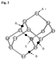
- FIG. 2 is a schematic diagram showing the structure of a C—O impurity complex in a silicon crystal, which is formed through a Czochralski crystal growth process.
- FIG. 3 is a schematic diagram showing the structure of a C—O impurity complex in a silicon crystal, which is experimentally determined through an extended x-ray absorption fine structure (EXAFS) spectroscopy.
- EXAFS extended x-ray absorption fine structure
- FIG. 4 is an explanatory diagram showing a process in which a deep impurity level (a) of a Cu impurity in a silicon crystal is vanished while splitting into a bonding state in the valence band and an antibonding state in the conduction band, in response to the formation of a Cu—O—C impurity complex, and changed into a Cu—O—C impurity level.
- FIG. 5 is a graph showing the temperature dependences of respective diffusion coefficients of Ni and Cu in a silicon crystal, after codoping a C atom and an O atom into the silicon crystal, and then thermally annealing the imparity-doped silicon crystal.
- the present invention is directed to a method for gettering a transition metal impurity in a silicon crystal, comprising codoping two kinds of impurities consisting of oxygen (O) and carbon (C), into silicon, and then thermally annealing the impurity-doped silicon.
- the codoping may be achieved by introducing oxygen or carbon into a silicon melt during the course of forming a silicon crystal through a Czochralski crystal pulling process to be performed in advance of the preparation of a silicon wafer. While oxygen is generally introduced from surrounding air naturally or in a natural manner, its concentration should be controlled. Thus, both oxygen (O) and carbon (C) are preferably codoped artificially or in an artificial manner while controlling the concentration thereof.
- the oxygen (O) and carbon (C) may be codoped into a silicon wafer in an artificial manner through an ion injection process.
- the codoped oxygen (O) and carbon (C) is set at a concentration equal to or greater than that of the transition metal impurity, for example, in the range of about 10 15 to 10 19 cm ⁇ 3 .
- a carbon (C) atom is doped in an artificial manner at a Si-substituting position in a silicon crystal, a strain field with long-range interactions will be formed because the carbon (C) atom has an atomic radius less than that of a silicon (Si) atom.
- the oxygen (O) doped into a silicon crystal in a natural manner or in an artificial manner through a Czochralski crystal growth process, or the oxygen (O) doped into a silicon crystal in an artificial manner through an ion injection process gets at an interstitial position of the silicon bond.
- the silicon crystal containing the two kinds of doped C and O is subjected to a thermal annealing treatment.
- the thermal annealing treatment is performed by placing a silicon wafer in an electric furnace, and heating under a nitrogen gas or argon gas atmosphere at a temperature of 250° C. or more, preferably at a temperature ranging from about 350 to 500° C. for about 10 minutes to 2 hours.
- a nitrogen gas or argon gas atmosphere As shown in FIG. 2 , through the thermal annealing treatment, O atoms getting at the interstitial position of the silicon bond are collected around a C atom at the Si-substituting position due to the strain field with long-range interactions arising from the C atom.
- the C atom is located at the central position of the interstitial bond.
- the strain field with long-range interactions in the C atom allows an atom of the transition metal impurity to be weakly drawn to the C atom, so as to form an impurity complex in combination with the O atoms collected around the C atom through the thermal annealing treatment, and precipitate the impurity complex consisting of the transition metal, the C atm and the O atoms, at a specific atomic position in the silicon crystal.
- the structure of the impurity complex containing the transition metal was experimentally determined through an EXAFS spectroscopy. As a result, it was proved that the impurity complex has a configuration as shown in FIG. 3 .
- the specific atomic position herein means an interstitial position which is located in the vicinity of the carbon (C), and allows the transition metal to be strongly bonded with the oxygen (O) so as to form a compound, as shown in FIG. 3 .
- the transition metal impurity is confined in the impurity complex.
- a deep impurity level is split into a bonding state (in the valence band) and an antibonding state (in the conduction band), and vanished.
- the deep impurity level can be electrically deactivated.
- FIG. 5 also shows the temperature dependences of respective diffusion coefficients of a Si atom in the silicon crystal and a p-donor impurity in the silicon crystal.
- the electrical activity and ultra high-speed diffusion of a transition metal impurity can be controlled by a simple thermal annealing treatment during the device production process.
- a simple thermal annealing treatment during the device production process.
- oxygen (O) and carbon (C) were codoped into a silicon melt.
- a low-resistance n-type silicon single crystal doped with the oxygen (O) and carbon (C) at a concentration of 8 ⁇ 10 18 cm ⁇ 3 which is equal to or greater than that of a copper impurity was obtained.
- a wafer obtained from this single crystal had an electrical resistivity of 1 ⁇ cm.
- Cu was doped into the above wafer at a concentration of 4 ⁇ 10 18 cm ⁇ 3 through an ion injection process. Then, the wafer was placed in an electric furnace, and thermally annealed under an argon atmosphere at each of temperatures of 100° C., 200° C., 300° C., 350° C., 400° C. and 500° C., for 16 minutes.
- the electrical resistivity of the wafer after the thermal annealing treatment was measured. As shown in Table 1, in case of the thermal annealing treatment at a temperature of 350° C. or more, the electrical resistivity of the wafer was not substantially changed from 1 ⁇ cm. A wafer subjected to no thermal annealing treatment (annealing temperature—in Table 1) has a resistivity of 8569 ⁇ cm. In view of these data, it was verified that deep impurity levels due to the doped Cu are vanished by the codoping of the oxygen and carbon and the thermal annealing treatment.
- the electrical activity and ultra high-speed diffusion in deep impurity levels of a transition metal impurity, such as Co, Ni or Cu, can be controlled by a simple treatment during a device production process.
- a transition metal impurity such as Co, Ni or Cu
- the present invention can contribute to provide high-performance silicon semiconductor devices.
Landscapes
- Chemical & Material Sciences (AREA)
- Engineering & Computer Science (AREA)
- Crystallography & Structural Chemistry (AREA)
- Materials Engineering (AREA)
- Metallurgy (AREA)
- Organic Chemistry (AREA)
- Crystals, And After-Treatments Of Crystals (AREA)
Abstract
Description
-
- Patent Publication 3: Japanese Patent Laid-Open Publication No. 2001-274405
| TABLE 1 | |
| annealing temperature | |
| — | 100 | 200 | 300 | 350 | 400 | 500 | |
| resistivity after | 8569 | 367 | 58.0 | 9.60 | 1.02 | 0.98 | 0.67 |
| annealing for 16 | |||||||
| minutes (Ωcm) | |||||||
Claims (3)
Applications Claiming Priority (3)
| Application Number | Priority Date | Filing Date | Title |
|---|---|---|---|
| JP2002003896A JP2003209114A (en) | 2002-01-10 | 2002-01-10 | Method for gettering transition metal impurities in silicon crystal |
| JP2002-003896 | 2002-10-01 | ||
| PCT/JP2003/000139 WO2003060981A1 (en) | 2002-01-10 | 2003-01-09 | Method for gettering transition metal impurities in silicon crystal |
Publications (2)
| Publication Number | Publication Date |
|---|---|
| US20050090079A1 US20050090079A1 (en) | 2005-04-28 |
| US7157354B2 true US7157354B2 (en) | 2007-01-02 |
Family
ID=19190931
Family Applications (1)
| Application Number | Title | Priority Date | Filing Date |
|---|---|---|---|
| US10/501,080 Expired - Fee Related US7157354B2 (en) | 2002-01-10 | 2003-01-09 | Method for gettering transition metal impurities in silicon crystal |
Country Status (6)
| Country | Link |
|---|---|
| US (1) | US7157354B2 (en) |
| EP (1) | EP1467405A1 (en) |
| JP (1) | JP2003209114A (en) |
| KR (1) | KR100596701B1 (en) |
| TW (1) | TWI232897B (en) |
| WO (1) | WO2003060981A1 (en) |
Families Citing this family (7)
| Publication number | Priority date | Publication date | Assignee | Title |
|---|---|---|---|---|
| JP4684574B2 (en) * | 2004-04-30 | 2011-05-18 | 独立行政法人科学技術振興機構 | Method for gettering Cu impurity in silicon crystal |
| JP4604889B2 (en) * | 2005-05-25 | 2011-01-05 | 株式会社Sumco | Silicon wafer manufacturing method and silicon single crystal growing method |
| JP2007220825A (en) | 2006-02-15 | 2007-08-30 | Sumco Corp | Silicon wafer manufacturing method |
| JP2010016169A (en) * | 2008-07-03 | 2010-01-21 | Shin Etsu Handotai Co Ltd | Epitaxial wafer and method for manufacturing epitaxial wafer |
| CN105140355A (en) * | 2015-08-18 | 2015-12-09 | 西安电子科技大学 | M-surface sapphire substrate based semi-polar (11-22) yellow light-emitting diode (LED) material and fabrication method thereof |
| CN105140365B (en) * | 2015-08-18 | 2018-03-06 | 西安电子科技大学 | Based on Ga polarity gold-tinted LED structure and preparation method thereof in c surface sapphire substrates |
| CN105098017B (en) * | 2015-08-18 | 2018-03-06 | 西安电子科技大学 | Based on N faces yellow light LED structure and preparation method thereof in c surface sapphire substrates |
Citations (6)
| Publication number | Priority date | Publication date | Assignee | Title |
|---|---|---|---|---|
| EP0419044A1 (en) | 1989-08-23 | 1991-03-27 | Shin-Etsu Handotai Company, Limited | Single crystal silicon |
| EP0502471A2 (en) | 1991-03-05 | 1992-09-09 | Fujitsu Limited | Intrinsic gettering of a silicon substrate |
| JPH1041311A (en) | 1996-07-18 | 1998-02-13 | Sony Corp | Epitaxial silicon substrate, solid-state imaging device, and manufacturing method thereof |
| JPH11204534A (en) | 1998-01-14 | 1999-07-30 | Sumitomo Metal Ind Ltd | Method for manufacturing silicon epitaxial wafer |
| US20010012686A1 (en) | 2000-02-04 | 2001-08-09 | Nec Corporation, | Semiconductor device and fabricating method thereof |
| US6277501B1 (en) | 1996-07-29 | 2001-08-21 | Sumitomo Metal Industries, Ltd. | Silicon epitaxial wafer and method for manufacturing the same |
-
2002
- 2002-01-10 JP JP2002003896A patent/JP2003209114A/en active Pending
-
2003
- 2003-01-09 US US10/501,080 patent/US7157354B2/en not_active Expired - Fee Related
- 2003-01-09 EP EP03701051A patent/EP1467405A1/en not_active Withdrawn
- 2003-01-09 TW TW092100378A patent/TWI232897B/en not_active IP Right Cessation
- 2003-01-09 KR KR1020047010635A patent/KR100596701B1/en not_active Expired - Fee Related
- 2003-01-09 WO PCT/JP2003/000139 patent/WO2003060981A1/en not_active Ceased
Patent Citations (6)
| Publication number | Priority date | Publication date | Assignee | Title |
|---|---|---|---|---|
| EP0419044A1 (en) | 1989-08-23 | 1991-03-27 | Shin-Etsu Handotai Company, Limited | Single crystal silicon |
| EP0502471A2 (en) | 1991-03-05 | 1992-09-09 | Fujitsu Limited | Intrinsic gettering of a silicon substrate |
| JPH1041311A (en) | 1996-07-18 | 1998-02-13 | Sony Corp | Epitaxial silicon substrate, solid-state imaging device, and manufacturing method thereof |
| US6277501B1 (en) | 1996-07-29 | 2001-08-21 | Sumitomo Metal Industries, Ltd. | Silicon epitaxial wafer and method for manufacturing the same |
| JPH11204534A (en) | 1998-01-14 | 1999-07-30 | Sumitomo Metal Ind Ltd | Method for manufacturing silicon epitaxial wafer |
| US20010012686A1 (en) | 2000-02-04 | 2001-08-09 | Nec Corporation, | Semiconductor device and fabricating method thereof |
Non-Patent Citations (6)
| Title |
|---|
| C. Maddalon-Vinante et al.; Journal of the Electrochemical Society, vol. 142, No. 2, pp. 560-564, Feb. 1995. Cited in the int'l. search report. |
| M. Nakamura, Applied Physics Letters, vol. 79, No. 18, pp. 2904-2906; Oct. 29, 2001. |
| M. Nakamura, Journal of the Electrochemical Society, vol. 147, No. 2, pp. 796-798, 2000. |
| Patent Abstracts of Japan, Pub. No. 10-303430 of Nov. 13, 1998. Cited in the specification. |
| Patent Abstracts of Japan, Pub. No. 2001-250957 of Sep. 14, 2001. Cited in the spec. |
| Patent Abstracts of Japan, Pub. No. 2001-274405 of Oct. 5, 2001. Cited in the spec. |
Also Published As
| Publication number | Publication date |
|---|---|
| WO2003060981A1 (en) | 2003-07-24 |
| EP1467405A1 (en) | 2004-10-13 |
| TWI232897B (en) | 2005-05-21 |
| TW200301786A (en) | 2003-07-16 |
| KR20040076882A (en) | 2004-09-03 |
| US20050090079A1 (en) | 2005-04-28 |
| JP2003209114A (en) | 2003-07-25 |
| KR100596701B1 (en) | 2006-07-04 |
Similar Documents
| Publication | Publication Date | Title |
|---|---|---|
| JP3288721B2 (en) | Ideal oxygen-precipitated silicon wafers and oxygen-free diffusion-free method therefor | |
| US7846252B2 (en) | Silicon wafer for IGBT and method for producing same | |
| JP3711199B2 (en) | Heat treatment method for silicon substrate | |
| KR100816696B1 (en) | Opened wafer with improved internal gettering | |
| EP2037009A2 (en) | Method for producing a bonded SOI wafer | |
| US6551398B2 (en) | Heat treatment method for a silicon monocrystal wafer and a silicon monocrystal wafer | |
| JP2002532875A (en) | Epitaxial silicon wafer having internal gettering and method of manufacturing the same | |
| EP0915502B1 (en) | Method for heat treatment of silicon wafer and silicon wafer heat-treated by the method | |
| KR20010082183A (en) | Process for preparing an ideal oxygen precipitating silicon wafer | |
| EP0917188B1 (en) | Method for heat treatment of SOI wafer and SOI wafer heat-treated by the method | |
| EP2607526B1 (en) | Method of manufacturing a silicon single crystal substrate | |
| JP2002043318A (en) | Method for manufacturing silicon single crystal wafer | |
| US7157354B2 (en) | Method for gettering transition metal impurities in silicon crystal | |
| Perichaud et al. | Multicrystalline silicon prepared by electromagnetic continuous pulling: recent results and comparison to directional solidification material | |
| KR100625822B1 (en) | Silicon wafer and process for producing it | |
| EP0973190A2 (en) | Silicon wafer and method for producing it | |
| EP1298731B1 (en) | Simox substrate production process | |
| JP2000269221A (en) | Heat treatment method for silicon substrate, heat-treated substrate, and epitaxial wafer using the substrate | |
| EP1879224A2 (en) | Process for controlling denuded zone depth in an ideal oxygen precipitating silicon wafer | |
| JPH07126094A (en) | Silicon single crystal manufacturing equipment | |
| JP4684574B2 (en) | Method for gettering Cu impurity in silicon crystal | |
| JP2017157812A (en) | Wafer heat treatment method | |
| JPS61137332A (en) | Manufacture of high speed semiconductor device | |
| JPH06102598B2 (en) | Method for manufacturing semiconductor device material | |
| JPH04287328A (en) | Gettering processing |
Legal Events
| Date | Code | Title | Description |
|---|---|---|---|
| AS | Assignment |
Owner name: JAPAN SCIENCE AND TECHNOLOGY AGENCY, JAPAN Free format text: ASSIGNMENT OF ASSIGNORS INTEREST;ASSIGNOR:YOSHIDA, HIROSHI;REEL/FRAME:016075/0468 Effective date: 20040820 |
|
| AS | Assignment |
Owner name: JAPAN SCIENCE AND TECHNOLOGY AGENCY, JAPAN Free format text: ASSIGNMENT OF ASSIGNORS INTEREST;ASSIGNOR:YOSHIDA, HIROSHI;REEL/FRAME:016764/0645 Effective date: 20040820 |
|
| FEPP | Fee payment procedure |
Free format text: PAYOR NUMBER ASSIGNED (ORIGINAL EVENT CODE: ASPN); ENTITY STATUS OF PATENT OWNER: LARGE ENTITY |
|
| FPAY | Fee payment |
Year of fee payment: 4 |
|
| FEPP | Fee payment procedure |
Free format text: PAYER NUMBER DE-ASSIGNED (ORIGINAL EVENT CODE: RMPN); ENTITY STATUS OF PATENT OWNER: LARGE ENTITY Free format text: PAYOR NUMBER ASSIGNED (ORIGINAL EVENT CODE: ASPN); ENTITY STATUS OF PATENT OWNER: LARGE ENTITY |
|
| REMI | Maintenance fee reminder mailed | ||
| FEPP | Fee payment procedure |
Free format text: PAYER NUMBER DE-ASSIGNED (ORIGINAL EVENT CODE: RMPN); ENTITY STATUS OF PATENT OWNER: LARGE ENTITY Free format text: PAYOR NUMBER ASSIGNED (ORIGINAL EVENT CODE: ASPN); ENTITY STATUS OF PATENT OWNER: LARGE ENTITY |
|
| LAPS | Lapse for failure to pay maintenance fees | ||
| STCH | Information on status: patent discontinuation |
Free format text: PATENT EXPIRED DUE TO NONPAYMENT OF MAINTENANCE FEES UNDER 37 CFR 1.362 |
|
| STCH | Information on status: patent discontinuation |
Free format text: PATENT EXPIRED DUE TO NONPAYMENT OF MAINTENANCE FEES UNDER 37 CFR 1.362 |
|
| FP | Lapsed due to failure to pay maintenance fee |
Effective date: 20150102 |