US7109084B2 - Flash memory device and method for fabricating the same - Google Patents
Flash memory device and method for fabricating the same Download PDFInfo
- Publication number
- US7109084B2 US7109084B2 US11/121,495 US12149505A US7109084B2 US 7109084 B2 US7109084 B2 US 7109084B2 US 12149505 A US12149505 A US 12149505A US 7109084 B2 US7109084 B2 US 7109084B2
- Authority
- US
- United States
- Prior art keywords
- layer
- semiconductor substrate
- forming
- contact hole
- drain
- Prior art date
- Legal status (The legal status is an assumption and is not a legal conclusion. Google has not performed a legal analysis and makes no representation as to the accuracy of the status listed.)
- Expired - Fee Related
Links
Images


Classifications
-
- H—ELECTRICITY
- H10—SEMICONDUCTOR DEVICES; ELECTRIC SOLID-STATE DEVICES NOT OTHERWISE PROVIDED FOR
- H10B—ELECTRONIC MEMORY DEVICES
- H10B43/00—EEPROM devices comprising charge-trapping gate insulators
- H10B43/30—EEPROM devices comprising charge-trapping gate insulators characterised by the memory core region
-
- H—ELECTRICITY
- H10—SEMICONDUCTOR DEVICES; ELECTRIC SOLID-STATE DEVICES NOT OTHERWISE PROVIDED FOR
- H10B—ELECTRONIC MEMORY DEVICES
- H10B69/00—Erasable-and-programmable ROM [EPROM] devices not provided for in groups H10B41/00 - H10B63/00, e.g. ultraviolet erasable-and-programmable ROM [UVEPROM] devices
-
- H—ELECTRICITY
- H10—SEMICONDUCTOR DEVICES; ELECTRIC SOLID-STATE DEVICES NOT OTHERWISE PROVIDED FOR
- H10D—INORGANIC ELECTRIC SEMICONDUCTOR DEVICES
- H10D30/00—Field-effect transistors [FET]
- H10D30/60—Insulated-gate field-effect transistors [IGFET]
- H10D30/69—IGFETs having charge trapping gate insulators, e.g. MNOS transistors
-
- Y—GENERAL TAGGING OF NEW TECHNOLOGICAL DEVELOPMENTS; GENERAL TAGGING OF CROSS-SECTIONAL TECHNOLOGIES SPANNING OVER SEVERAL SECTIONS OF THE IPC; TECHNICAL SUBJECTS COVERED BY FORMER USPC CROSS-REFERENCE ART COLLECTIONS [XRACs] AND DIGESTS
- Y10—TECHNICAL SUBJECTS COVERED BY FORMER USPC
- Y10S—TECHNICAL SUBJECTS COVERED BY FORMER USPC CROSS-REFERENCE ART COLLECTIONS [XRACs] AND DIGESTS
- Y10S438/00—Semiconductor device manufacturing: process
- Y10S438/954—Making oxide-nitride-oxide device
Definitions
- the present invention relates to a flash memory device and a method for fabricating the same, and more particularly, to a flash memory device and a method for fabricating the same, which is suitable for improving integration in a SONOS (Silicon-Oxide-Nitride-Oxide-Silicon) cell.
- SONOS Silicon-Oxide-Nitride-Oxide-Silicon
- EEPROM Electrically Erasable Programmable Read Only Memory
- EEPROM devices use a floating gate type cell.
- the size of the floating gate type cell has generally decreased according to the related art.
- various nonvolatile memory devices such as SONOS, FeRAM, SET and NROM have been studied actively as a substitute for the floating gate type cell.
- SONOS cell has attracted great attention as a nonvolatile memory device that can substitute for the floating gate type cell.
- FIG. 1 is a layout of showing a unit cell of an SONOS type nonvolatile memory device according to the related art.
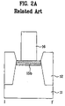
- FIG. 2A is a cross sectional view along I–I′ of FIG. 1 .
- FIG. 2B is a cross sectional view along II–II′ of FIG. 1 .
- FIG. 2C is a cross sectional view of showing a pattern defect due to misalignment.
- the unit cell of the SONOS type nonvolatile memory device includes a semiconductor substrate 11 , a device isolation layer 12 , an ONO layer 13 , and a gate electrode 14 .
- the device isolation layer 12 an STI, or Shallow Trench Isolation, structure
- the semiconductor substrate 11 is formed in the semiconductor substrate 11 , to divide the semiconductor substrate 11 into a field region and an active region.
- the ONO layer 13 is formed by sequentially stacking a lower oxide layer 13 a , a nitride layer 13 b and an upper oxide layer 13 c in order, wherein the lower oxide layer 13 a is used as a tunnel oxide layer, the nitride layer 13 b functions as a memory (storage) layer, and the upper oxide layer 13 c functions as a gate dielectric or blocking layer for preventing the loss of electric charges.
- the gate electrode 14 is formed on the ONO layer 13 .
- source and drain regions 15 a and 15 b are formed at both sides of the gate electrode 14 in the active region of the semiconductor substrate 11 .
- a drain contact hole 16 is formed in the drain region 15 b , for connection with an upper line.
- the device isolation layer 12 is formed of an insulating layer in an STI (Shallow Trench Isolation) process. Recently, as dimensions in design rules for high integration semiconductor device decrease, the distance between the device isolation layers 12 becomes small. Accordingly, when the drain region 15 b is formed in the semiconductor substrate 11 between the device isolation layers 12 , a width of the drain region 15 b is also decreased, so that it is difficult to obtain a sufficient interval between the drain contact hole 16 and the device isolation layer 12 .
- STI Shallow Trench Isolation
- the drain contact hole 16 may be formed above the device isolation layer 12 as well as above the drain region 15 b . That is, when forming the drain contact hole 16 , a portion of the semiconductor substrate 11 adjacent to the device isolation layer 12 may be etched, thereby generating junction leakage. Accordingly, the memory device may operate incorrectly or fail.
- the present invention is directed to a flash memory device and a method for fabricating the same that substantially obviates one or more problems due to limitations and disadvantages of the related art.
- An object of the present invention is to provide a flash memory device and a method for fabricating the same, in which it is possible to prevent mis-operation by reducing or preventing junction leakage in a drain contact hole, and to improve integration by decreasing a unit cell size in an SONOS type nonvolatile memory device.
- a flash memory device includes a semiconductor substrate having a field region and an active region; a device isolation layer on the field region of the semiconductor substrate, wherein the device isolation layer comprises a conductive (e.g., polysilicon) layer with an insulating layer thereon; an insulating sidewall spacer at a side of the device isolation layer; an ONO layer on the active region of the semiconductor substrate; a gate electrode on the ONO layer; source and drain regions at sides of the gate electrode in the active region of the semiconductor substrate; a passivation layer on the semiconductor substrate, having a contact hole in the drain region; and a drain electrode in the contact hole, connected to the drain region.
- a conductive e.g., polysilicon
- a method for fabricating a flash memory device includes the steps of forming a device isolating layer having a first insulating layer, a conductive (e.g., polysilicon) layer and a second insulating layer on a field region of a semiconductor substrate; forming an insulating sidewall spacer at a side of the device isolation layer; forming an ONO layer on an active region of the semiconductor substrate, and forming a gate electrode on the ONO layer; forming source and drain regions by implanting impurity ions into the active region of the semiconductor substrate using the gate electrode as a mask; forming a passivation layer on an entire surface of the semiconductor substrate; and forming a contact hole in the passivation layer over the drain region.
- a device isolating layer having a first insulating layer, a conductive (e.g., polysilicon) layer and a second insulating layer on a field region of a semiconductor substrate
- FIG. 1 is a layout of showing a unit cell of an SONOS type nonvolatile memory device according to the related art
- FIG. 2A is a cross sectional view along I–I′ of FIG. 1 ;
- FIG. 2B is a cross sectional view along II–II′ of FIG. 1 ;
- FIG. 2C is a cross sectional view of showing a pattern defect generated due to misalignment
- FIG. 3 is a layout of showing a unit cell of an SONOS type nonvolatile memory device according to the present invention
- FIG. 4A is a cross sectional view along III–III′ of FIG. 3 ;
- FIG. 4B is a cross sectional view along IV–IV′ of FIG. 3 ;
- FIG. 5A and FIG. 5B are cross sectional views of showing the process for fabricating a unit cell of an SONOS type nonvolatile memory device, along IV–IV′ of FIG. 3 , according to the present invention.
- FIG. 3 is a layout of showing a unit cell of an SONOS type nonvolatile memory device according to the present invention.
- FIG. 4A is a cross sectional view along III–III′ of FIG. 3 .
- FIG. 4B is a cross sectional view along IV–IV′ of FIG. 3 .
- the unit cell of the SONOS type nonvolatile memory device there are a semiconductor substrate 31 , a device isolation layer 32 , insulating sidewall spacers 33 , an ONO layer 34 , a gate electrode 35 , source and drain regions 36 a and 36 b , a passivation layer 38 , and a drain electrode 37 .
- the device isolation layer 32 divides the semiconductor substrate 31 into an active region and a field region.
- the device isolation layer 32 is in the field region of the semiconductor substrate 31 .
- the outer borders of device isolation layer 32 define the field region.
- the device isolation layer 32 is formed by sequentially stacking an oxide layer 32 a , a conductive (e.g., polysilicon) layer 32 b , an oxide layer 32 c and a nitride layer 32 d in order. Also, the insulating sidewall spacers 33 are formed at the side of the device isolation layer 32 . Then, the ONO layer 34 is formed across the active region of the semiconductor substrate 31 .
- the ONO layer 34 comprises a lower oxide layer 34 a , a nitride layer 34 b and an upper oxide layer 34 c .
- the lower oxide layer 34 a generally functions as a tunnel oxide layer
- the nitride layer 34 b functions as a memory (storage) layer
- the upper oxide layer 34 c functions as a blocking layer for preventing the loss of electric charges.
- the gate electrode 35 is formed on the ONO layer 34 .
- the gate electrode 35 generally comprises a polysilicon layer (which may be [heavily] doped and/or which may further comprise a metal silicide layer thereon) that may be covered with an insulating layer (not shown).
- the source and drain regions 36 a and 36 b are formed at both sides of the ONO layer 34 and the gate electrode 35 in the active region of the semiconductor substrate 31 .
- a passivation layer 38 is formed on an entire surface of the semiconductor substrate 31 including the gate electrode 35 , and a contact hole is formed in the passivation layer 38 to expose a predetermine portion of the drain region 36 b . Accordingly, the drain electrode 37 in the contact hole is connected to the drain region 36 b . In this case, the contact hole for connection of the drain electrode 37 in the device isolation layer 32 is self aligned to the insulating sidewall spacers 33 above the drain region 36 b . Thus, the contact hole exposes the drain region 36 b of the semiconductor substrate 31 and part of the insulating sidewall spacer(s) 33 .
- conductive layer 32 b generally comprises polysilicon (which, like gate electrode 35 , may be [heavily] doped and/or which may further comprise a metal silicide layer thereon), other conductors, such as aluminum, titanium, titanium nitride, tungsten, metal alloys thereof or other metals or conductive metal compounds may be employed. Also, when conductive layer 32 b generally comprises polysilicon, although not shown, an oxide layer may be formed at the side of the polysilicon layer 32 b . Furthermore, the conductive layer 32 b may be connected with a ground terminal, which generally has the same structure as a ground gate in a general MOS transistor or ground plane in a general MOS integrated circuit.
- the contact hole is self-aligned to the insulating sidewall spacers 33 . As a result, it is not necessary to obtain or provide an interval or distance between the contact hole and the device isolation layer 32 . Also, as shown in FIG. 4A , the contact hole may expose part of the insulating sidewall spacer(s) 33 over the drain region 36 b.
- a method for fabricating the aforementioned unit cell of the SONOS type nonvolatile memory device according to the present invention will be described as follows.
- FIG. 5A and FIG. 5B are cross sectional views of showing the process for fabricating the unit cell of the SONOS type nonvolatile memory device, along IV–IV of FIG. 3 , according to the present invention.
- the oxide layer 32 a , the conductive (e.g., polysilicon) layer 32 b , the oxide layer 32 c and the nitride layer 32 d are sequentially stacked on the semiconductor substrate 31 , the semiconductor substrate 31 having an active region and a field region. Then, portions of the oxide layer 32 a , the polysilicon layer 32 b , the oxide layer 32 c and the nitride layer 32 d that are over the active region of the semiconductor substrate 31 are selectively removed, thereby forming the device isolation layer 32 .
- a well is formed by a doping process (e.g., ion implantation).
- a doping process e.g., ion implantation.
- the polysilicon layer 32 b of the device isolation layer 32 may be oxidized, so that an oxide layer (not shown) may be formed at the side of the polysilicon layer 32 b.
- a spacer insulating material e.g., a nitride layer
- a spacer insulating material is formed on the entire surface of the semiconductor substrate 31 and then anisotropically etched, thereby forming the insulating sidewall spacers 33 at sides of the device isolation layer 32 .
- the ONO layer 34 is formed on the entire surface of the semiconductor substrate 31 .
- the ONO layer 34 generally comprises a lower oxide layer 34 a , a nitride layer 34 b and an upper oxide layer 34 c .
- the lower oxide layer 34 a functions as a tunnel oxide layer
- the nitride layer 34 b functions as the memory (storage) layer
- the upper oxide layer 34 c functions as the blocking layer for preventing the loss of electric charges.
- a gate material layer e.g., comprising polysilicon, which may be [heavily] doped and/or silicided
- the gate electrode 35 may be oxidized before forming the source and drain regions.
- the passivation layer 38 is formed on the entire surface of the semiconductor substrate 31 including the gate electrode 35 and the source and drain regions 36 a and 36 b , and a portion of the passivation layer 38 is selectively removed above the drain region 36 b to form the contact hole.
- the contact hole is formed in the device isolation layer 32 self aligned to the insulating layer sidewall spacers 33 .
- a conductive material is deposited on the entire surface of the semiconductor substrate 31 , and then is selectively removed, whereby the drain electrode 37 is electrically connected with the drain region 36 b in the contact hole.
- the polysilicon layer 32 b of the device isolation layer 32 may be connected with a ground terminal.
- the flash memory device and the method for fabricating the same according to the present invention has the following advantages.
- the contact hole for connection of the drain electrode is formed in the device isolation layer by self alignment. That is, when forming the contact hole, a predetermined portion of the device isolation layer is etched, exposing only the drain region 36 b of the semiconductor substrate therebelow, thereby reducing or preventing the junction leakage. Accordingly, it is possible to minimize or prevent mis-operation in the flash memory device.
Landscapes
- Non-Volatile Memory (AREA)
- Semiconductor Memories (AREA)
Abstract
Description
Claims (9)
Applications Claiming Priority (2)
| Application Number | Priority Date | Filing Date | Title |
|---|---|---|---|
| KR1020040031863A KR100546693B1 (en) | 2004-05-06 | 2004-05-06 | Flash memory device and manufacturing method thereof |
| KR10-2004-0031863 | 2004-05-06 |
Publications (2)
| Publication Number | Publication Date |
|---|---|
| US20050247987A1 US20050247987A1 (en) | 2005-11-10 |
| US7109084B2 true US7109084B2 (en) | 2006-09-19 |
Family
ID=35238685
Family Applications (1)
| Application Number | Title | Priority Date | Filing Date |
|---|---|---|---|
| US11/121,495 Expired - Fee Related US7109084B2 (en) | 2004-05-06 | 2005-05-03 | Flash memory device and method for fabricating the same |
Country Status (3)
| Country | Link |
|---|---|
| US (1) | US7109084B2 (en) |
| JP (1) | JP2005322927A (en) |
| KR (1) | KR100546693B1 (en) |
Cited By (1)
| Publication number | Priority date | Publication date | Assignee | Title |
|---|---|---|---|---|
| US20090014779A1 (en) * | 2007-07-11 | 2009-01-15 | Koichi Kawashima | Nonvolatile semiconductor memory device and method for fabricating the same |
Families Citing this family (1)
| Publication number | Priority date | Publication date | Assignee | Title |
|---|---|---|---|---|
| KR100824535B1 (en) * | 2006-11-20 | 2008-04-24 | 동부일렉트로닉스 주식회사 | Flash memory cell and manufacturing method thereof |
Citations (3)
| Publication number | Priority date | Publication date | Assignee | Title |
|---|---|---|---|---|
| US5436481A (en) * | 1993-01-21 | 1995-07-25 | Nippon Steel Corporation | MOS-type semiconductor device and method of making the same |
| US6881619B1 (en) * | 2003-12-23 | 2005-04-19 | Macronix International Co. | Method for fabricating a non-volatile memory and metal interconnect process |
| US7018896B2 (en) * | 2003-02-05 | 2006-03-28 | Advanced Micro Devices, Inc. | UV-blocking layer for reducing UV-induced charging of SONOS dual-bit flash memory devices in BEOL processing |
-
2004
- 2004-05-06 KR KR1020040031863A patent/KR100546693B1/en not_active Expired - Fee Related
-
2005
- 2005-05-03 US US11/121,495 patent/US7109084B2/en not_active Expired - Fee Related
- 2005-05-06 JP JP2005135136A patent/JP2005322927A/en active Pending
Patent Citations (3)
| Publication number | Priority date | Publication date | Assignee | Title |
|---|---|---|---|---|
| US5436481A (en) * | 1993-01-21 | 1995-07-25 | Nippon Steel Corporation | MOS-type semiconductor device and method of making the same |
| US7018896B2 (en) * | 2003-02-05 | 2006-03-28 | Advanced Micro Devices, Inc. | UV-blocking layer for reducing UV-induced charging of SONOS dual-bit flash memory devices in BEOL processing |
| US6881619B1 (en) * | 2003-12-23 | 2005-04-19 | Macronix International Co. | Method for fabricating a non-volatile memory and metal interconnect process |
Cited By (2)
| Publication number | Priority date | Publication date | Assignee | Title |
|---|---|---|---|---|
| US20090014779A1 (en) * | 2007-07-11 | 2009-01-15 | Koichi Kawashima | Nonvolatile semiconductor memory device and method for fabricating the same |
| US7791121B2 (en) * | 2007-07-11 | 2010-09-07 | Panasonic Corporation | Nonvolatile semiconductor memory device and method for fabricating the same |
Also Published As
| Publication number | Publication date |
|---|---|
| JP2005322927A (en) | 2005-11-17 |
| US20050247987A1 (en) | 2005-11-10 |
| KR100546693B1 (en) | 2006-01-26 |
| KR20050106820A (en) | 2005-11-11 |
Similar Documents
| Publication | Publication Date | Title |
|---|---|---|
| US7767522B2 (en) | Semiconductor device and a method of manufacturing the same | |
| KR100398955B1 (en) | Eeprom memory cell and method of forming the same | |
| US6197639B1 (en) | Method for manufacturing NOR-type flash memory device | |
| US6900086B2 (en) | Semiconductor device having MISFETs | |
| US6797570B2 (en) | NAND-type flash memory devices and methods of fabricating the same | |
| US6750525B2 (en) | Non-volatile memory device having a metal-oxide-nitride-oxide-semiconductor gate structure | |
| US7588983B2 (en) | EEPROM cell and EEPROM device with high integration and low source resistance and method of manufacturing the same | |
| US7094652B2 (en) | Semiconductor device and method of manufacturing the same | |
| US20040238847A1 (en) | Semiconductor device and manufacturing method | |
| US20060214254A1 (en) | Semiconductor device and manufacturing method of the same | |
| US9905429B2 (en) | Semiconductor device and a manufacturing method thereof | |
| US8952536B2 (en) | Semiconductor device and method of fabrication | |
| US8043912B2 (en) | Manufacturing method of a semiconductor device having polycide wiring layer | |
| US6451653B2 (en) | Manufacturing process for the integration in a semiconductor chip of an integrated circuit including a high-density integrated circuit components portion and a high-performance logic integrated circuit components portion | |
| US8207560B2 (en) | Nonvolatile semiconductor memory device and method of fabricating the same | |
| KR100275735B1 (en) | Method for manufacturing nor-type flash memory device | |
| US7626227B2 (en) | Semiconductor device with reduced transistor breakdown voltage for preventing substrate junction currents | |
| US7041555B2 (en) | Method for manufacturing flash memory device | |
| US7109084B2 (en) | Flash memory device and method for fabricating the same | |
| JP2002231832A (en) | Nonvolatile semiconductor memory device and method of manufacturing the same | |
| US20010004330A1 (en) | Non-volatile semiconductor memory device and manufacturing method thereof | |
| US20080197402A1 (en) | Methods of Forming Nonvolatile Memory Devices and Memory Devices Formed Thereby | |
| EP0962982A1 (en) | Byte-switch structure for EEPROM memories | |
| JPH09181282A (en) | Nonvolatile semiconductor memory device and method of manufacturing the same |
Legal Events
| Date | Code | Title | Description |
|---|---|---|---|
| AS | Assignment |
Owner name: DONGBUANAM SEMICONDUCTOR, INC., KOREA, REPUBLIC OF Free format text: ASSIGNMENT OF ASSIGNORS INTEREST;ASSIGNOR:LEE, SANG BUM;REEL/FRAME:016535/0323 Effective date: 20050503 |
|
| AS | Assignment |
Owner name: DONGBU ELECTRONICS CO., LTD.,KOREA, REPUBLIC OF Free format text: CHANGE OF NAME;ASSIGNOR:DONGANAM SEMICONDUCTOR INC.;REEL/FRAME:017654/0078 Effective date: 20060328 Owner name: DONGBU ELECTRONICS CO., LTD., KOREA, REPUBLIC OF Free format text: CHANGE OF NAME;ASSIGNOR:DONGANAM SEMICONDUCTOR INC.;REEL/FRAME:017654/0078 Effective date: 20060328 |
|
| AS | Assignment |
Owner name: DONGBU ELECTRONICS CO., LTD., KOREA, REPUBLIC OF Free format text: CORRECTIVE ASSIGNMENT TO CORRECT THE ASSIGNOR PREVIOUSLY RECORDED ON REEL 017654 FRAME 0078;ASSIGNOR:DONGBUANAM SEMICONDUCTOR INC.;REEL/FRAME:017829/0911 Effective date: 20060328 Owner name: DONGBU ELECTRONICS CO., LTD.,KOREA, REPUBLIC OF Free format text: CORRECTIVE ASSIGNMENT TO CORRECT THE ASSIGNOR PREVIOUSLY RECORDED ON REEL 017654 FRAME 0078. ASSIGNOR(S) HEREBY CONFIRMS THE ASSIGNOR SHOULD BE "DONGBUANAM SEMICONDUCTOR INC.";ASSIGNOR:DONGBUANAM SEMICONDUCTOR INC.;REEL/FRAME:017829/0911 Effective date: 20060328 Owner name: DONGBU ELECTRONICS CO., LTD., KOREA, REPUBLIC OF Free format text: CORRECTIVE ASSIGNMENT TO CORRECT THE ASSIGNOR PREVIOUSLY RECORDED ON REEL 017654 FRAME 0078. ASSIGNOR(S) HEREBY CONFIRMS THE ASSIGNOR SHOULD BE "DONGBUANAM SEMICONDUCTOR INC.";ASSIGNOR:DONGBUANAM SEMICONDUCTOR INC.;REEL/FRAME:017829/0911 Effective date: 20060328 |
|
| FEPP | Fee payment procedure |
Free format text: PAYOR NUMBER ASSIGNED (ORIGINAL EVENT CODE: ASPN); ENTITY STATUS OF PATENT OWNER: LARGE ENTITY |
|
| FEPP | Fee payment procedure |
Free format text: PAYER NUMBER DE-ASSIGNED (ORIGINAL EVENT CODE: RMPN); ENTITY STATUS OF PATENT OWNER: LARGE ENTITY Free format text: PAYOR NUMBER ASSIGNED (ORIGINAL EVENT CODE: ASPN); ENTITY STATUS OF PATENT OWNER: LARGE ENTITY |
|
| FPAY | Fee payment |
Year of fee payment: 4 |
|
| REMI | Maintenance fee reminder mailed | ||
| AS | Assignment |
Owner name: DSS TECHNOLOGY MANAGEMENT, INC., VIRGINIA Free format text: ASSIGNMENT OF ASSIGNORS INTEREST;ASSIGNOR:DONGBU HITEK CO., LTD.;REEL/FRAME:033035/0680 Effective date: 20140522 |
|
| LAPS | Lapse for failure to pay maintenance fees | ||
| STCH | Information on status: patent discontinuation |
Free format text: PATENT EXPIRED DUE TO NONPAYMENT OF MAINTENANCE FEES UNDER 37 CFR 1.362 |
|
| STCH | Information on status: patent discontinuation |
Free format text: PATENT EXPIRED DUE TO NONPAYMENT OF MAINTENANCE FEES UNDER 37 CFR 1.362 |
|
| FP | Lapsed due to failure to pay maintenance fee |
Effective date: 20140919 |