US7101754B2 - Titanium silicate films with high dielectric constant - Google Patents
Titanium silicate films with high dielectric constant Download PDFInfo
- Publication number
- US7101754B2 US7101754B2 US10/864,472 US86447204A US7101754B2 US 7101754 B2 US7101754 B2 US 7101754B2 US 86447204 A US86447204 A US 86447204A US 7101754 B2 US7101754 B2 US 7101754B2
- Authority
- US
- United States
- Prior art keywords
- film
- sol
- gel
- dielectric constant
- titanium silicate
- Prior art date
- Legal status (The legal status is an assumption and is not a legal conclusion. Google has not performed a legal analysis and makes no representation as to the accuracy of the status listed.)
- Expired - Lifetime
Links
- GNKTZDSRQHMHLZ-UHFFFAOYSA-N [Si].[Si].[Si].[Ti].[Ti].[Ti].[Ti].[Ti] Chemical compound [Si].[Si].[Si].[Ti].[Ti].[Ti].[Ti].[Ti] GNKTZDSRQHMHLZ-UHFFFAOYSA-N 0.000 title claims description 38
- VYPSYNLAJGMNEJ-UHFFFAOYSA-N Silicium dioxide Chemical compound O=[Si]=O VYPSYNLAJGMNEJ-UHFFFAOYSA-N 0.000 claims abstract description 137
- GWEVSGVZZGPLCZ-UHFFFAOYSA-N Titan oxide Chemical compound O=[Ti]=O GWEVSGVZZGPLCZ-UHFFFAOYSA-N 0.000 claims abstract description 104
- 239000000377 silicon dioxide Substances 0.000 claims abstract description 69
- 229910052681 coesite Inorganic materials 0.000 claims abstract description 67
- 229910052906 cristobalite Inorganic materials 0.000 claims abstract description 67
- 229910052682 stishovite Inorganic materials 0.000 claims abstract description 67
- 229910052905 tridymite Inorganic materials 0.000 claims abstract description 67
- 239000000203 mixture Substances 0.000 claims abstract description 18
- 238000003980 solgel method Methods 0.000 claims abstract description 14
- 239000000758 substrate Substances 0.000 claims abstract description 12
- 239000012298 atmosphere Substances 0.000 claims abstract description 10
- QVGXLLKOCUKJST-UHFFFAOYSA-N atomic oxygen Chemical compound [O] QVGXLLKOCUKJST-UHFFFAOYSA-N 0.000 claims abstract description 9
- 238000004519 manufacturing process Methods 0.000 claims abstract description 9
- 239000001301 oxygen Substances 0.000 claims abstract description 9
- 229910052760 oxygen Inorganic materials 0.000 claims abstract description 9
- 230000032683 aging Effects 0.000 claims description 57
- 238000000034 method Methods 0.000 claims description 42
- 238000000137 annealing Methods 0.000 claims description 31
- 239000002243 precursor Substances 0.000 claims description 20
- LFQCEHFDDXELDD-UHFFFAOYSA-N tetramethyl orthosilicate Chemical compound CO[Si](OC)(OC)OC LFQCEHFDDXELDD-UHFFFAOYSA-N 0.000 claims description 12
- LFQSCWFLJHTTHZ-UHFFFAOYSA-N Ethanol Chemical compound CCO LFQSCWFLJHTTHZ-UHFFFAOYSA-N 0.000 claims description 11
- 239000003990 capacitor Substances 0.000 claims description 11
- 238000001035 drying Methods 0.000 claims description 8
- 239000002253 acid Substances 0.000 claims description 7
- YHWCPXVTRSHPNY-UHFFFAOYSA-N butan-1-olate;titanium(4+) Chemical compound [Ti+4].CCCC[O-].CCCC[O-].CCCC[O-].CCCC[O-] YHWCPXVTRSHPNY-UHFFFAOYSA-N 0.000 claims description 5
- 239000011248 coating agent Substances 0.000 claims description 4
- 238000000576 coating method Methods 0.000 claims description 4
- 238000002156 mixing Methods 0.000 claims description 4
- 239000003349 gelling agent Substances 0.000 claims 3
- 239000003960 organic solvent Substances 0.000 claims 1
- 238000004528 spin coating Methods 0.000 claims 1
- 230000001131 transforming effect Effects 0.000 claims 1
- 239000010408 film Substances 0.000 description 99
- BOTDANWDWHJENH-UHFFFAOYSA-N Tetraethyl orthosilicate Chemical compound CCO[Si](OCC)(OCC)OCC BOTDANWDWHJENH-UHFFFAOYSA-N 0.000 description 31
- 230000005684 electric field Effects 0.000 description 19
- 239000010936 titanium Substances 0.000 description 18
- FPCJKVGGYOAWIZ-UHFFFAOYSA-N butan-1-ol;titanium Chemical compound [Ti].CCCCO.CCCCO.CCCCO.CCCCO FPCJKVGGYOAWIZ-UHFFFAOYSA-N 0.000 description 17
- 235000012239 silicon dioxide Nutrition 0.000 description 15
- BPQQTUXANYXVAA-UHFFFAOYSA-N Orthosilicate Chemical compound [O-][Si]([O-])([O-])[O-] BPQQTUXANYXVAA-UHFFFAOYSA-N 0.000 description 14
- 238000006460 hydrolysis reaction Methods 0.000 description 13
- 230000007062 hydrolysis Effects 0.000 description 12
- -1 titanium silicates Chemical class 0.000 description 11
- XLYOFNOQVPJJNP-UHFFFAOYSA-N water Substances O XLYOFNOQVPJJNP-UHFFFAOYSA-N 0.000 description 11
- 230000015572 biosynthetic process Effects 0.000 description 10
- 239000000463 material Substances 0.000 description 9
- 238000009833 condensation Methods 0.000 description 8
- 230000005494 condensation Effects 0.000 description 8
- 229910052719 titanium Inorganic materials 0.000 description 8
- 150000001875 compounds Chemical class 0.000 description 7
- 150000004703 alkoxides Chemical class 0.000 description 6
- 238000010992 reflux Methods 0.000 description 6
- 239000010409 thin film Substances 0.000 description 6
- VEXZGXHMUGYJMC-UHFFFAOYSA-N Hydrochloric acid Chemical compound Cl VEXZGXHMUGYJMC-UHFFFAOYSA-N 0.000 description 5
- 238000000151 deposition Methods 0.000 description 5
- 238000005033 Fourier transform infrared spectroscopy Methods 0.000 description 4
- 239000003054 catalyst Substances 0.000 description 4
- 238000006243 chemical reaction Methods 0.000 description 4
- 230000008021 deposition Effects 0.000 description 4
- 238000010790 dilution Methods 0.000 description 4
- 239000012895 dilution Substances 0.000 description 4
- BASFCYQUMIYNBI-UHFFFAOYSA-N platinum Substances [Pt] BASFCYQUMIYNBI-UHFFFAOYSA-N 0.000 description 4
- 239000004065 semiconductor Substances 0.000 description 4
- 230000002194 synthesizing effect Effects 0.000 description 4
- 229910003849 O-Si Inorganic materials 0.000 description 3
- 229910003872 O—Si Inorganic materials 0.000 description 3
- 125000000217 alkyl group Chemical group 0.000 description 3
- 238000006482 condensation reaction Methods 0.000 description 3
- 230000000694 effects Effects 0.000 description 3
- 229910052751 metal Inorganic materials 0.000 description 3
- 239000002184 metal Substances 0.000 description 3
- 239000002904 solvent Substances 0.000 description 3
- 238000004544 sputter deposition Methods 0.000 description 3
- 238000003786 synthesis reaction Methods 0.000 description 3
- 125000003545 alkoxy group Chemical group 0.000 description 2
- 238000004458 analytical method Methods 0.000 description 2
- 229910052454 barium strontium titanate Inorganic materials 0.000 description 2
- 239000003795 chemical substances by application Substances 0.000 description 2
- 239000011521 glass Substances 0.000 description 2
- 229910052451 lead zirconate titanate Inorganic materials 0.000 description 2
- 238000004549 pulsed laser deposition Methods 0.000 description 2
- 239000000243 solution Substances 0.000 description 2
- 238000012876 topography Methods 0.000 description 2
- 238000012935 Averaging Methods 0.000 description 1
- 238000004566 IR spectroscopy Methods 0.000 description 1
- GRYLNZFGIOXLOG-UHFFFAOYSA-N Nitric acid Chemical compound O[N+]([O-])=O GRYLNZFGIOXLOG-UHFFFAOYSA-N 0.000 description 1
- 229910003781 PbTiO3 Inorganic materials 0.000 description 1
- 238000003853 Pinholing Methods 0.000 description 1
- 229910008051 Si-OH Inorganic materials 0.000 description 1
- XUIMIQQOPSSXEZ-UHFFFAOYSA-N Silicon Chemical compound [Si] XUIMIQQOPSSXEZ-UHFFFAOYSA-N 0.000 description 1
- 229910006358 Si—OH Inorganic materials 0.000 description 1
- QAOWNCQODCNURD-UHFFFAOYSA-N Sulfuric acid Chemical compound OS(O)(=O)=O QAOWNCQODCNURD-UHFFFAOYSA-N 0.000 description 1
- 229910008481 TiSi3 Inorganic materials 0.000 description 1
- RTAQQCXQSZGOHL-UHFFFAOYSA-N Titanium Chemical compound [Ti] RTAQQCXQSZGOHL-UHFFFAOYSA-N 0.000 description 1
- 229910003088 Ti−O−Ti Inorganic materials 0.000 description 1
- 238000007171 acid catalysis Methods 0.000 description 1
- 239000003377 acid catalyst Substances 0.000 description 1
- 238000005903 acid hydrolysis reaction Methods 0.000 description 1
- 150000007513 acids Chemical class 0.000 description 1
- 239000000956 alloy Substances 0.000 description 1
- 229910045601 alloy Inorganic materials 0.000 description 1
- 150000004645 aluminates Chemical class 0.000 description 1
- 238000005815 base catalysis Methods 0.000 description 1
- 238000005452 bending Methods 0.000 description 1
- 150000001642 boronic acid derivatives Chemical class 0.000 description 1
- 239000006227 byproduct Substances 0.000 description 1
- 230000003197 catalytic effect Effects 0.000 description 1
- 238000006555 catalytic reaction Methods 0.000 description 1
- 239000003153 chemical reaction reagent Substances 0.000 description 1
- 239000000084 colloidal system Substances 0.000 description 1
- 239000002131 composite material Substances 0.000 description 1
- 230000007423 decrease Effects 0.000 description 1
- 238000012691 depolymerization reaction Methods 0.000 description 1
- 238000003795 desorption Methods 0.000 description 1
- 239000003989 dielectric material Substances 0.000 description 1
- 230000032050 esterification Effects 0.000 description 1
- 238000005886 esterification reaction Methods 0.000 description 1
- 238000001704 evaporation Methods 0.000 description 1
- 230000008020 evaporation Effects 0.000 description 1
- 238000002474 experimental method Methods 0.000 description 1
- 125000000524 functional group Chemical group 0.000 description 1
- 239000007789 gas Substances 0.000 description 1
- 238000001879 gelation Methods 0.000 description 1
- 230000003301 hydrolyzing effect Effects 0.000 description 1
- 125000002887 hydroxy group Chemical group [H]O* 0.000 description 1
- 238000011835 investigation Methods 0.000 description 1
- HFGPZNIAWCZYJU-UHFFFAOYSA-N lead zirconate titanate Chemical compound [O-2].[O-2].[O-2].[O-2].[O-2].[Ti+4].[Zr+4].[Pb+2] HFGPZNIAWCZYJU-UHFFFAOYSA-N 0.000 description 1
- 239000003446 ligand Substances 0.000 description 1
- 239000007788 liquid Substances 0.000 description 1
- 239000007791 liquid phase Substances 0.000 description 1
- 238000001755 magnetron sputter deposition Methods 0.000 description 1
- 238000005259 measurement Methods 0.000 description 1
- 229910052752 metalloid Inorganic materials 0.000 description 1
- 229910017604 nitric acid Inorganic materials 0.000 description 1
- 239000002245 particle Substances 0.000 description 1
- 238000002161 passivation Methods 0.000 description 1
- 229910052697 platinum Inorganic materials 0.000 description 1
- 231100000572 poisoning Toxicity 0.000 description 1
- 230000000607 poisoning effect Effects 0.000 description 1
- 230000010287 polarization Effects 0.000 description 1
- 238000012545 processing Methods 0.000 description 1
- 230000001681 protective effect Effects 0.000 description 1
- 238000005546 reactive sputtering Methods 0.000 description 1
- 125000005372 silanol group Chemical group 0.000 description 1
- 150000004760 silicates Chemical class 0.000 description 1
- 229910052710 silicon Inorganic materials 0.000 description 1
- 239000010703 silicon Substances 0.000 description 1
- 229910052814 silicon oxide Inorganic materials 0.000 description 1
- 239000012686 silicon precursor Substances 0.000 description 1
- 238000000992 sputter etching Methods 0.000 description 1
- 230000003335 steric effect Effects 0.000 description 1
- 239000000126 substance Substances 0.000 description 1
- 239000000725 suspension Substances 0.000 description 1
- 239000003039 volatile agent Substances 0.000 description 1
Images


Classifications
-
- C—CHEMISTRY; METALLURGY
- C03—GLASS; MINERAL OR SLAG WOOL
- C03C—CHEMICAL COMPOSITION OF GLASSES, GLAZES OR VITREOUS ENAMELS; SURFACE TREATMENT OF GLASS; SURFACE TREATMENT OF FIBRES OR FILAMENTS MADE FROM GLASS, MINERALS OR SLAGS; JOINING GLASS TO GLASS OR OTHER MATERIALS
- C03C3/00—Glass compositions
- C03C3/04—Glass compositions containing silica
- C03C3/076—Glass compositions containing silica with 40% to 90% silica, by weight
-
- C—CHEMISTRY; METALLURGY
- C03—GLASS; MINERAL OR SLAG WOOL
- C03C—CHEMICAL COMPOSITION OF GLASSES, GLAZES OR VITREOUS ENAMELS; SURFACE TREATMENT OF GLASS; SURFACE TREATMENT OF FIBRES OR FILAMENTS MADE FROM GLASS, MINERALS OR SLAGS; JOINING GLASS TO GLASS OR OTHER MATERIALS
- C03C1/00—Ingredients generally applicable to manufacture of glasses, glazes, or vitreous enamels
- C03C1/006—Ingredients generally applicable to manufacture of glasses, glazes, or vitreous enamels to produce glass through wet route
- C03C1/008—Ingredients generally applicable to manufacture of glasses, glazes, or vitreous enamels to produce glass through wet route for the production of films or coatings
-
- C—CHEMISTRY; METALLURGY
- C03—GLASS; MINERAL OR SLAG WOOL
- C03C—CHEMICAL COMPOSITION OF GLASSES, GLAZES OR VITREOUS ENAMELS; SURFACE TREATMENT OF GLASS; SURFACE TREATMENT OF FIBRES OR FILAMENTS MADE FROM GLASS, MINERALS OR SLAGS; JOINING GLASS TO GLASS OR OTHER MATERIALS
- C03C17/00—Surface treatment of glass, not in the form of fibres or filaments, by coating
- C03C17/22—Surface treatment of glass, not in the form of fibres or filaments, by coating with other inorganic material
- C03C17/23—Oxides
- C03C17/25—Oxides by deposition from the liquid phase
- C03C17/256—Coating containing TiO2
-
- C—CHEMISTRY; METALLURGY
- C23—COATING METALLIC MATERIAL; COATING MATERIAL WITH METALLIC MATERIAL; CHEMICAL SURFACE TREATMENT; DIFFUSION TREATMENT OF METALLIC MATERIAL; COATING BY VACUUM EVAPORATION, BY SPUTTERING, BY ION IMPLANTATION OR BY CHEMICAL VAPOUR DEPOSITION, IN GENERAL; INHIBITING CORROSION OF METALLIC MATERIAL OR INCRUSTATION IN GENERAL
- C23C—COATING METALLIC MATERIAL; COATING MATERIAL WITH METALLIC MATERIAL; SURFACE TREATMENT OF METALLIC MATERIAL BY DIFFUSION INTO THE SURFACE, BY CHEMICAL CONVERSION OR SUBSTITUTION; COATING BY VACUUM EVAPORATION, BY SPUTTERING, BY ION IMPLANTATION OR BY CHEMICAL VAPOUR DEPOSITION, IN GENERAL
- C23C18/00—Chemical coating by decomposition of either liquid compounds or solutions of the coating forming compounds, without leaving reaction products of surface material in the coating; Contact plating
- C23C18/02—Chemical coating by decomposition of either liquid compounds or solutions of the coating forming compounds, without leaving reaction products of surface material in the coating; Contact plating by thermal decomposition
- C23C18/12—Chemical coating by decomposition of either liquid compounds or solutions of the coating forming compounds, without leaving reaction products of surface material in the coating; Contact plating by thermal decomposition characterised by the deposition of inorganic material other than metallic material
- C23C18/1204—Chemical coating by decomposition of either liquid compounds or solutions of the coating forming compounds, without leaving reaction products of surface material in the coating; Contact plating by thermal decomposition characterised by the deposition of inorganic material other than metallic material inorganic material, e.g. non-oxide and non-metallic such as sulfides, nitrides based compounds
- C23C18/1208—Oxides, e.g. ceramics
- C23C18/1216—Metal oxides
-
- C—CHEMISTRY; METALLURGY
- C23—COATING METALLIC MATERIAL; COATING MATERIAL WITH METALLIC MATERIAL; CHEMICAL SURFACE TREATMENT; DIFFUSION TREATMENT OF METALLIC MATERIAL; COATING BY VACUUM EVAPORATION, BY SPUTTERING, BY ION IMPLANTATION OR BY CHEMICAL VAPOUR DEPOSITION, IN GENERAL; INHIBITING CORROSION OF METALLIC MATERIAL OR INCRUSTATION IN GENERAL
- C23C—COATING METALLIC MATERIAL; COATING MATERIAL WITH METALLIC MATERIAL; SURFACE TREATMENT OF METALLIC MATERIAL BY DIFFUSION INTO THE SURFACE, BY CHEMICAL CONVERSION OR SUBSTITUTION; COATING BY VACUUM EVAPORATION, BY SPUTTERING, BY ION IMPLANTATION OR BY CHEMICAL VAPOUR DEPOSITION, IN GENERAL
- C23C18/00—Chemical coating by decomposition of either liquid compounds or solutions of the coating forming compounds, without leaving reaction products of surface material in the coating; Contact plating
- C23C18/02—Chemical coating by decomposition of either liquid compounds or solutions of the coating forming compounds, without leaving reaction products of surface material in the coating; Contact plating by thermal decomposition
- C23C18/12—Chemical coating by decomposition of either liquid compounds or solutions of the coating forming compounds, without leaving reaction products of surface material in the coating; Contact plating by thermal decomposition characterised by the deposition of inorganic material other than metallic material
- C23C18/125—Process of deposition of the inorganic material
- C23C18/1254—Sol or sol-gel processing
-
- C—CHEMISTRY; METALLURGY
- C23—COATING METALLIC MATERIAL; COATING MATERIAL WITH METALLIC MATERIAL; CHEMICAL SURFACE TREATMENT; DIFFUSION TREATMENT OF METALLIC MATERIAL; COATING BY VACUUM EVAPORATION, BY SPUTTERING, BY ION IMPLANTATION OR BY CHEMICAL VAPOUR DEPOSITION, IN GENERAL; INHIBITING CORROSION OF METALLIC MATERIAL OR INCRUSTATION IN GENERAL
- C23C—COATING METALLIC MATERIAL; COATING MATERIAL WITH METALLIC MATERIAL; SURFACE TREATMENT OF METALLIC MATERIAL BY DIFFUSION INTO THE SURFACE, BY CHEMICAL CONVERSION OR SUBSTITUTION; COATING BY VACUUM EVAPORATION, BY SPUTTERING, BY ION IMPLANTATION OR BY CHEMICAL VAPOUR DEPOSITION, IN GENERAL
- C23C18/00—Chemical coating by decomposition of either liquid compounds or solutions of the coating forming compounds, without leaving reaction products of surface material in the coating; Contact plating
- C23C18/02—Chemical coating by decomposition of either liquid compounds or solutions of the coating forming compounds, without leaving reaction products of surface material in the coating; Contact plating by thermal decomposition
- C23C18/12—Chemical coating by decomposition of either liquid compounds or solutions of the coating forming compounds, without leaving reaction products of surface material in the coating; Contact plating by thermal decomposition characterised by the deposition of inorganic material other than metallic material
- C23C18/125—Process of deposition of the inorganic material
- C23C18/1279—Process of deposition of the inorganic material performed under reactive atmosphere, e.g. oxidising or reducing atmospheres
-
- C—CHEMISTRY; METALLURGY
- C23—COATING METALLIC MATERIAL; COATING MATERIAL WITH METALLIC MATERIAL; CHEMICAL SURFACE TREATMENT; DIFFUSION TREATMENT OF METALLIC MATERIAL; COATING BY VACUUM EVAPORATION, BY SPUTTERING, BY ION IMPLANTATION OR BY CHEMICAL VAPOUR DEPOSITION, IN GENERAL; INHIBITING CORROSION OF METALLIC MATERIAL OR INCRUSTATION IN GENERAL
- C23C—COATING METALLIC MATERIAL; COATING MATERIAL WITH METALLIC MATERIAL; SURFACE TREATMENT OF METALLIC MATERIAL BY DIFFUSION INTO THE SURFACE, BY CHEMICAL CONVERSION OR SUBSTITUTION; COATING BY VACUUM EVAPORATION, BY SPUTTERING, BY ION IMPLANTATION OR BY CHEMICAL VAPOUR DEPOSITION, IN GENERAL
- C23C18/00—Chemical coating by decomposition of either liquid compounds or solutions of the coating forming compounds, without leaving reaction products of surface material in the coating; Contact plating
- C23C18/02—Chemical coating by decomposition of either liquid compounds or solutions of the coating forming compounds, without leaving reaction products of surface material in the coating; Contact plating by thermal decomposition
- C23C18/12—Chemical coating by decomposition of either liquid compounds or solutions of the coating forming compounds, without leaving reaction products of surface material in the coating; Contact plating by thermal decomposition characterised by the deposition of inorganic material other than metallic material
- C23C18/125—Process of deposition of the inorganic material
- C23C18/1283—Control of temperature, e.g. gradual temperature increase, modulation of temperature
-
- C—CHEMISTRY; METALLURGY
- C03—GLASS; MINERAL OR SLAG WOOL
- C03C—CHEMICAL COMPOSITION OF GLASSES, GLAZES OR VITREOUS ENAMELS; SURFACE TREATMENT OF GLASS; SURFACE TREATMENT OF FIBRES OR FILAMENTS MADE FROM GLASS, MINERALS OR SLAGS; JOINING GLASS TO GLASS OR OTHER MATERIALS
- C03C2217/00—Coatings on glass
- C03C2217/20—Materials for coating a single layer on glass
- C03C2217/21—Oxides
- C03C2217/212—TiO2
-
- C—CHEMISTRY; METALLURGY
- C03—GLASS; MINERAL OR SLAG WOOL
- C03C—CHEMICAL COMPOSITION OF GLASSES, GLAZES OR VITREOUS ENAMELS; SURFACE TREATMENT OF GLASS; SURFACE TREATMENT OF FIBRES OR FILAMENTS MADE FROM GLASS, MINERALS OR SLAGS; JOINING GLASS TO GLASS OR OTHER MATERIALS
- C03C2217/00—Coatings on glass
- C03C2217/20—Materials for coating a single layer on glass
- C03C2217/21—Oxides
- C03C2217/213—SiO2
-
- C—CHEMISTRY; METALLURGY
- C03—GLASS; MINERAL OR SLAG WOOL
- C03C—CHEMICAL COMPOSITION OF GLASSES, GLAZES OR VITREOUS ENAMELS; SURFACE TREATMENT OF GLASS; SURFACE TREATMENT OF FIBRES OR FILAMENTS MADE FROM GLASS, MINERALS OR SLAGS; JOINING GLASS TO GLASS OR OTHER MATERIALS
- C03C2218/00—Methods for coating glass
- C03C2218/10—Deposition methods
- C03C2218/11—Deposition methods from solutions or suspensions
- C03C2218/113—Deposition methods from solutions or suspensions by sol-gel processes
Definitions
- This invention relates to the fabrication of integrated devices, and in particular to the fabrication in such devices of films with high dielectric constant.
- Such devices may, for example, include analog CMOS devices, high voltage CMOS devices, and intelligent MEMS devices.
- High dielectric constant materials with high bulk resistivity are needed to reduce the size of capacitors in analog CMOS devices, to reduce the size of the high voltage capacitors in charge pumps of high voltage CMOS devices and to reduce the size of capacitors of intelligent MEMS devices.
- BST barium strontium titanate
- PbZrO3-PbTiO3, PZT lead zirconate titanate
- other such high dielectric constant materials including barium strontium titanate (BST), lead zirconate titanate (PbZrO3-PbTiO3, PZT) and other such high dielectric constant materials.
- the deposition technique migrated to radio-frequency magnetron sputtering of a TiO 2 /SiO 2 composite target in a reactive O2/Ar gas atmosphere.
- This technique allowed the deposition of titanium silicate thin films with a dielectric constant as high as 20 and a low leakage current density of about 1 mA/cm2 at 0.1 MV/cm: D. Brassard, D. K. Sarkar, M. A. El Khakani, and L. Ouellet, (JUST submitted).
- DALSA Semiconductor has described techniques to achieve high value capacitors in semiconductor devices (indicating the need to go toward TiO 2 -like materials in combination with SiO 2 ): U.S. Pat. No. 6,268,620, Method of forming capacitors on integrated circuit; and U.S. Pat. No. 6,083,805, Method of forming capacitors in a semiconductor device
- CMOS complementary metal-oxide-semiconductor
- high voltage CMOS and intelligent MEMS devices incorporating at least one high voltage device operating at a voltage at more than 5 volts.
- a method of making a film with a high dielectric constant comprising using a spin-on technique to apply said film made by a sol-gel process onto a substrate, said film having a composition (SiO 2 ) x (TiO 2 ) 1 ⁇ x , where 0.50 ⁇ x ⁇ 0.75; and annealing the resulting film in an oxygen-containing atmosphere, preferably at a temperature lying in the range of about 500° C. to 700° C.
- An annealing temperature of about 600° C. has been found to give particularly good results.
- the invention also provides a method of synthesizing a titanium silicate film with high dielectric constant comprising mixing precursors for said titanium silicate film to create a sol, said precursors being selected to form titanium silicate having a composition (SiO 2 ) x (TiO 2 ) 1 ⁇ x , where 0.50 ⁇ x ⁇ 0.75; forming a gel from said sol; applying said gel to a substrate using a spin-on technique to form a coating; drying said coating to form said titanium silicate film; and annealing said titanium silicate film in an oxygen-containing atmosphere, preferably at a temperature lying in the range of about 500° C. to 700° C.
- the preferred precursors are tetrabutyloxytitanium and tetramethoxysilane although other precursors capable of forming titanium silicate with the specified composition could be used.
- the gel is normally formed by aging the sol.
- the aging time can vary and depends on the nature of the actual materials used to form the gel, but in the preferred system using an acid catalyst, TEOS and TBOT, the optimum aging time lies in the range of about 70 to 100 hours, with about 70 hours being preferred. However, in other systems the aging time could be considerably longer.
- the invention still further provides an integrated device incorporating a dielectric film comprising an annealed titanium silicate film having a composition (SiO 2 ) x (TiO 2 ) 1 ⁇ x , where 0.50 ⁇ x ⁇ 0.75.
- the titanium silicate film in accordance with embodiments of the invention has a dielectric constant between 10–50 at frequencies between 1 kHz and 1 MHz; a dissipation factor between 0.001 and 0.1 at frequencies between 1 kHz and 1 MHz; and a leakage current ranging 1 nA/cm 2 and 1 ⁇ A/cm 2 at an applied field between 0.1 MV/cm and 1 MV/cm.
- the inventors have found that the spin-on technique for titanium silicates is an excellent method of achieving high quality and high dielectric constant dielectrics for such high value capacitors. Among its advantages is the fact that:
- FIG. 1 shows the hydrolysis and the condensation reaction in the sol-gel process
- FIG. 2 shows the Gel time and solution pH for TEOS systems employing different catalysts (C. J. Brinker and G. S. Scherer, “Sol-gel Science” page 119, Academic Press, New York, 1990);
- FIG. 3 shows the rate constant k for acid hydrolysis of tetraalkosysilanes Si(RO)4 at 20° C.
- FIG. 4 shows the recipe for synthesizing titanium silicate films (50% TiO2 and 50% SiO2 molar composition);
- FIG. 5 shows the amount of precursor and the refluxing time for the synthesis of various titanium silicate (TiO 2 )x(SiO 2 ) 1 ⁇ x thin films with different proportion of SiO 2 with TiO 2 ;
- FIG. 6 shows the FTIR pattern of different titanium silicate films produced by sol-gel
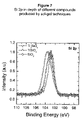
- FIG. 7 shows the Si 2p in depth of different compounds produced by sol-gel techniques
- FIG. 8 shows the binding energy of electron of different elements in different compounds
- FIG. 9 shows the O 1s in depth of different compounds produced by sol-gel techniques
- FIG. 10 shows the Ti 2p in depth of different compounds produced by sol-gel techniques
- FIG. 11 shows the dielectric constant and leakage current of TiSiOx films annealed at different temperatures
- FIG. 12 shows the variation in dielectric constant with frequency at different annealing temperatures
- FIG. 13 shows the variation in dissipation factor with frequency at different annealing temperatures
- FIG. 14 shows variation in dielectric constant with frequency at different annealing temperatures
- FIG. 15 shows variation in dissipation factor with frequency at different annealing temperatures
- FIG. 16 shows the leakage current with electric field at different annealing temperatures
- FIG. 17 shows the leakage current with annealing temperature at the electric field of 0.1 MV/cm
- FIG. 20 shows the dielectric constant with aging time for 1 MHz and 1 kHz
- FIG. 21 shows the dissipation factor with aging time for 1 MHz and 1 kHz
- FIG. 22 shows the J-E characteristics of TiSiO film with different aging time
- FIG. 23 shows the Leakage current density at 0.1 MV/cm electric field with different aging time
- FIG. 24 shows the variation in dielectric constant with frequency
- FIG. 36 shows the average dielectric constant and leakage current for different samples with variation of TiO 2 and SiO 2 in the films
- FIG. 37 shows the variation in dielectric constant with frequency for different silicate films
- FIG. 38 shows variation in the leakage current density with applied electric field for different silicate films
- FIG. 39 shows the variation in the current density with the electrical field for silicate films with various amount of SiO 2 in the films.
- FIG. 40 shows the variation in leakage current for silicate films with various amount of SiO 2 in the films.
- TiSiO 4 TiSiO y or (SiO 2 ) x (TiO 2 ) 1 ⁇ x mixed oxides.
- x were chosen as 0.25, 0.33, 0.5, 0.66 and 0.75.
- FTIR and XPS support the formation of Ti—O—Si bonding in all the silicate films irrespective of the value of x.
- the titanium silicate films were deposited on a substrate using conventional spin-on techniques referred to above.
- the deposited silicate films were annealed at 400° C., 500° C., 600° C., 700° C., 750° C. and 800° C. for a titanium silicate compound of (SiO 2 ) x (TiO 2 ) 1 ⁇ x with x is equal to 0.5 (i.e., TiSiO 4 ).
- the obtained average dielectric constant at 1 MHz is 23 ( ⁇ 1).
- the minimum leakage current at 0.1 MV/cm field is 2.1E ⁇ 7 A/cm 2 for the samples annealed at 600° C. Further prepared samples were annealed at 600° C. with x and the aging time of the sol varied.
- the minimum-leakage current density at 0.1 MV/cm was 2.0E ⁇ 7 A/cm 2 for samples produced from a sol which was aged for ⁇ 70 hrs.
- the average dielectric constant of silica-rich films i.e., (SiO 2 ) 0.75 (TiO 2 ) 0.25 molar
- SiO 2 ) 0.75 (TiO 2 ) 0.25 molar is of ⁇ 11 at 1 MHz, while they exhibit a very low leakage current density of 3.6E ⁇ 9 A/cm 2 at 0.1 MV/cm.
- the lowest leakage current of 4E ⁇ 8 A/cm 2 is obtained for the films obtained from the sol which has been aged for ⁇ 160 hrs.
- the sol-gel process involves the evolution of inorganic networks through the formation of a colloidal suspension (sol) and gelation of the sol to form a network in a continuous liquid phase (gel).
- the precursors for synthesizing these colloids consist of a metal or metalloid element surrounded by various reactive ligands.
- Metal alkoxides are most popular because they react readily with water.
- the most widely used metal alkoxides are the alkoxysilanes, such as tetramethoxysilane (TMOS) and tetraethoxysilane (TEOS).
- TMOS tetramethoxysilane
- TEOS tetraethoxysilane
- other alkoxides such as aluminates, titanates, and borates are also commonly used in the sol-gel process, often mixed with TEOS.
- sol-gel inorganic network At the functional group level, three reactions are generally used to describe the sol-gel process: hydrolysis, alcohol condensation, and water condensation. This general reaction scheme can be seen in FIG. 1 .
- the characteristics and properties of a particular sol-gel inorganic network are related to a number of factors that affect the rate of hydrolysis and condensation reactions, such as, pH, temperature and time of reaction, reagent concentrations, catalyst nature and concentration, H 2 O/Si molar ratio (R), aging, temperature and time, and drying.
- pH, nature and concentration of catalyst, H 2 O/Si molar ratio (R), and temperature have been identified as most important.
- Steric (spatial) factors exert the greatest effect on the hydrolytic stability of organoxysilanes. Any complication of the alkoxy group retards the hydrolysis of alkoxysilanes, but the hydrolysis rate is lowered the most by branched alkoxy groups.
- the effect of alkyl chain length and degree of branched are illustrated in the table of FIG. 3 taken from above reference: C. J. Brinker and G. S. Scherer, “Sol-gel Science” page 119, Academic Press, New York, 1990.
- the hydrolysis rate for Si(OEt)4 is 5 ⁇ 10 ⁇ 9 mol ⁇ 1 s ⁇ 1 and Ti(OR)4 is 1 ⁇ 10 ⁇ 3 mol ⁇ 1 s ⁇ 1 at pH 7, more than five order of magnitude greater.
- the condensation rate for Si(OEt)4 is 1 ⁇ 10 ⁇ 4 mol ⁇ 1 s ⁇ 1 where as for Ti(OEt)4 is 30 mol ⁇ 1 s ⁇ 1 was observed for TiO 2 formation.
- the recipe used for synthesizing titanium silicate films having 50% TiO2and 50% SiO 2 molar composition is shown in FIG. 4 .
- the obtained thickness of the films was ⁇ 200 nm on Pt/Si(100) substrates after annealing at 600° C.
- the table of FIG. 5 summarizes the amount of precursor used and catalysis as well as the refluxing time to synthesis of various mixed oxides.
- FTIR FTIR was used to identify the formation of titanium silicate in the films.
- Three characteristic peaks of Si—O—Si were observed in the IR spectroscopy for SiO 2 . These peaks were asymmetric stretching vibration mode at 1080 cm ⁇ 1 , bending mode at 810 cm ⁇ and rocking mode at 457 cm ⁇ 1 respectively.
- the characteristic signature of TiO 2 is the appearance of asymmetric stretching vibration of Ti—O—Ti mode at ⁇ 440 cm ⁇ 1 which overlaps with the rocking vibration of Si—O—Si mode. All films show the main peak of asymmetric Si—O—Si at 1060 cm ⁇ 1 .
- a distinct peak of Ti—O—Si is observed at 935 cm ⁇ 1 , which is the characteristic of the titanium silicate in the films as shown in FIG. 6 .
- the intensity ratio of Ti—O—Si to Si—O—Si peaks is seen to increase when the composition of the films is varied from TiO 2 towards TiSi 3 O x (see FIG. 6 ).
- FIG. 7 shows the binding energy of Si 2p in different compounds. Binding energy of Si 2p electron is less in the titanium silicate compound as compared to SiO 2 .
- Binding energy of O 1s in different silicate films has been presented in FIG. 9 .
- Binding energy of O 1s varies from 530.2 eV to 533 eV, which are the binding energies of TiO 2 and SiO 2 respectively.
- the table of FIG. 8 summarizes the binding energy of O 1s with the presence of SiO 2 in the samples. The FWHM of O 1s increases with the amount of SiO 2 in silicate films.
- FIG. 10 shows the Ti 2p 3/2 peak of different compounds along with TiO 2 after Ar ion etching.
- the peak width of Ti 2p 3/2 is found to reduce with the increase of SiO 2 in the films.
- the peak also shifts to a higher binding energy. This shifting of Ti 2p to higher binding energy confirms the formation of titanium silicate in the films.
- C K ⁇ ⁇ A d
- C the capacitance
- K the dielectric constant
- A the area
- d the thickness of the film
- the experimental parameters were:
- a sol was prepared and aged for ⁇ 70 hrs.
- a one layer film was deposited on platinum coated silicon substrates as well as on Si (100) substrates.
- the films were annealed in the oxygen atmosphere at 400° C., 500° C., 600° C. 700° C., 750° C. and 800° C. I–V and C–V measurements of the films are presented below.
- the dielectric constant of the films annealed at different temperatures is presented in the table of FIG. 11 .
- the average dielectric constant at 1 MHz is 23 ⁇ 1., which is nearly independent of the annealing temperature.
- the dielectric constant at low frequency (1 kHz) has a drastic variation from 130 to 25 as seen in the table of FIG. 11 .
- the dielectric constant and the dissipation factor of the films annealed at different temperatures are presented in FIG. 12 and FIG. 13 .
- the films annealed at 400° C. and 500° C. have a high relaxation as well as high dissipation factor at low frequencies.
- the relaxation as well as dissipation factor reduces after annealing the films at 600° C.
- the dielectric constant and dissipation factor increases slightly after increasing the annealing temperature to 700° C.
- FIG. 14 shows the change of dielectric constant at 1 kHz and 1 MHz with annealing temperatures.
- FIG. 15 shows the change of dissipation factor at 1 kHz and 1 MHz with annealing temperatures.
- the dissipation factor reaches a minimum.
- the dielectric constant of the films annealed at different temperatures is presented in table of FIG. 11 .
- the average dielectric constant at 1 MHz is 23 ⁇ 1., which is nearly independent of the annealing temperature.
- the dielectric constant at low frequency (1 kHz) has a drastic variation from 130 to 25 as seen in table of FIG. 11 .
- the dielectric constant and the dissipation factor of the films annealed at different temperatures are presented in FIG. 12 and FIG. 13 .
- the films annealed at 400° C. and 500° C. have a high relaxation as well as high dissipation factor at low frequencies.
- the relaxation as well as dissipation factor reduces after annealing the films at 600° C.
- the dielectric constant and dissipation factor increases slightly after increasing the annealing temperature to 700° C.
- FIG. 14 shows the change of dielectric constant at 1 kHz and 1 MHz with annealing temperatures.
- FIG. 15 shows the change of dissipation factor at 1 kHz and 1 MHz with annealing temperatures.
- the dissipation factor reaches a minimum value of 0.02 at 1 MHz for the samples annealed at 600° C. Dissipation factor starts increasing with the annealing temperatures and reaches 0.1 at 800° C. annealed samples, probably because of some Pt electrodes evolution.
- FIG. 16 shows the I–V characteristic of the TiSiO x films annealed at 400° C., 500° C., 600° C., 700° C., 750° C. and 800° C.
- FIG. 17 presents the leakage current density at the electric field of 0.1 MV/cm with annealing temperatures. Leakage current reduces with annealing temperature and attains minimum at 600° C. with the value of 2E ⁇ 7 A/cm 2 . Leakage current increases to 8E ⁇ 4 A/cm 2 when the annealing temperature is increased to 750° C. For useful results, the annealing temperature should lie in the range of about 500 to 700° C.
- the experimental parameters were:
- FIG. 18 and FIG. 19 show the variation of dielectric constant and dissipation factor as a function of frequency for various aging times. It is seen that the relaxation at lower frequencies reduces with the aging time.
- FIG. 20 summarizes the variation of dielectric constant at 1 kHz and 1 MHz with different aging time. The average dielectric constant in different aging time is 20.5 ( ⁇ 1.5) at 1 MHz. On the other hand the dielectric constant at 1 kHz is 27.0 ( ⁇ 3).
- the dissipation factor reduces with aging time and becomes minimum at 70–100 hrs (experiment performed at 67 hrs) of aging time as shown in FIG. 21 .
- the dissipation factor then starts increasing again with the aging time.
- the minimum of dissipation is observed to be 0.018 at the aging time of around ⁇ 67 hrs.
- the variation of dissipation factor at 1 KHz with the aging time has also been presented in FIG. 21 .
- FIG. 22 shows the variation of current density with the applied electric field for the films produced from the sol, which have been aged from 20 hrs to 167 hrs.
- FIG. 23 summarizes the variation of leakage current with the aging time for an applied electric field of 0.1 MV/cm. While the leakage current is of ⁇ 1E ⁇ 4 A/cm 2 , at 20 hrs of aging time, it becomes minimum ( ⁇ 2.0E ⁇ 7 A/cm 2 ) at aging time of 67 hrs and then increases again to 6.9E ⁇ 7 A/cm 2 as the aging time is increased to 142 hrs. As the aging time is further increased to 167 hrs, the leakage current slightly increases to 1.0E ⁇ 6 A/cm 2 . This variation of leakage current with aging time is very consistent with that of the dissipation factor.
- the experimental parameters were:
- FIG. 24 and FIG. 25 show the variation of dielectric constant and the dissipation factor as a function of frequency for various aging times.
- FIG. 26 shows the variation of dielectric constant at 1 kHz and 1 MHz with different aging time.
- the average dielectric constant at 1 MHz with five aging times (45, 96, 118, 142 and 163 hrs) is 38 ( ⁇ 1.5) as shown in FIG. 26 .
- Such a high value of the dielectric constant for the titanium silicate has not been reported in the literature. In the following publication: Nishiyama, A. Kaneko, M. Koyama, Y. Kamata, I. Fujiwara, M. Koike, M. Yoshiki and M. Koike, Mat. Res. Soc. Symp. Proc.
- rf-sputtered TiO 2 has a dielectric constant of about 39 and titanium silicate with composition (TiO 2 ) 0.57 (SiO 2 ) 0.43 has a dielectric constant about 29.
- the present inventors have found that the dielectric constant at 20 hrs aging time was around 66 and was not used for the averaging of the dielectric constant at 1 MHz.
- the dielectric constant at low frequency (1 kHz) was also found to reduce with aging time.
- the average dielectric constant of four samples (aged 96, 118, 142 and 163 hrs) at 1 kHz was about 51 ( ⁇ 4).
- the dissipation factor was also found to reduce with aging time as shown in the FIG. 27 .
- the dissipation factor is of ⁇ 0.3 while it decreases to a very low value of ⁇ 0.03 for the films made from sol aged 142 hrs.
- the dissipation factor of the films made from the sol aged for 163 increased to 0.05.
- FIG. 28 shows the variation of leakage current density with the electric field in different samples which have been made from various aged sols.
- the J-E curve is very similar and nearly independent of aging time.
- FIG. 29 shows the average leakage current for the five samples (20, 45, 96, 118 and 142 hrs) is of about 5.8E ⁇ 3 A/cm 2 .
- the experimental parameters were:
- FIG. 30 and FIG. 31 show the variation of dielectric constant and the dissipation factor with frequencies for different films produced from sol with various aging times.
- dissipation factor was found to increase slightly with the increase of frequencies, which is unusual.
- FIG. 32 and FIG. 33 show the variation of dielectric constant and dissipation factor at 1 kHz and 1 MHz with various aging time.
- the average dielectric constant (excluding 23 hrs sample which shows dielectric constant ⁇ 41 at 1 MHz) is 10.5 ⁇ 1.5 at 1 MHz and 12 ⁇ 2 at 1 kHz.
- the dissipation factor of 0.03 at 1 MHz for the sol aged for 144 hrs and 0.08 for the sample aged for 74 hrs are obtained.
- the dissipation factor at 2 kHz is 0.02, which is lower than the value obtained at 1 MHz.
- FIG. 35 shows the variation of leakage current with the aging time at the two different electric fields of 0.1 MV/cm and 1 MV/cm.
- the average leakage current for the films made from the sol aged between 96 hrs and 144 hrs is 3.6E ⁇ 9 A/cm 2 at an electric field of 0.1 MV/cm.
- the low leakage current of 3E ⁇ 8 A/cm 2 is obtained at 1 MV/cm field for the films obtained from the sol which has been aged for ⁇ 160 hrs.
- the dielectric constant of the titanium silicate reduces from 20.5 to 10.5 by changing the ratio of TiO 2 :SiO 2 from 1:1 to 1:3.
- This change of the composition is also concomitantly accompanied with a drastic reduction of the leakage current from ⁇ 5E ⁇ 7 to ⁇ 3E ⁇ 9 A/cm 2 , at an electric field of 0.1 MV/cm. Even at an electric field of 1 MV/cm, a leakage current as low as 3E ⁇ 8 A/cm 2 is obtained.
- the dielectric constant is found to reduce with the amount of SiO 2 in the films.
- the table of FIG. 36 shows the variation of dielectric constant (K) and leakage current with SiO 2 proportion in the silicate films. (Leakage current at 1 MV/cm is only obtained for the sample with 66 molar % and 75 molar % SiO 2 ).
- FIG. 37 shows the plots of dielectric constant as a function of frequency for the various film compositions. It is seen from the plots that the dielectric constant reduces with amount of SiO 2 in the films, at a given frequency.
- the dielectric constant of pure TiO 2 is found to be ⁇ 60. While adding 25 molar % SiO 2 in the films, the dielectric constant reduces to 38.
- the obtained dielectric constant is of about 21 when 50 molar % SiO 2 is added in the films. Dielectric constant further reduces to ⁇ 11 when the amount of SiO 2 increases to 75 molar % in the silicate films. This variation is summarized and plotted (red symbols) in FIG. 38 .
- FIG. 39 shows the leakage current density with applied electric field for different silicate film compositions (the corresponding data at 0.1 MV/cm are also summarized in Table 3.3).
- the leakage current density obtained for TiO 2 is 30.2E ⁇ 3 A/cm 2 ; while adding 25 molar % SiO 2 in the film, leakage current density reduces to 5.9E ⁇ 3 A/cm 2 .
- Leakage current density further reduces to 2.10E ⁇ 7 A/cm 2 after adding 50 molar % SiO 2 in the silicate films.
- Minimum leakage current of 2.5E ⁇ 9 A/cm 2 is obtained after adding 66 molar % SiO 2 in the films ( FIG. 40 ). At 1 MV/cm, the leakage current density was as low as 4.3E ⁇ 7 A/cm 2 and remains constant for the further addition of SiO 2 up to 75%.
Landscapes
- Chemical & Material Sciences (AREA)
- Engineering & Computer Science (AREA)
- Organic Chemistry (AREA)
- Materials Engineering (AREA)
- General Chemical & Material Sciences (AREA)
- Chemical Kinetics & Catalysis (AREA)
- Mechanical Engineering (AREA)
- Thermal Sciences (AREA)
- Physics & Mathematics (AREA)
- Metallurgy (AREA)
- Inorganic Chemistry (AREA)
- Life Sciences & Earth Sciences (AREA)
- Geochemistry & Mineralogy (AREA)
- Ceramic Engineering (AREA)
- Dispersion Chemistry (AREA)
- Formation Of Insulating Films (AREA)
- Inorganic Compounds Of Heavy Metals (AREA)
- Chemically Coating (AREA)
Abstract
Description
-
- Nishiyama, A. Kaneko, M. Koyama, Y. Kamata, I. Fujiwara, M. Koike, M. Yoshiki and M. Koike, Mat. Res. Soc. Symp. Proc. 670, K4.8.1 (2001)
- M. Koyama, A. Kaneko, M. Koike, I. Fujiwara, M. Yabuki, M. Yoshiki, M. Koike, and A. Nishiyama, Mat. Res. Soc. Symp. Proc. 670, K4.7.1 (2001)
- X. Wang, H. Masumoto, and Y. Someno, T. Hirai, Thin Solid Films 338, 105 (1999)
- M. F. Ouellette, R. V. Lang, K. L. Yan, R. W. Bertram, and R. S. Owles, J. Vac. Sci. Technol. A9, 1188 (1991)
- R. P. Netterfield, P. J. Martin, C. G. Pacey, and W. G. Sainty, J. Appl. Phys. 66, 1805 (1989)
-
- Y. Sorek, R. Reisfeld, I. Finkelstein, and S. Ruschin, Appl. Phys. Lett. 63, 3256 (1993)
- X. Orignac, D. Barbier, X. M. Du, and R. M. Almeida, Appl. Phys. Lett. 69, 895 (1996)
- A. M. Seco, M. C. Gongalves, and R. M. Almeida, Mater. Sci. Eng., B76, 193 (2000)
-
- It requires much less capital than the radio-frequency sputtering technique;
- It is capable of much higher throughput than the radio-frequency sputtering technique;
- It is capable of a self-planarizing effect on topography, which is an advantage if the titanium silicates are to be deposited on an integrated circuit already having high aspect ratio patterns. This factor is important since advanced CMOS, high voltage CMOS and/or intelligent MEMS devices generally have important surface topography and reactive sputtering is not well adapted to deposit such titanium silicates in the deep valleys formed by this important topology; i.e., the step coverage of reactively sputtered titanium silicates is generally very poor and preclude their use into such advanced devices;
- It allows a spin-on material from a liquid source and then much less prone to pin-holing following the evaporation of solvents;
- It allows two consecutive coats to be used as for the second coat to cover the residual pin-holes of the first coat;
- It is a very flexible technique to achieve well-oxidized TiO2/SiO2 alloys of various compositions.
-
- Molar weight of tetrabutoxytitanium(TBOT) [Ti(OC4H9)4] is 339.86 gm and density 0.998 gm/cc;
- Molar weight of tetraethoxysilicon (TEOS) [Si(OC2H5)4] is 208 gm and density 0.934 gm/cc;
- Molar weight of C2H5OH is 46 gm and density 0.80 gm/cc;
- Molar weight of H2O is 18 gm and density 1.0 gm/cc
where C is the capacitance, K the dielectric constant, A the area and d is the thickness of the film.
-
- TBOT:TEOS=1:1,
- TBOT=22.4×10⁻³ mole
- TEOS=22.4×10⁻³ mole
- Water (0.1 M HCl)=22.2×10⁻³ mole, (refluxing for 120 min at 70° C.)
- R=H2O/ TEOS=1
- Dilution 1:3 (Volume), 1 layer films, 2 steps drying (70° C./30 min and 120° C./30 min), annealed 600° C./1 hrs.
-
- TBOT:TEOS=1:1,
- TBOT=22.4×10⁻³ mole
- TEOS=22.4×10⁻³ mole
- Water (0.1 M HCl)=22.2×10⁻³ mole, (refluxing for 120 min at 70° C.)
- R=H2O/ TEOS=1
- Dilution 1:3 (Volume), 1 layer films, 2 steps drying (70° C./30 min and 120° C./30 min), annealed 600° C./1 hrs.
-
- TBOT:TEOS=3:1 (molar)
- TBOT=26.8×10⁻³ mole
- TEOS=8.96×10⁻³ mole
- C2H5OH=393×10−3 mole
- Water=20.2×10⁻³ mole
- R═H2O/TEOS=2.2
- Refluxing for 30 minutes at 70° C.
- Dilution 1:3 (Volume)
- 1 layer films
- 2 steps drying (70° C./30 min and 120° C./30 min)
-
Annealed 600° C./1 hrs
-
- TBOT:TEOS=1:3 (molar)
- TBOT=11.94×10⁻³ mole
- TEOS=35.84×10⁻³ mole
- C2H5OH=452×10−3 mole
- Water (0.1 M HCl)=37.8×10⁻³ mole
- R═H2O/TEOS=1
- Refluxing for 120 minutes at 70° C.
- Dilution 1:3 (Volume)
- 1 layer films
- 2 steps drying (70° C./30 min and 120° C./30 min)
-
Annealed 600° C./1 hrs
K=60−1.3x+0.01x 2
where x is the molar % of SiO2 in the film and K is the dielectric constant of the silicate films.
-
- Are deposited by the spin-on sol-gel technique using tetrabutoxytitanium (TBOT, Ti(OC4H9)4), and tetramethoxysilane (TEOS, Si(OC2H5)4) as precursors;
- Are annealed after deposition at temperatures between 500° C. and 700° C. in an oxygen containing atmosphere;
- Have a (SiO2)x(TiO2)1−x composition ranging between 0.50<x<0.75 (i.e.
- SiO2:TiO2 ranging between 1:1 and 3:1;
- Have a dielectric constant ranging between 10–50 at frequencies ranging between 1 kHz and 1 MHz;
- Have a dissipation factor ranging between 0.001 and 0.1 at frequencies ranging between 1 kHz and 1 MHz; and
- Have a leakage current ranging between 1 nA/cm2 and 1 μA/cm2 at an applied field ranging between 0.1 MV/cm and 1 MV/cm.
Claims (22)
Priority Applications (2)
| Application Number | Priority Date | Filing Date | Title |
|---|---|---|---|
| US10/864,472 US7101754B2 (en) | 2004-06-10 | 2004-06-10 | Titanium silicate films with high dielectric constant |
| EP05104951A EP1607375A3 (en) | 2004-06-10 | 2005-06-07 | Titanium silicate films with high dielectric constant |
Applications Claiming Priority (1)
| Application Number | Priority Date | Filing Date | Title |
|---|---|---|---|
| US10/864,472 US7101754B2 (en) | 2004-06-10 | 2004-06-10 | Titanium silicate films with high dielectric constant |
Publications (2)
| Publication Number | Publication Date |
|---|---|
| US20050277304A1 US20050277304A1 (en) | 2005-12-15 |
| US7101754B2 true US7101754B2 (en) | 2006-09-05 |
Family
ID=34980104
Family Applications (1)
| Application Number | Title | Priority Date | Filing Date |
|---|---|---|---|
| US10/864,472 Expired - Lifetime US7101754B2 (en) | 2004-06-10 | 2004-06-10 | Titanium silicate films with high dielectric constant |
Country Status (2)
| Country | Link |
|---|---|
| US (1) | US7101754B2 (en) |
| EP (1) | EP1607375A3 (en) |
Cited By (1)
| Publication number | Priority date | Publication date | Assignee | Title |
|---|---|---|---|---|
| US8940388B2 (en) | 2011-03-02 | 2015-01-27 | Micron Technology, Inc. | Insulative elements |
Families Citing this family (2)
| Publication number | Priority date | Publication date | Assignee | Title |
|---|---|---|---|---|
| TWI585249B (en) | 2016-04-25 | 2017-06-01 | 國立中央大學 | Nonlinear optical crystal and manufacturing method thereof |
| TWI846281B (en) * | 2023-01-18 | 2024-06-21 | 國立臺灣科技大學 | A deposition method, continuous deposition system and application thereof |
Citations (21)
| Publication number | Priority date | Publication date | Assignee | Title |
|---|---|---|---|---|
| US4849296A (en) * | 1987-12-28 | 1989-07-18 | Dow Corning Corporation | Multilayer ceramic coatings from metal oxides and hydrogen silsesquioxane resin ceramified in ammonia |
| US4997482A (en) * | 1987-01-02 | 1991-03-05 | Dow Corning Corporation | Coating composition containing hydrolyzed silicate esters and other metal oxide precursors |
| EP0433915A1 (en) | 1989-12-20 | 1991-06-26 | Central Glass Company, Limited | Method of forming metal oxide film by using metal alkoxide solution |
| US5270267A (en) | 1989-05-31 | 1993-12-14 | Mitel Corporation | Curing and passivation of spin on glasses by a plasma process wherein an external polarization field is applied to the substrate |
| US5320983A (en) | 1990-02-07 | 1994-06-14 | Mitel Corporation | Spin-on glass processing technique for the fabrication of semiconductor devices |
| US5447613A (en) | 1990-12-20 | 1995-09-05 | Mitel Corporation | Preventing of via poisoning by glow discharge induced desorption |
| US5457073A (en) | 1990-10-01 | 1995-10-10 | Mitel Corporation | Multi-level interconnection CMOS devices with SOG |
| US5470798A (en) | 1990-05-29 | 1995-11-28 | Mitel Corporation | Moisture-free sog process |
| US5753945A (en) * | 1995-06-29 | 1998-05-19 | Northern Telecom Limited | Integrated circuit structure comprising a zirconium titanium oxide barrier layer and method of forming a zirconium titanium oxide barrier layer |
| US6078493A (en) * | 1994-12-15 | 2000-06-20 | Samsung Electronics Co., Ltd. | Fin-shaped capacitor |
| US6083805A (en) | 1998-05-20 | 2000-07-04 | Mitel Corporation | Method of forming capacitors in a semiconductor device |
| US6268620B1 (en) | 1998-01-23 | 2001-07-31 | Mitel Corporation | Method of forming capacitors on integrated circuit |
| US6300144B1 (en) * | 1998-02-25 | 2001-10-09 | Interuniversitair Micro Elecktronica Centrum (Imec Yzw) | Method for fabricating ferro-electric thin films using a sol-gel technique |
| US6352889B1 (en) * | 1998-01-08 | 2002-03-05 | Matsushita Electric Industrial Co., Ltd. | Method for fabricating capacitor and method for fabricating semiconductor device |
| US6365266B1 (en) * | 1999-12-07 | 2002-04-02 | Air Products And Chemicals, Inc. | Mesoporous films having reduced dielectric constants |
| US20030011016A1 (en) * | 1999-05-12 | 2003-01-16 | Agarwal Vishnu K. | Multilayer electrode for ferroelectric and high dielectric constant capacitors |
| US6562408B1 (en) | 1998-09-09 | 2003-05-13 | Novara Technology S.R.L. | Process for preparing silica or silica-based thick vitreous films according to the sol-gel technique and thick films thereby obtained |
| US20030129315A1 (en) | 2000-05-18 | 2003-07-10 | Navin Suyal | Binders for coatings |
| US20040004982A1 (en) * | 2001-11-16 | 2004-01-08 | Eisler Hans J. | Nanocrystal structures |
| US20040003627A1 (en) * | 2002-07-03 | 2004-01-08 | Nihon Yamamura Glass Co., Ltd. | Locally crystallized glass |
| US7026694B2 (en) * | 2002-08-15 | 2006-04-11 | Micron Technology, Inc. | Lanthanide doped TiOx dielectric films by plasma oxidation |
-
2004
- 2004-06-10 US US10/864,472 patent/US7101754B2/en not_active Expired - Lifetime
-
2005
- 2005-06-07 EP EP05104951A patent/EP1607375A3/en not_active Withdrawn
Patent Citations (21)
| Publication number | Priority date | Publication date | Assignee | Title |
|---|---|---|---|---|
| US4997482A (en) * | 1987-01-02 | 1991-03-05 | Dow Corning Corporation | Coating composition containing hydrolyzed silicate esters and other metal oxide precursors |
| US4849296A (en) * | 1987-12-28 | 1989-07-18 | Dow Corning Corporation | Multilayer ceramic coatings from metal oxides and hydrogen silsesquioxane resin ceramified in ammonia |
| US5270267A (en) | 1989-05-31 | 1993-12-14 | Mitel Corporation | Curing and passivation of spin on glasses by a plasma process wherein an external polarization field is applied to the substrate |
| EP0433915A1 (en) | 1989-12-20 | 1991-06-26 | Central Glass Company, Limited | Method of forming metal oxide film by using metal alkoxide solution |
| US5320983A (en) | 1990-02-07 | 1994-06-14 | Mitel Corporation | Spin-on glass processing technique for the fabrication of semiconductor devices |
| US5470798A (en) | 1990-05-29 | 1995-11-28 | Mitel Corporation | Moisture-free sog process |
| US5457073A (en) | 1990-10-01 | 1995-10-10 | Mitel Corporation | Multi-level interconnection CMOS devices with SOG |
| US5447613A (en) | 1990-12-20 | 1995-09-05 | Mitel Corporation | Preventing of via poisoning by glow discharge induced desorption |
| US6078493A (en) * | 1994-12-15 | 2000-06-20 | Samsung Electronics Co., Ltd. | Fin-shaped capacitor |
| US5753945A (en) * | 1995-06-29 | 1998-05-19 | Northern Telecom Limited | Integrated circuit structure comprising a zirconium titanium oxide barrier layer and method of forming a zirconium titanium oxide barrier layer |
| US6352889B1 (en) * | 1998-01-08 | 2002-03-05 | Matsushita Electric Industrial Co., Ltd. | Method for fabricating capacitor and method for fabricating semiconductor device |
| US6268620B1 (en) | 1998-01-23 | 2001-07-31 | Mitel Corporation | Method of forming capacitors on integrated circuit |
| US6300144B1 (en) * | 1998-02-25 | 2001-10-09 | Interuniversitair Micro Elecktronica Centrum (Imec Yzw) | Method for fabricating ferro-electric thin films using a sol-gel technique |
| US6083805A (en) | 1998-05-20 | 2000-07-04 | Mitel Corporation | Method of forming capacitors in a semiconductor device |
| US6562408B1 (en) | 1998-09-09 | 2003-05-13 | Novara Technology S.R.L. | Process for preparing silica or silica-based thick vitreous films according to the sol-gel technique and thick films thereby obtained |
| US20030011016A1 (en) * | 1999-05-12 | 2003-01-16 | Agarwal Vishnu K. | Multilayer electrode for ferroelectric and high dielectric constant capacitors |
| US6365266B1 (en) * | 1999-12-07 | 2002-04-02 | Air Products And Chemicals, Inc. | Mesoporous films having reduced dielectric constants |
| US20030129315A1 (en) | 2000-05-18 | 2003-07-10 | Navin Suyal | Binders for coatings |
| US20040004982A1 (en) * | 2001-11-16 | 2004-01-08 | Eisler Hans J. | Nanocrystal structures |
| US20040003627A1 (en) * | 2002-07-03 | 2004-01-08 | Nihon Yamamura Glass Co., Ltd. | Locally crystallized glass |
| US7026694B2 (en) * | 2002-08-15 | 2006-04-11 | Micron Technology, Inc. | Lanthanide doped TiOx dielectric films by plasma oxidation |
Non-Patent Citations (2)
| Title |
|---|
| "Deposition of thick silica-titania sol-gel films on Si substrates", R.R.A. Syms et al., Journal of Non-Crystalline Solids 170 (1994) London, UK, 1994 Elsevier Science B.V., XP-002361077, pp. 223-233. |
| Brassard, D. et al: High-k titanium silicate thin films grown by reactive magnetron sputtering for CMOS. |
Cited By (1)
| Publication number | Priority date | Publication date | Assignee | Title |
|---|---|---|---|---|
| US8940388B2 (en) | 2011-03-02 | 2015-01-27 | Micron Technology, Inc. | Insulative elements |
Also Published As
| Publication number | Publication date |
|---|---|
| EP1607375A3 (en) | 2006-02-22 |
| EP1607375A2 (en) | 2005-12-21 |
| US20050277304A1 (en) | 2005-12-15 |
Similar Documents
| Publication | Publication Date | Title |
|---|---|---|
| US7112615B2 (en) | Porous material formation by chemical vapor deposition onto colloidal crystal templates | |
| DE60007769T2 (en) | DEPOSITION OF LAYERS USING ORGANOSILSESQUIOXANE PREPARATIONS | |
| KR100487968B1 (en) | Agriculture and pollution-resistant glass products | |
| US5801092A (en) | Method of making two-component nanospheres and their use as a low dielectric constant material for semiconductor devices | |
| US7186613B2 (en) | Low dielectric materials and methods for making same | |
| TWI284140B (en) | Method for forming porous silica film | |
| US20020190251A1 (en) | Thin film materials of amorphous metal oxides | |
| CN1544324A (en) | Preparation method of silica airgel film material | |
| TW201003785A (en) | Aminosilanes for shallow trench isolation films | |
| KR100367870B1 (en) | Method for the formation of a siliceous coating film and a substrate material provided with a siliceous coating film | |
| JPH05315319A (en) | Semiconductor device and its manufacture | |
| JP2003529202A (en) | Low dielectric nanoporous materials obtained from polymer decomposition | |
| US6809041B2 (en) | Low dielectric constant films derived by sol-gel processing of a hyperbranched polycarbosilane | |
| US7101754B2 (en) | Titanium silicate films with high dielectric constant | |
| WO2004074355A1 (en) | Low-permittivity material, and production and use thereof | |
| JP3919862B2 (en) | Method for forming low dielectric constant siliceous film and siliceous film | |
| US20030091748A1 (en) | Method for forming thin film from electrically insulating resin composition | |
| EP1855313A1 (en) | Process for producing modified porous silica film, modified porous silica film obtained by the process, and semiconductor device employing the modified porous silica film | |
| US7090896B2 (en) | Process for producing dielectric layers by using multifunctional carbosilanes | |
| JP4251927B2 (en) | Method for producing porous silica membrane | |
| CN108727020A (en) | A kind of PZT thin film and preparation method thereof | |
| JP2000077399A (en) | Silica-based porous membrane and method for producing the same | |
| US7446055B2 (en) | Aerosol misted deposition of low dielectric organosilicate films | |
| KR100572438B1 (en) | Coating method of automotive side mirror coated with photocatalyst oxide | |
| JPH09298241A (en) | Semiconductor device and manufacturing method thereof |
Legal Events
| Date | Code | Title | Description |
|---|---|---|---|
| AS | Assignment |
Owner name: DALSA SEMICONDUCTOR INC., CANADA Free format text: ASSIGNMENT OF ASSIGNORS INTEREST;ASSIGNORS:MY ALI, EL KHAKANI;DILIP, SARKAR K.;OUELLET, LUC;AND OTHERS;REEL/FRAME:016035/0138;SIGNING DATES FROM 20041112 TO 20041116 |
|
| STCF | Information on status: patent grant |
Free format text: PATENTED CASE |
|
| FPAY | Fee payment |
Year of fee payment: 4 |
|
| AS | Assignment |
Owner name: TELEDYNE DALSA SEMICONDUCTOR INC., CANADA Free format text: CHANGE OF NAME;ASSIGNOR:DALSA SEMICONDUCTOR INC.;REEL/FRAME:027064/0622 Effective date: 20110214 |
|
| FEPP | Fee payment procedure |
Free format text: PAYOR NUMBER ASSIGNED (ORIGINAL EVENT CODE: ASPN); ENTITY STATUS OF PATENT OWNER: LARGE ENTITY |
|
| FPAY | Fee payment |
Year of fee payment: 8 |
|
| MAFP | Maintenance fee payment |
Free format text: PAYMENT OF MAINTENANCE FEE, 12TH YEAR, LARGE ENTITY (ORIGINAL EVENT CODE: M1553) Year of fee payment: 12 |
|
| AS | Assignment |
Owner name: TELEDYNE DIGITAL IMAGING, INC., CALIFORNIA Free format text: MERGER;ASSIGNOR:TELEDYNE DALSA SEMICONDUCTOR INC.;REEL/FRAME:055434/0643 Effective date: 20210101 |