US7009680B2 - Narrow band tunable filter with integrated detector - Google Patents
Narrow band tunable filter with integrated detector Download PDFInfo
- Publication number
- US7009680B2 US7009680B2 US10/453,455 US45345503A US7009680B2 US 7009680 B2 US7009680 B2 US 7009680B2 US 45345503 A US45345503 A US 45345503A US 7009680 B2 US7009680 B2 US 7009680B2
- Authority
- US
- United States
- Prior art keywords
- tunable filter
- substrate
- liquid crystal
- filter
- pixel
- Prior art date
- Legal status (The legal status is an assumption and is not a legal conclusion. Google has not performed a legal analysis and makes no representation as to the accuracy of the status listed.)
- Expired - Lifetime, expires
Links
Images


Classifications
-
- G—PHYSICS
- G02—OPTICS
- G02F—OPTICAL DEVICES OR ARRANGEMENTS FOR THE CONTROL OF LIGHT BY MODIFICATION OF THE OPTICAL PROPERTIES OF THE MEDIA OF THE ELEMENTS INVOLVED THEREIN; NON-LINEAR OPTICS; FREQUENCY-CHANGING OF LIGHT; OPTICAL LOGIC ELEMENTS; OPTICAL ANALOGUE/DIGITAL CONVERTERS
- G02F1/00—Devices or arrangements for the control of the intensity, colour, phase, polarisation or direction of light arriving from an independent light source, e.g. switching, gating or modulating; Non-linear optics
- G02F1/01—Devices or arrangements for the control of the intensity, colour, phase, polarisation or direction of light arriving from an independent light source, e.g. switching, gating or modulating; Non-linear optics for the control of the intensity, phase, polarisation or colour
- G02F1/21—Devices or arrangements for the control of the intensity, colour, phase, polarisation or direction of light arriving from an independent light source, e.g. switching, gating or modulating; Non-linear optics for the control of the intensity, phase, polarisation or colour by interference
- G02F1/216—Devices or arrangements for the control of the intensity, colour, phase, polarisation or direction of light arriving from an independent light source, e.g. switching, gating or modulating; Non-linear optics for the control of the intensity, phase, polarisation or colour by interference using liquid crystals, e.g. liquid crystal Fabry-Perot filters
-
- G—PHYSICS
- G02—OPTICS
- G02F—OPTICAL DEVICES OR ARRANGEMENTS FOR THE CONTROL OF LIGHT BY MODIFICATION OF THE OPTICAL PROPERTIES OF THE MEDIA OF THE ELEMENTS INVOLVED THEREIN; NON-LINEAR OPTICS; FREQUENCY-CHANGING OF LIGHT; OPTICAL LOGIC ELEMENTS; OPTICAL ANALOGUE/DIGITAL CONVERTERS
- G02F2201/00—Constructional arrangements not provided for in groups G02F1/00 - G02F7/00
- G02F2201/30—Constructional arrangements not provided for in groups G02F1/00 - G02F7/00 grating
- G02F2201/307—Reflective grating, i.e. Bragg grating
-
- G—PHYSICS
- G02—OPTICS
- G02F—OPTICAL DEVICES OR ARRANGEMENTS FOR THE CONTROL OF LIGHT BY MODIFICATION OF THE OPTICAL PROPERTIES OF THE MEDIA OF THE ELEMENTS INVOLVED THEREIN; NON-LINEAR OPTICS; FREQUENCY-CHANGING OF LIGHT; OPTICAL LOGIC ELEMENTS; OPTICAL ANALOGUE/DIGITAL CONVERTERS
- G02F2201/00—Constructional arrangements not provided for in groups G02F1/00 - G02F7/00
- G02F2201/58—Arrangements comprising a monitoring photodetector
-
- G—PHYSICS
- G02—OPTICS
- G02F—OPTICAL DEVICES OR ARRANGEMENTS FOR THE CONTROL OF LIGHT BY MODIFICATION OF THE OPTICAL PROPERTIES OF THE MEDIA OF THE ELEMENTS INVOLVED THEREIN; NON-LINEAR OPTICS; FREQUENCY-CHANGING OF LIGHT; OPTICAL LOGIC ELEMENTS; OPTICAL ANALOGUE/DIGITAL CONVERTERS
- G02F2203/00—Function characteristic
- G02F2203/05—Function characteristic wavelength dependent
- G02F2203/055—Function characteristic wavelength dependent wavelength filtering
-
- G—PHYSICS
- G02—OPTICS
- G02F—OPTICAL DEVICES OR ARRANGEMENTS FOR THE CONTROL OF LIGHT BY MODIFICATION OF THE OPTICAL PROPERTIES OF THE MEDIA OF THE ELEMENTS INVOLVED THEREIN; NON-LINEAR OPTICS; FREQUENCY-CHANGING OF LIGHT; OPTICAL LOGIC ELEMENTS; OPTICAL ANALOGUE/DIGITAL CONVERTERS
- G02F2203/00—Function characteristic
- G02F2203/06—Polarisation independent
Definitions
- This invention generally relates to electrically tunable optical filters. More specifically, this invention relates to a polarization independent liquid crystal narrowband tunable filter with wide tuning range and integrated photodetector.
- Tunable optical filters are of particular importance because they can be configured to perform a variety of critical network functions, including channel selection and optical power monitoring.
- Prior art techniques to construct tunable optical filters include the acousto-optic tunable filter which operates by using an acoustic wave simulated by a radio-frequency power supply and transducer to induce densification and rarefaction in an optical waveguide material.
- acoustic-optic tunable filters usually work by changing the polarization of light at a wavelength that is matched to the acoustically induced grating which results in separation of tuned wavelength from the other wavelength components. Tuning is accomplished by changing the frequency of the applied acoustic wave.
- Acoustic-optic devices provide rapid tuning in the microsecond range and complete blanking of the filter, however they are not polarization independent devices and suffer from poor adjacent channel rejection and high insertion loss.
- optical nanostructures have been the object of scientific investigation for several years but advances in material science and imprint lithography have only recently resulted in their cost effective manufacturing and availability.
- An optical nanostructure is derived with feature sizes below the wavelength of light, so they offer uniform behavior over a broad wavelength, wide acceptance angles and unique optical properties by function of varying dimensions of the underlying grating features.
- optical nanostructures have been designed to function as a resonant waveguide, which, when coupled to an active layer capable of changing its index of refraction, is a foundation for tomorrows tunable waveguide filter.
- Liquid crystals are known to change their index of refraction with the application of voltage and can be dynamically controlled and configured to enable a range of optical switching and signal conditioning applications. Formed with opposing plates of sealed substrates, liquid crystal cells are considered a prospect technology and integration target capable of supplying the active layer to a nanostructure integrated therewith.
- Wang et. Al has recently demonstrated an experimental electrically tunable filter based on a waveguide resonant sub-wavelength nanostructure-grating filter incorporating a tuning mechanism in a thin liquid crystal.
- the device experiment was functional and exhibited performance of 30 nanometer tuning, however this device i) does not function in a polarization independent capacity; ii) does not offer a wide tuning range required for operation in different network bands, and; iii) does not address temperature stability issues associated with robust control of liquid crystal devices.
- liquid crystal based tunable filter over existing technologies include durability due to the absence of mechanical moving parts, no stretchable medium required as in prior art tunable filters and derivatives, no loss of optical performance in the event of mechanical failure, no fatigue resulting from mechanical failure occurring over time and the ability to provide tunable filter arrays with multiple tuning pixels.
- the present invention addresses a strong need for a low cost polarization independent tunable filter that offers a wide tuning range that operates in a reliable manner across a range of temperature and atmospheres.
- the present invention tunable filter utilizes active liquid crystal in conjunction with passive optical elements to vary the index of refraction of the media.
- a change in index of refraction creates different waveguide conditions and affects the incident light propagation in the media.
- Wavelength tuning is achieved from the liquid crystal material's ability to change the index of refraction as a function of an external electrical field.
- the present invention contains several features and embodiments that may be configured independently or in combination with other features of the present invention, depending on the application and operating configurations.
- the delineation of such features is not meant to limit the scope of the invention but merely to outline certain specific features as they relate to the present invention.
- liquid crystal tunable filter that may be constructed from materials substantially impervious to moisture.
- a liquid crystal tunable filter that utilizes active liquid crystal to tune a waveguide resonant grating filter in an architecture whereby polarization beam splitters and rotating mirrors separate and convert S- and P-polarization states into optically and geometrically parallel beams.
- the tunable filter may be configured with an extended tuning range by employing a 1 ⁇ N optical switch or splitter and N tunable pixel-filters, where N is an integer greater than one and where each pixel is a tunable filter having an offset center frequency enabling the tuning range of one pixel to partially overlap another pixel rendering the device and 1 ⁇ N switch capable of scanning pixels to yield an expanded continuous tuning range mode.
- the device may also employ, respectively, an optional deposited photodetector, deposited metal gasket moisture barrier bonding two opposing substrates each having a spacer layer to accurately control cell gap thickness; and, an integrated thermal sensor and heater deposition layer sandwiched between or deposited on at least one or both opposing substrates of the tunable filter.
- control system utilizing a time division scheme that multiplexes temperature sensing and heating functions across an integrated active thermal element in the tunable filter, such that the device may generally be kept at a constant temperature.
- a calibration process characterizes the profile of the device and generates a polynomial regression formula that provides the voltage drive output the platform based on the platform temperature and state of each pixel.
- the control system stores the state of the liquid crystal tunable filter, the regression formula, and reads the temperature of the device to compute and assert the temperature compensated voltage drive across the device.
- FIG. 1A shows a first embodiment polarization independent tunable filter utilizing birefringent walk off crystals and half wave plates to establish two reference inputs to a liquid crystal tunable filter.
- FIG. 1B shows the detailed liquid crystal tunable filter used in FIG. 1A .
- FIG. 1C shows the detailed liquid crystal tunable filter used in FIG. 1A with an optional integrated photodetector which may be used to capture all or tap a fixed percentage of the dual transmitted output.
- FIG. 1D shows a second embodiment polarization independent tunable filter pixel element in the X-Y plane that utilizes integrated polarization beam splitters to establish a two path pass through the filter and combine the outputs into single transmitted and reflected beams.
- FIG. 1E shows a second embodiment polarization independent tunable filter pixel element in the X-Y plane that utilizes integrated a polarization beam splitter to establish a two path pass through the filter and integrated photodetectors to capture all of tap a fixed percentage of the dual transmitted and reflected output beams.
- FIG. 1F shows a temperature sensor and heating device that may be integrated with any embodiment of the present invention.
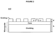
- FIG. 2 shows an example waveguide grating optical filter of the present invention.
- FIG. 3 shows an example tunable filter passband output profile as a function of index of refraction.
- FIG. 4 shows an example two-pixel tunable filter optical power monitor architecture having a tuning range substantially doubled over the range of any single pixel tuning element.
- FIG. 5 shows one process flow for fabricating the tunable filter of the present invention.
- FIGS. 6A and 6B show four pixel indium tin oxide (ITO) electrode forming masks of the present invention.
- FIGS. 7A and 7B show example integrated active thermal element forming masks of the present invention.
- FIGS. 8A and 8B show example spacer element forming masks of the present invention
- FIGS. 9A and 9B show example masks for defining a metal gasket element layer of the present invention.
- FIG. 10A shows an example top view integrated perspective showing the relationship between various layers of a one dimensional (1 ⁇ N) array configuration of the present invention.
- FIG. 10B is an isometric view showing a nine pixel (N ⁇ M) two dimensional liquid crystal cell at the termination of the fabrication process.
- FIG. 11 shows the liquid crystal thermal calibration and feedback loop method flows.
- FIG. 12 shows a block system diagram for the electronic control and thermal management system of the present invention.
- FIG. 1A shows a tunable filter 100 comprised of an input bi-directional optical polarization splitter/combiner 7 capable of accepting an input beam having any polarization and producing two substantially parallel output beams having the same polarization, a liquid crystal tunable filter pixel 101 having an input coupled to the output of the splitter/combiner that accepts the two beams and produces a reflected output passband as well as a passthrough complimentary transmission output beam for each input beam, and lastly, an output splitter/combiner 7 having an input that receives the output parallel passthrough transmission beams from the tunable pixel filter and produces a single output beam in response thereto.
- a tunable filter 100 comprised of an input bi-directional optical polarization splitter/combiner 7 capable of accepting an input beam having any polarization and producing two substantially parallel output beams having the same polarization
- a liquid crystal tunable filter pixel 101 having an input coupled to the output of the splitter/combiner that accepts the two beams and produces a reflected output passband
- the bi-directional optical splitter/combiners 7 may be comprised of a birefringent walk-off crystal 8 and half wave plate 41 .
- the birefringent crystal 8 accepts the input beam and separates it into two parallel paths each having orthogonal polarizations.
- the half wave plate 41 establishes parallel polarization from the two beams exiting the splitter/combiner 7 .
- one of the two parallel beams pass through the half waveplate to establish orthogonal polarization of the two beams such that when they pass through the birefringent crystal, the birefringent effect takes place and the beams converge at the output of the crystal.
- the tunable filter pixel 101 may be positioned anywhere from a >0 to 10 degree offset angle (alpha) Z-X plane to accommodate the preferred resonance mode and reflection path, however it is preferred that this angle be substantially 1 degree so that the reflected beam is decoupled from the incident beam but a liquid crystal and polyimide with reasonable pre-tilt can still be used.
- the passband output produced by the tunable filter pixel 101 overlaps the input path in the X-Z plane and deviates in the Y direction by an angle of 2*alpha.
- FIG. 1B shows a detailed configuration of a preferred liquid crystal tunable filter 101 that may be used in the first embodiment of the present invention.
- the liquid crystal tunable filter 101 may be comprised of a first substrate 110 A and a second substrate 110 B. It is essential that the first substrate has a layer stack in the aperture comprised of an electrode layer 104 A and waveguide resonant grating filter 117 . It is preferred that the present invention includes outside the aperture, a liquid crystal cell spacer layer 107 A and a metal gasket layer 106 A.
- the second substrate 110 B may contain an essential layer stack in the aperture comprised of an electrode layer 104 B and a liquid crystal anchor layer 109 B.
- the present invention includes a liquid crystal cell spacer layer 107 B and a metal gasket layer 106 B outside the aperture.
- the best mode of coupling the two substrates requires that the metal gasket 106 and spacer layers 107 on each substrate are coupled in opposition to each other to facilitate a bond between the two metal gasket layers to form a metal gasket seal 106 around the cell.
- a slight modification of the first embodiment of the present invention and herein included as part of the present invention is a configuration where the output bi-directional optical splitter/combiner 7 is eliminated and where one or more photodetector(s) capable of receiving the two transmitted and/or reflected output beams is coupled to the tunable pixel element 101 .
- Another slight modification of the first embodiment of the present invention and herein included as part of the present invention is a configuration where the output bi-directional optical splitter/combiner 7 is maintained but a one or more partially transparent photodetector(s) capable of tapping the two transmitted and/or the two reflected passband output beams is coupled to the tunable filter pixel 101 , as shown in FIG. 1C .
- FIG. 1D shows a polarization independent tunable filter pixel element 100 having a first substrate 110 A in opposition to a second substrate 110 B.
- the first substrate has, in the aperture, an essential inner surface layer stack comprising a polarization beam splitter 113 , a conductive electrode 104 and waveguide resonant grating filter 117 .
- an essential inner surface layer stack comprising a polarization beam splitter 113 , a conductive electrode 104 and waveguide resonant grating filter 117 .
- the second substrate 110 B has, in the aperture, an essential inner layer stack comprising a polarization beam splitter 113 B, a conductive electrode layer 104 B and a liquid crystal alignment layer 109 B.
- an patterned quarter wave rotating optical element 112 On the outer surface of the first substrate and in the aperture is an patterned quarter wave rotating optical element 112 .
- the optical beam will be rotated by one quarter wave as it enters and by one quarter wave as it exists the optical element 112 such that the total beam rotation is one half wave after reflection such that the output beam reflecting off of the polarization beam spitter/combiner 113 B is orthogonal to its counter part passing through the splitter 113 B and combining therewith to form the polarization maintained transmitted output beam.
- an optional metal gasket seal layer 106 B and spacer layer 107 B outside of the aperture on the inside surface of the second substrate. Liquid crystal molecules disposed in the aperture between the substrates 110 A and 110 B may be held in place by the metal gasket seal 106 .
- a slight modification of the second embodiment of the present invention utilizes integrated photodetectors to convert the photonic output of the tunable filter into an electrical signal. More specifically, a single photodetector may be used to capture the output of the paired parallel transmission beams and presented in FIG. 1 E. Alternately, a single photodetector may be used to capture the output of the reflected passband output and is as also shown in FIG. 1E . With respect to FIG. 1E , a polarization independent tunable filter pixel element 100 has a first substrate 110 A in opposition to a second substrate 110 B.
- the first substrate has, in the aperture, an essential inner surface layer stack comprising a polarization beam splitter 113 , a conductive electrode 104 and waveguide resonant grating filter 117 .
- an essential inner surface layer stack comprising a polarization beam splitter 113 , a conductive electrode 104 and waveguide resonant grating filter 117 .
- a patterned quarter wave rotating optical element 111 on the outer surface of the first substrate and in the aperture is a patterned quarter wave rotating optical element 111 .
- a quarter wave optical reflector will rotate the beam by one quarter wave as it enters and by one quarter wave as it exists the optical element 111 such that the total beam rotation is one half wave after reflection.
- both beams passing through the liquid crystal waveguide 117 have the same polarization states.
- an optional metal gasket seal layer 106 A and thin film spacer layer 107 A Outside the aperture on the inner surface of the first substrate.
- the second substrate 110 B has an essential inner layer stack in the aperture comprising a polarization beam splitter 113 B, a conductive electrode layer 104 B and a liquid crystal alignment layer 109 B.
- a photodetector element 128 On the outer surface of the second substrate and in the aperture is a photodetector element 128 that captures both polarization beam paths.
- an optional metal gasket seal layer 106 B and spacer layer 107 B outside of the aperture on the inside surface of the second substrate. Liquid crystal molecules disposed in the aperture between the substrates 110 A and 110 B may be held in place by the metal gasket seal 106 .
- All embodiments of the liquid crystal tunable filter pixel described herein can be configured to produce two outputs: a reflected passband output and a transmitted output.
- the reflected passband output is a Lorenzian shaped narrowband profile while the transmitted output is the compliment of the passband output.
- the input signal passes through the aperature of the cell and the passband output is reflected off the waveguide structure 117 (shown by way of dotted line).
- An input angle, alpha defines the optical path of the reflected passband output. Changes in this angle require a change in the grating period and/or waveguide material in order to maintain optimization over the same wavelength range.
- the reflected passband output has 2*alpha degrees of separation from the input beam and converges at the waveguide 117 .
- the transmitted output beam is a continuation of the input beam minus the reflected passband output.
- the second embodiment utilizes an alpha angle of 10 degrees to satisfy the optical path constraints implied by optical polarization beam splitter and combiner elements 111 and 112 , respectively.
- An important feature of the present invention is an integrated photodetector which may be placed at the reflected passband output and/or the transmitted output of the tunable filter.
- FIG. 1F shows a polarization independent tunable filter pixel element 100 having a first substrate 110 A in opposition to a second substrate 110 B.
- the first substrate has, in the aperture, an inner surface thin film layer stack comprising a polarization beam splitter 113 , a conductive electrode 104 layer and waveguide resonant grating filter 117 .
- a patterned quarter wave rotating optical element 111 is shown in FIG. 1F .
- the second substrate 110 B has, in the aperture, an inner layer stack comprising a polarization beam splitter 113 B, a conductive electrode layer 104 B and a liquid crystal alignment layer 109 B.
- a patterned quarter wave rotating optical element 112 On the outer surface of the first substrate and in the aperture is a patterned quarter wave rotating optical element 112 .
- an optional metal gasket seal layer 106 B, spacer layer 107 B and heater/temperature sensor element 108 outside of the aperture on the inside surface of the second substrate. Liquid crystal molecules disposed in the aperture between the substrates 110 A and 110 B may be held in place by the metal gasket seal 106 .
- the grating filter 117 consists of gratings on planar waveguide that are nominally transparent to an incident plane wave away from the resonance condition but reflect the externally incident plane wave at the resonance condition.
- E S t ⁇ E 0 + exp ⁇ ⁇ ( - i ⁇ ⁇ ⁇ ) ⁇ S ⁇ ⁇ exp ⁇ ( i ⁇ ⁇ ⁇ ) 1 -
- St is the diffraction coefficient that relates the incident wave to the wave initially transmitted through the waveguide
- ⁇ is the dephasing introduced by a deviation of the wavelength or incident angle at the resonance condition
- i is the incident wave
- E 0 is the energy transmitted away from resonance
- s is the diffraction coefficient relating the physical parameters of the waveguide grating (the Fresnel phase of waveguide interface, the dielectric constant difference in the grating region, the wave vector of the incident wave, the 1 st order Fourier components of the modulated dielectric constant of the grating, the depth of the grating surface relief, and the wave vectors in the liquid crystal and waveguide regions).
- the waveguide grating filter may comprise a grating and waveguide.
- the grating may be formed of silicon nitride.
- the grating period, P may be 200 to 900 nanometers depending on the frequency of operation, however it is preferred for telecommunications frequency applications in the C and L bands, that the period of the grating be 450 nanometers and depth, D, approximately 220 nanometers.
- the grating may be sourced from NanoOpto Inc. of Somerset New Jersey or formed by way of nano-imprint lithography or similar lithography processes as generally understood in the art or herein described.
- the waveguide may comprise a silicon nitride core approximately 480 nanometers thick and a silicon dioxide cladding approximately 1.5 microns thick.
- the index of refraction of the waveguide may be 2.3 to 3.05, it is preferred that the index of refraction be 2.95.
- the waveguide may also be sourced from NanoOpto Inc. of Somerset New Jersey or formed by way of thin film deposition as generally understood in the art.
- FIG. 3 shows the reflected passband and transition waveforms based on the aforementioned parameters.
- the tuning range of the liquid crystal tunable filter pixel of the present invention may exceed 100 nanometers.
- FIG. 4 A third embodiment of the present invention is shown in FIG. 4 , in which a multi-pixel tunable filter array disposed in a parallel configuration are used along with a passive splitter or active optical switch to route an input beam onto the plurality of tunable filter pixels.
- the tunable filters are formed with partially overlapping tuning ranges.
- the tunable filter array having overlapping tuning ranges may be fabricated by way of masking unique physical parameters for each tunable filter waveguide element in a master mask. It is preferred that the tuning ranges partially overlap to enable flexibility and tolerance in timing routines in the electronic control system (which will be described later in this application).
- One mode of operating the novel architecture of FIG. 4 is in an optical power monitoring mode, in which the firmware may sequentially scan across a single pixel until it reaches the end range (as shown as “B” in the first pixel of FIG. 4 ) at which point the firmware controller would actively switch the optical signal to the second pixel and take control the second pixel, engaging in a controlled scan across its tuning range, processing any photodetector output that may be coupled to the pixel.
- the optical splitter may alternately be replaced with a passive splitter for applications where optical losses are less critical.
- substrate 110 be comprised of glass but other substrate materials, including Garnet, silicon, polymers, etc., may be suitable depending on special pixel constructs and tailored tunable applications.
- FIG. 5 shows one example fabrication process to create the liquid crystal cell platform 100 .
- Various optional steps may be omitted depending on the embodiment of configured features.
- step one involves integrating the optical elements and layer stacks into the first and second substrates.
- the optical elements may be formed by way of nano-imprint lithography techniques or similar methods known in the field and including those based on impressing a reference mask into photo resist to create surface relief patterns on the substrate where the surface relief photo resist pattern is etched to form grating features in the nanometer range.
- the optical elements are deposited nanostructured gratings such as those available from NanoOpto Corporation of New Jersey who specifically offer the required optical elements, including the quarter wave reflector 111 , polarization beam splitters/combiner 113 and the waveguide resonant grating 117 .
- the optical elements including those referred to as 111 , 112 , 113 and 117 may be patterned and masked such that the specific optical functions are defined at referential pixel locations.
- the substrates are etched using nanoimprint lithography or similar methods known in the field and including those based on impressing a reference mask into photo resist to create surface relief patterns on the substrate where the surface relief photo resist pattern is etched to form grating features in the nanometer range.
- a uniform optical element mask may be used to pattern a global optical function across multiple pixels or the mask may be designed to provide local optical functions at referential pixel locations.
- the optical elements are preferably integrated into both surfaces of each substrate but they also may be supplied as a discreet chip and bonded to the target substrate by way of epoxy or other methods described herein or otherwise generally known.
- the deposition of a thin film photodetector optical elements 127 and 128 may be formed by way of iterative processes, including multiple deposition stages to apply the appropriate PIN diodes and based on amorphous, polycrystalline and microcrystalline materials for a completely absorbing photodetector, or silicon and germanium alloys for a partially transparent photodetector.
- Conductors for connecting to and contacting the photodetectors may be made from various transparent oxides, including zinc oxide, tin oxide and indium tin oxide.
- Step two involves adding the appropriate ITO (or other transparent conductive material) patterns to the first and second glass substrates to form the liquid crystal electrodes.
- a standard PECVD process may be used to apply thin film of ITO approximately 100 angstroms thick.
- FIGS. 6A and 6B show example ITO masks that may be used to pattern substrates 110 A and 110 B, respectively.
- Step three involves adding a polyimide alignment layer to the second substrate 101 B.
- standard spin coating stepped processes may be used at room temperature to create a layer of polyimide approximately 7000 angstroms thick on the second substrate.
- Step four involves patterning the polyimide layer.
- photo resist may first be applied to substrate 101 B and masked using traditional photolithography techniques or laser etching. Wet or dry etching performed thereafter may result in a pattern of polyimide.
- Step five involves anchoring the liquid crystal alignment layer.
- one traditional method is to rub the polyimide to form the alignment layers.
- the rubbing direction of the second substrate may be parallel to the equivalent homeotropic alignment provided by the grating waveguide filter 117 .
- a first alternate method of forming the second substrate alignment layer is to an imprint lithography technique where a reference mask is pressed onto a deposited photo resist layer to create surface relief patterns in the photo resist which is subsequently etched to form high precision alignment grooves with nanoscale tolerance.
- Steps three, four and five as mentioned above may be replaced by a second alternative method of the anchoring step and involves the use of a photo sensitive anchoring medium, such as Staralign by Vantio of Switzerland.
- the photosensitive anchoring medium may be spin applied to the substrate 110 B and masked to achieve specific anchoring energy and direction.
- UV light masking of various patterns, including specific directional application may be used to form individual pixels. Pixels may be formed with different rub characteristics, depending on the tunable application.
- Optional step six involves creating the active thermal element, integrated heater and temperature sensor.
- FIGS. 7A and 7B show example masks that may be use with respect to process step 206 of FIG. 5 , in which a seed adhesion layer of chrome is first deposited approximately 200 angstroms thick onto the substrates, followed by a PECVD deposition thin film platinum resistor layer approximately 2000 angstroms thick and forming the upper and lower portions of the integrated heater/temperature sensor.
- the upper and lower portions of the integrated device, applied to substrates 110 A and 110 B, may be separated by an air gap approximately 9.6 microns and interconnected by VIAS formed from a metal deposition step that will be described in succeeding step eight.
- gap thickness is delineated for example purposes and will change depending on the desired application.
- the platinum thin film resistor may be patterned in various shapes, including but not limited to arched, curved, circular, zigzag, stripped as well as the serpentine pattern of FIGS. 7A and 7B .
- the resistivity of the thin film platinum approximately 10.6E-8 ohm meters, the example shown yields approximately 100 ohms resistance at room temperature.
- Step seven involves creating the spacer element 107 .
- Spacer element 107 controls the gap thickness of the liquid crystal cell. While it is not necessary to equally distribute the spacer element equally on each substrate, it is preferred that one half of the desired gap thickness of the completed cell shall define the thickness of the spacer element 107 as deposited on each substrate. The combined cell 100 gap thickness may therefore be formed with a tolerance based on the deposition process.
- AL 2 O 3 is the preferred material for creating the spacer element, however other materials such as silicon dioxide, aluminum oxide, silicon nitride, silicon monoxide and other materials compatible with thin film deposition processes that do not substantially compress may also be used as an alternative to the silicon dioxide provided they are compatible with the selected liquid crystal substrate material.
- FIGS. 8A and 8B show an example mask that may be used to perform the process step 207 of FIG. 5 , where a patterned layer of 5 microns thick of silicon dioxide is deposited onto each substrate.
- Step eight involves creating the metal gasket element 106 .
- Metal gasket element 108 may be made from a variety of metals, including but not limited to, indium, gold, nickel, tin, chromium, platinum, tungsten, silver, bismuth, germanium and lead. However it is preferable to use a gold/tin composition because of its strength and melting temperature.
- FIGS. 9A and 9B show example masks that may be used to perform process step 208 of FIG. 5 , where, for the continuing example purpose, a layer approximately 7 to 9 microns thick of indium may equally be deposited on each substrate. It is generally preferable that metal gasket layer of this process step is deposited thicker than the spacer element of the previous step due to seepage that occurs during the additional processing steps.
- Metal gasket masks such as those shown in FIGS. 9A and 9B , may be configured to form referential VIAS 300 that enable electrical interconnection between features deposited on either substrate 110 A or 110 B.
- VIAS 300 may also be formed to simplify routing external contact pads to the temperature sensor and heating element.
- the VIAS 300 of the present example are positioned to overlap the heater/temperature sensor platinum layer defined in step six. They are also positioned to overlap the ITO layer so as to define contact pads to drive the two electrodes of the liquid crystal cell.
- Step nine involves aligning and pressing wafers 110 A together with 110 B.
- visual alignment reference marks may be etched into the underlying wafer, or that a physical feature of the glass sheet such as an edge or alignment hole may be used to perform wafer alignment.
- a high yield method of accurately aligning the relative position of the two glass substrates without the need for expensive high precision alignment equipment is hereby presented, in which complimentary interlocking geometric features deposited on each substrate, mate with each other to prevent relative movement of the glass sheets during the bonding and pressing process.
- Such interlocking features mitigate any non uniformity in the bonding process and given that the typical gap between two glass sheets of a liquid crystal cell is less than 20 micrometers, thin film deposition or screening processes can be used to create precisely controlled and repeatable geometric features.
- the substrates 110 A and 110 B may be brought together, aligned under pressure at room temperature to form a chemical bond metal gasket at the gap distance defined by the sandwich spacer elements formed from both substrates.
- Step ten involves dicing of the wafers.
- Process step 210 of FIG. 5 may be performed using a dicing saw or via etching techniques.
- Step 11 involves removal of a portion of protective glass on the liquid crystal cell.
- FIG. 10A shows a top perspective of the various layers that combine through the substrates when interposed thereupon each other in a fully configured embodiment of the present invention.
- the substrate 110 B is scored using a diamond dicing saw to cut a trench approximately 90% through the thickness of the substrate and forming the break off line 119 of FIG. 10A .
- a portion of the substrate 110 B is broken off along the break off line 119 to define an access surface 113 of FIG. 10B that provides access to the underlying liquid crystal electrode contact pads 500 and 500 ′, the underlying liquid crystal heater/temperature sensor element electrical contact pads 502 and 502 ′, as well as to the liquid crystal fill port 115 .
- Step 12 involves filling the liquid crystal device with a liquid crystal molecules, process 212 of FIG. 5 .
- This step may be performed using traditional methods of filling a liquid crystal cell, whereby the cell is placed in a vacuum, a droplet size of liquid crystal material is placed at the fill port 115 , and with the release of the vacuum, equilibrium pressure forces the liquid crystal material into the fill port 115 and the fill port is plugged.
- Several techniques to cap the fill port including UV curable epoxy which may be used to close the fill port.
- the present invention includes various liquid crystal configurations designed to function in a variety of specific optical systems and applications. More specifically, the tunable filter may be tailored for specific optical applications, including, but not limited to spectroscopy and optical power monitoring applications.
- any non-linearity in changing the center wavelength of the filter may be algorithmically compensated using a slightly modified thermal calibration and operating processes of the present invention in which a three dimensional curve fit is used to model a parameter space including either wavelength versus voltage and temperature or wavelength versus switching time transition and temperature. This modification will be evident upon review of the thermal compensation calibration and operating loop now described:
- FIGS. 11 and 12 A block diagram of the control system and components directed to a liquid crystal tunable filter are included in FIGS. 11 and 12 along with the liquid crystal thermal management and voltage controller subsystems of the present invention, now described in further detail.
- host computer 400 may be configured to communicate with microcontroller 402 over a full duplex data interface and enabling the host computer to engage functions, send commands and retrieve data from microcontroller 402 .
- Microcontroller may be configured to store software control routines. The software control routines may function to adjust voltage drive provided to each pixel in the liquid crystal cell in response to temperature fluctuations.
- the microcontroller may utilize a time division multiplexing scheme that multiplexes temperature sensing and heating functions in the integrated sensor/heater device such that the cell may generally be kept at a constant temperature.
- a calibration process characterizes the profile of the cell and generates a polynomial regression formula that provides the optimal voltage drive output for given temperature and cell state inputs.
- the microcontroller 402 stores the state of the liquid crystal cell, the regression formula, and reads the temperature of the liquid crystal cell to compute and assert the temperature compensated voltage drive.
- FIG. 11 shows a calibration process that may be used to perform the method of the present invention in which a liquid crystal cell thermal operating characteristic profile is translated into deterministic coefficients assembled into a stored regression formula used to adjust the voltage drive to the cell in response to temperature and cell state.
- the first step to determine the coefficient values in the cell's temperature and voltage compensation profile is to profile the liquid crystal cell drive characteristics across a range of temperatures.
- the profile process step 601 may examine a light source passing through the cell and its center wavelength at a given voltage and temperature combination.
- An operational liquid crystal cell is placed in a thermal chamber programmed to change operating temperature across the desired temperature range at a given interval.
- a range of voltages are provided to the liquid crystal cell while a performance characteristic, such as center wavelength, is measured.
- Voltage is scanned until to achieve maximum spectra range, at which point the voltage, center wavelength and temperature levels are stored as a grid reference in a cell profile definition table.
- the performance of the liquid crystal cell is recorded at grid point center wavelength and temperature levels, resulting in a multi dimensional lookup table whereby any temperature and voltage input provides an center wavelength level output.
- This table may be represented as a three dimensional surface.
- the power versus time profile is measured at each temperature as the voltage is scanned from maximum to minimum, and visa versa.
- the second step requires processing the lookup table to smooth the voltage profile over temperature and the time profile over temperature at the given center wavelength levels as recorded in the previous step.
- a statistical program capable of performing regression analysis such as Mathematica® may be used to perform this process step 602 .
- . . v n a n +b n T+c n T 2 +d n T 3 +e n T 4
- V voltage
- T liquid crystal cell temperature
- a,b,c,d,e curve fit coefficients
- n attenuation level.
- step three results in smooth curve regressions fit across orthogonal axis of the three dimensional surface, whereby the smooth curves are fit over the coarse center wavelength grid recorded in step 1 .
- step 603 the five coefficients of the previous step are each solved by a second order regression.
- Theta liquid crystal center wavelength
- Step four is the final step in the calibration process of FIG. 11 , process 606 , and results in storing the coefficients in the liquid crystal control system which is now described.
- the coefficients that profile the liquid crystal characteristics may be stored in microcontroller 402 memory ( FIG. 12 ) by flashing the memory of the microcontroller with the appropriate 15 coefficient values.
- the thermal compensation system of the present invention could operate by reading the temperature of the liquid crystal cell and adjusting the voltage drive of the cell based on the cell state.
- the cell state may typically be at any center wavelength in the spectral range.
- the cell state may be stored in the microcontroller 402 and also be configured via the host computer 400 .
- voltage can be applied directly from minimum to maximum and the temperature calibration is used to correlate center wavelength versus time.
- Microcontroller may be a PIC microchip having an internal analog digital converter and operating with a 10 Mhz crystal oscillator 404 clock.
- the microcontroller may be programmed to cycle through all pixels in the cell to controllably apply voltage to each pixel.
- the microcontroller may be connected to a multi-channel digital analog converter (DAC) configured to provide an output voltage level in response to a configuration pulse stream from the microcontroller over a serial interface.
- the output of the DAC connects to the input of an analog switch array having switching element 414 n associated with each pixel in the cell.
- Each element in the switch array 414 preferably shares a 1.2 khz clock provided by an output port pin of the microcontroller.
- a frequency modulated drive may be incorporated into the platform to replace the amplitude modulated voltage drive.
- Such FM drive may also be optimized using the same methodology as described later in the thermal compensation calibration and operation loops.
- DATA is passed to the DAC along with a SELECT pulse train encoding the appropriate voltage amplitude at the Nth output channel.
- a WR command sent to the DAC causes the DAC output to be received at the input of the Nth analog switch 414 n , triggering the application of an AM transmission over a 1.2 khz carrier to be applied to the appropriate liquid crystal cell electrode 500 N .
- N is incremented and the voltage is applied the next pixel in the system.
- a temperature sensor reading may be provided by the internal integrated heater/temperature sensor from an external device.
- One of the heater/temperature sensor electrodes 502 or 502 ′ of the liquid crystal cell 100 may be grounded while the other may connect to switch 407 .
- Switch 407 may selectively engage the integrated heater/temperature sensor element 108 in a sense or heat mode. More specifically, switch 407 may be configured ON to connect the ungrounded heater/temperature electrode through instrumentation amplifier 406 to an ADC coupled to the microcontroller which reads the temperature on the liquid crystal cell, or it may be configured OFF so that power amplifier FET 410 , which may be controlled by a pulse train from microcontroller 402 and applies a voltage potential to operate the device 108 as a heater.
- the microcontroller reads the temperature of the liquid crystal cell and calculates the voltage drive based on the sensed temperature, T, and the current state of each pixel, Theta.
- v ( X+Y ⁇ +Z ⁇ 2 )+ ( X 1 +Y 1 ⁇ +Z 1 ⁇ 2 ) T+ ( X 2 +Y 2 ⁇ +Z 2 ⁇ 2 ) T 2 + ( X 3 +Y 3 ⁇ +Z 3 ⁇ 2 ) T 3 + ( X 4 +Y 4 ⁇ +Z 4 ⁇ 2 ) T 4
- the new voltage value V is stored in the microcontroller for transmission to the DAC 412 during the next voltage application cycle.
- the time calibration method is applicable to all of the above steps where, again, time is the variable replacing voltage.
- the liquid crystal cell may also be maintained about a reference temperature.
- Process step 609 with respect to FIG. 11 involves the application of heat to maintain the temperature of the liquid crystal cell about a reference temperature.
- the reference temperature may be above the ambient room temperature or above the temperature of any carrier device that may be coupled to the liquid crystal cell. The selection of a reference temperature above the ambient temperature will result in the tendency of the liquid crystal cell to cool to meet the ambient temperature after the application of a heat burst. A counter thermal bias is therefore generated to support temperature stability about the reference temperature.
- Microcontroller memory may store the reference temperature, the value of the current temperature, historical temperatures, and, historical levels of heat applied to the liquid crystal cell.
- the value of the sensed temperature T at every instance may be compared against the reference temperature to determine the amount of heat to apply to the liquid crystal cell.
- An 8 bit analog digital converter will provide approximately 1 ⁇ 3 of a degree of temperature sensing resolution over the desired temperature range, so the example system may provide for temperature stability about a reference temperature to within 1 ⁇ 3 degree Celsius.
- a threshold detector routine stored in microcontroller ROM may trigger a control function if the sensed temperature of the liquid crystal cell falls below the desired operating reference temperature. The control function may determine how much heat to apply to the liquid crystal cell.
- the control function may utilize error minimizing routines that track the change in temperature across multiple instances of process step 609 .
- the error correcting routines may store the previous temperature reading T 0 along with the previous amount of heat applied to the liquid crystal cell H 0 .
- the temperature reading and every succeeding temperature reading T 1 may be compared against T 0 to determine the amount of temperature change resulting from the previous heating of the liquid crystal cell.
- Heat may be applied to the liquid crystal cell by way of the FET power driver as described above.
- the heater may be triggered at a fixed or variable duty cycle and controlled using frequency or amplitude modulation.
- the polarization beam splitting element 113 and the conductive electrode 104 can be applied in reverse order such that the conductive electrode 104 is directly adjacent to the substrate and the polarization beam splitting element is directly a top thereof.
- Various patterns may be used to form the spacer element, metal gasket and integrated heater/temperature sensor elements of the multi-pixel cell platform. Use of external temperature sensors and heaters in part or whole may be applied using the temperature compensation methods and regression of the present invention.
- the conductive electrode layer 104 may be transparent or reflective, depending on the application and pixel type.
- the metal gasket may be modulated to provide heating function in addition to its function as a moisture barrier support membrane.
- Epoxy gaskets may be used in combination with metal gasket elements in part or whole, and the metal gasket elements may comprise a single solder cap.
- Anchoring and aligning the liquid crystal material in a cell may also be performed using photo alignment material, Staralign by Vantio of Switzerland or other known alignment methods, including laser etching. Anchoring the liquid crystal material in the cell (described hereunder as step five) may be performed before patterning of the polyimide (described hereunder as step four).
- the process steps for the closed loop temperature feedback may also be rearranged such that the heating process is performed prior to applying the voltage drive.
- the order of fitting voltage with each dimension of the three dimensional surface is reversible and other three dimensional surface fitting algorithms may be used, including but not limited to those that describe a surface with one dimension fitting a fourth degree polynomial and the other dimension fitting a second degree polynomial. Amplitude or frequency modulation may be used to tune the liquid crystal tunable filter. It is well within the scope of the present invention to make modifications to the electrode masks to produce any size array of liquid crystal cells in any first, second or third dimension. Finally, it is well within the scope of the present invention to change the electrode masks accordingly to modify the shape of each pixel.
Landscapes
- Physics & Mathematics (AREA)
- Nonlinear Science (AREA)
- Chemical & Material Sciences (AREA)
- Crystallography & Structural Chemistry (AREA)
- General Physics & Mathematics (AREA)
- Optics & Photonics (AREA)
- Liquid Crystal (AREA)
- Optical Modulation, Optical Deflection, Nonlinear Optics, Optical Demodulation, Optical Logic Elements (AREA)
Abstract
Description
2k 2 h+2φ12+2φ23=2mπ
where m is the mode number, k2 is the wave vector of light in the x direction in the waveguide, h is the waveguide thickness and φ12 and φ23 are the two Fresnel phases due to the waveguide interface internal reflections.
The grating on top of the
K=2π/Λ
where Λ is the grating period and the value of the grating vector K is approximately the same as that of the mode propagation constant in the z direction, β, which is
β2=ε2 k 0 2 −k 2 2,
where k0 is the wave vector of the incident wave, k2 is the wave vector of light in the x direction in the waveguide, and ε2 is the dielectric constant in the waveguide. As so, the total destructive interference at resonance will obtain a total output transmitted field E, given by
v=a+bT+cT 2 +dT 3 +eT 4
v 1 =a 1 +b 1 T+c 1 T 2 +d 1 T 3 +e 1 T 4
v 2 =a 2 +b 2 T+c 2 T 2 +d 2 T 3 +e 2 T 4
.
.
.
v n =a n +b n T+c n T 2 +d n T 3 +e n T 4
where V=voltage, T=liquid crystal cell temperature, a,b,c,d,e=curve fit coefficients, and n=attenuation level.
v=a+bT+cT 2 +dT 3 +eT 4, where,
a=(X+Yθ+Zθ 2)
b=(X 1 +Y 1 θ+Z 1θ2)
c=(X 2 +Y 2 θ+Z 2θ2)
d=(X 3 +Y 3 θ+Z 3θ2)
e=(X 4 +Y 4 θ+Z 4θ2)
v=(X+Yθ+Zθ 2)+
(X 1 +Y 1 θ+Z 1θ2)T+
(X 2 +Y 2 θ+Z 2θ2)T 2+
(X 3 +Y 3 θ+Z 3θ2)T 3+
(X 4 +Y 4 θ+Z 4θ2)T 4
Claims (23)
Priority Applications (4)
| Application Number | Priority Date | Filing Date | Title |
|---|---|---|---|
| US10/453,455 US7009680B2 (en) | 2003-06-02 | 2003-06-02 | Narrow band tunable filter with integrated detector |
| US10/607,855 US20060007386A1 (en) | 2003-02-21 | 2003-06-27 | Flat top tunable filter with integrated detector |
| US10/719,078 US7221429B1 (en) | 2003-06-02 | 2003-11-21 | Wavelength locker with liquid crystal tunable filter generating transmitted and reflected outputs |
| US12/349,981 US20090195715A1 (en) | 2003-02-21 | 2009-01-07 | Flat top tunable filter with integrated detector |
Applications Claiming Priority (1)
| Application Number | Priority Date | Filing Date | Title |
|---|---|---|---|
| US10/453,455 US7009680B2 (en) | 2003-06-02 | 2003-06-02 | Narrow band tunable filter with integrated detector |
Related Parent Applications (1)
| Application Number | Title | Priority Date | Filing Date |
|---|---|---|---|
| US10/391,510 Continuation-In-Part US7046326B2 (en) | 2003-02-21 | 2003-03-17 | Multi-pixel liquid crystal cell array |
Related Child Applications (2)
| Application Number | Title | Priority Date | Filing Date |
|---|---|---|---|
| US10/607,855 Continuation-In-Part US20060007386A1 (en) | 2003-02-21 | 2003-06-27 | Flat top tunable filter with integrated detector |
| US10/719,078 Continuation US7221429B1 (en) | 2003-06-02 | 2003-11-21 | Wavelength locker with liquid crystal tunable filter generating transmitted and reflected outputs |
Publications (2)
| Publication Number | Publication Date |
|---|---|
| US20040239869A1 US20040239869A1 (en) | 2004-12-02 |
| US7009680B2 true US7009680B2 (en) | 2006-03-07 |
Family
ID=33452124
Family Applications (2)
| Application Number | Title | Priority Date | Filing Date |
|---|---|---|---|
| US10/453,455 Expired - Lifetime US7009680B2 (en) | 2003-02-21 | 2003-06-02 | Narrow band tunable filter with integrated detector |
| US10/719,078 Expired - Lifetime US7221429B1 (en) | 2003-06-02 | 2003-11-21 | Wavelength locker with liquid crystal tunable filter generating transmitted and reflected outputs |
Family Applications After (1)
| Application Number | Title | Priority Date | Filing Date |
|---|---|---|---|
| US10/719,078 Expired - Lifetime US7221429B1 (en) | 2003-06-02 | 2003-11-21 | Wavelength locker with liquid crystal tunable filter generating transmitted and reflected outputs |
Country Status (1)
| Country | Link |
|---|---|
| US (2) | US7009680B2 (en) |
Cited By (12)
| Publication number | Priority date | Publication date | Assignee | Title |
|---|---|---|---|---|
| US20050078237A1 (en) * | 2001-12-06 | 2005-04-14 | Werner Klaus | Liquid crystal variable wavelength filter unit, and driving method thereof |
| US20060007386A1 (en) * | 2003-02-21 | 2006-01-12 | Extellus Usa | Flat top tunable filter with integrated detector |
| US20070071061A1 (en) * | 2003-12-24 | 2007-03-29 | Giulia Pietra | Tunable resonant grating filters |
| US20090008736A1 (en) * | 2007-07-05 | 2009-01-08 | National Taiwan University | Method for photo-detecting and apparatus for the same |
| US20090014632A1 (en) * | 2007-07-10 | 2009-01-15 | Cambridge Research & Instrumentation, Inc. | Athermalized birefringent filter apparatus and method |
| US20090022448A1 (en) * | 2007-07-16 | 2009-01-22 | Wei Wu | Optical device including waveguide grating structure |
| US20090034899A1 (en) * | 2007-07-30 | 2009-02-05 | David Fattal | Optical modulator including waveguide grating structure and multiple quantum well layer |
| WO2008068753A3 (en) * | 2006-12-04 | 2009-09-03 | Ben-Gurion University Of The Negev - Research And Development Authority | Polarization independent birefringent tunable filters |
| US20110043742A1 (en) * | 2003-02-21 | 2011-02-24 | Cavanaugh Shanti A | Contamination prevention in liquid crystal cells |
| US20160299333A1 (en) * | 2015-04-09 | 2016-10-13 | Goodrich Corporation | Optical sensors |
| US11009398B2 (en) * | 2018-05-30 | 2021-05-18 | Samsung Electronics Co., Ltd. | Tunable optical filter based upon liquid crystal cell and wavelength sweeping method |
| US11199735B2 (en) * | 2019-03-28 | 2021-12-14 | Lumcolor | Smart optical filter for pixel-selectively adjusting light intensity |
Families Citing this family (21)
| Publication number | Priority date | Publication date | Assignee | Title |
|---|---|---|---|---|
| US7389043B2 (en) * | 2003-10-31 | 2008-06-17 | Nortel Networks Limited | Protection architecture for photonic switch using tunable optical filter |
| JP2006243782A (en) * | 2005-02-28 | 2006-09-14 | Toshiba Corp | Information processing apparatus and control method thereof |
| US7474396B2 (en) * | 2006-01-17 | 2009-01-06 | Hewlett-Packard Development Company, L.P. | Raman spectroscopy system and method using a subwavelength resonant grating filter |
| US7524073B2 (en) * | 2006-11-16 | 2009-04-28 | Canon Kabushiki Kaisha | Layered periodic structures with peripheral supports |
| US8340523B2 (en) * | 2008-02-20 | 2012-12-25 | Jds Uniphase Corporation | Tunable optical filter |
| KR101689817B1 (en) | 2008-06-21 | 2017-01-09 | 렌즈벡터 인코퍼레이티드 | Electro-optical devices using dynamic reconfiguration of effective electrode structures |
| US8033054B2 (en) * | 2008-06-21 | 2011-10-11 | Lensvector Inc. | Electro-optical devices using dynamic reconfiguration of effective electrode structures |
| US20100322269A1 (en) * | 2009-06-17 | 2010-12-23 | Cogo Optronics, Inc. | Tunable laser |
| US8064745B2 (en) * | 2009-11-24 | 2011-11-22 | Corning Incorporated | Planar waveguide and optical fiber coupling |
| US8582115B2 (en) * | 2010-10-07 | 2013-11-12 | Omnivision Technologies, Inc. | Tunable and switchable multilayer optical devices |
| CA2863983C (en) | 2012-02-10 | 2022-05-10 | Nkt Photonics A/S | Laser device with frequency stabilising control module |
| US20140293393A1 (en) | 2013-03-28 | 2014-10-02 | Barthelemy Fondeur | Flat-top tunable filter |
| US9207516B1 (en) * | 2013-08-29 | 2015-12-08 | Mozhi Yu | Hybrid tunable filter capable of outputting a single spectral peak |
| CN103792658B (en) * | 2014-02-18 | 2016-03-30 | 苏州旭创科技有限公司 | Optical standard tool |
| US10146094B2 (en) * | 2014-08-17 | 2018-12-04 | Ibrahim Abdulhalim | Tunable achromatic waveplates |
| WO2016081906A1 (en) * | 2014-11-20 | 2016-05-26 | Oe Solutions America, Inc. | Method and apparatus for controlling, monitoring, and communicating with tunable optical devices and subassemblies |
| US9632226B2 (en) | 2015-02-12 | 2017-04-25 | Digilens Inc. | Waveguide grating device |
| EP3548939A4 (en) | 2016-12-02 | 2020-11-25 | DigiLens Inc. | WAVE GUIDE DEVICE WITH UNIFORM OUTPUT LIGHTING |
| WO2019046649A1 (en) * | 2017-08-30 | 2019-03-07 | Digilens, Inc. | Methods and apparatus for compensating image distortion and illumination nonuniform ity in a waveguide |
| CN108761891A (en) * | 2018-06-19 | 2018-11-06 | 北京航空航天大学 | A kind of wide range polarization grating optimization method based on compensation of refractive index |
| US20200247017A1 (en) | 2019-02-05 | 2020-08-06 | Digilens Inc. | Methods for Compensating for Optical Surface Nonuniformity |
Citations (42)
| Publication number | Priority date | Publication date | Assignee | Title |
|---|---|---|---|---|
| US4135789A (en) | 1977-07-01 | 1979-01-23 | Beckman Instruments, Inc. | Seal for liquid crystal display |
| US4148128A (en) | 1971-08-31 | 1979-04-10 | Bernard Feldman | Liquid crystal display device and method of fabrication |
| US4165157A (en) | 1976-08-10 | 1979-08-21 | Siemens Aktiengesellschaft | Liquid crystal cell having a glass fiber frame |
| US4310220A (en) | 1977-01-24 | 1982-01-12 | Sharp Kabushiki Kaisha | Electrochromic display with one porous separator |
| US4315668A (en) | 1979-03-02 | 1982-02-16 | General Electric Company | Permeation barrier for display cells |
| US4410238A (en) | 1981-09-03 | 1983-10-18 | Hewlett-Packard Company | Optical switch attenuator |
| US4545650A (en) | 1982-12-30 | 1985-10-08 | International Business Machines Corporation | Liquid filled electro-optic display cell with diaphragm seal |
| US4556289A (en) | 1983-03-21 | 1985-12-03 | Manchester R & D Partnership | Low birefringence encapsulated liquid crystal and optical shutter using same |
| US4634225A (en) | 1984-12-24 | 1987-01-06 | General Electric Co. | Transflective liquid crystal display with integral heating unit and temperature sensor |
| US5013140A (en) | 1987-09-11 | 1991-05-07 | British Telecommunications Public Limited Company | Optical space switch |
| US5015057A (en) | 1989-09-21 | 1991-05-14 | Tektronix, Inc. | Liquid crystal fiber optic attenuator and process for making same |
| US5088806A (en) | 1990-01-16 | 1992-02-18 | Honeywell, Inc. | Apparatus and method for temperature compensation of liquid crystal matrix displays |
| US5276747A (en) | 1993-01-21 | 1994-01-04 | E-Tek Dynamics, Inc. | Polarization-independent optical switch/attenuator |
| US5414541A (en) | 1993-06-01 | 1995-05-09 | Bell Communications Research, Inc. | Optical switch employing first and second ferroelectric cells with alignment layers having alignment directions offset by 45° |
| US5430561A (en) | 1991-07-17 | 1995-07-04 | Fujitsu Limited | Optical space switch employing 2 parallel diffraction gratings and a polarization rotating element |
| US5515461A (en) * | 1994-06-20 | 1996-05-07 | The Regents Of The University Of California | Polarization-independent optical wavelength filter for channel dropping applications |
| US5724165A (en) | 1996-07-23 | 1998-03-03 | Macro-Vision Communications, L.L.C. | Fault-tolerant optical routing switch |
| US5726805A (en) | 1996-06-25 | 1998-03-10 | Sandia Corporation | Optical filter including a sub-wavelength periodic structure and method of making |
| US5727109A (en) | 1993-01-21 | 1998-03-10 | E-Tek Dynamics, Inc. | Optical attenuator with low polarization mode dispersion |
| US5859728A (en) | 1994-10-24 | 1999-01-12 | The United States Of America As Represented By The Administrator Of The National Aeronautics And Space Administration | Method and apparatus for improved spatial light modulation |
| US5953087A (en) | 1997-04-11 | 1999-09-14 | Cambridge Research & Instrumentation Inc. | Apparatus for stress relieving liquid crystal displays |
| US5963291A (en) | 1997-07-21 | 1999-10-05 | Chorum Technologies Inc. | Optical attenuator using polarization modulation and a feedback controller |
| US6075512A (en) | 1997-02-05 | 2000-06-13 | Tellium, Inc. | Temperature compensation of a wedge-shaped liquid-crystal cell |
| US6094246A (en) | 1998-01-06 | 2000-07-25 | Chorum Technologies | Acute twist nematic liquid crystal electro-optic modulator for use in an infrared optical communication system having extinction ratio of -25db |
| US6141076A (en) | 1997-11-28 | 2000-10-31 | Chorum Technologies, Inc. | Spatial light modulators constructed from ferroelectric liquid crystal devices with twisted structure |
| US6141361A (en) | 1994-09-30 | 2000-10-31 | British Technology Group Limited | Wavelength selective filter |
| US6166838A (en) | 1997-03-24 | 2000-12-26 | Chorum Technologies, Inc. | Optical add/drop wavelength switch |
| US6181846B1 (en) | 1999-06-28 | 2001-01-30 | E-Tek Dynamics, Inc. | Fiberoptic liquid crystal on-off switch and variable attenuator |
| US6215928B1 (en) | 1996-05-09 | 2001-04-10 | Yeda Research And Development Co. Ltd. | Active wavelength selection with resonant devices |
| US6253015B1 (en) | 2000-02-08 | 2001-06-26 | Corning Incorporated | Planar waveguides with high refractive index |
| US6285478B1 (en) | 1998-03-26 | 2001-09-04 | Chorum Technologies Lp | Programmable optical add/drop device |
| US6356389B1 (en) | 1999-11-12 | 2002-03-12 | Reflexite Corporation | Subwavelength optical microstructure light collimating films |
| US6388730B1 (en) | 1999-11-19 | 2002-05-14 | Corning Incorporated | Lateral field based liquid crystal electro-optic polarizer |
| US6404538B1 (en) | 1998-04-08 | 2002-06-11 | Corning Applied Technologies Corporation | High-speed electro-optic modulator |
| US6426816B1 (en) | 2000-05-01 | 2002-07-30 | Chorum Technologies, Lp | Wide transmission optical comb filter with wide pass band and wide stop band |
| US6429962B1 (en) | 2000-12-05 | 2002-08-06 | Chorum Technologies Lp | Dynamic gain equalizer for optical amplifiers |
| US6455841B2 (en) | 2000-03-02 | 2002-09-24 | Chorum Technologies Lp | Optical wavelength router based on polarization interferometer |
| US6498680B1 (en) | 1996-10-29 | 2002-12-24 | Chorum Technologies Lp | Compact tunable optical wavelength interleaver |
| US6519022B1 (en) | 1997-04-02 | 2003-02-11 | Chorum Technologies Lp | Optical routing switch using symmetric liquid crystal cells |
| US6603781B1 (en) | 2001-01-19 | 2003-08-05 | Siros Technologies, Inc. | Multi-wavelength transmitter |
| US6621580B2 (en) | 2001-05-08 | 2003-09-16 | Precision Photonics Corporation | Single etalon wavelength locker |
| US20030201966A1 (en) | 2002-04-10 | 2003-10-30 | Lightwaves 2020, Inc. | Temperature compensation for liquid crystal cell optical devices |
Family Cites Families (25)
| Publication number | Priority date | Publication date | Assignee | Title |
|---|---|---|---|---|
| US5150236A (en) * | 1990-08-31 | 1992-09-22 | Bell Communications Research, Inc. | Tunable liquid crystal etalon filter |
| US5877876A (en) * | 1992-10-09 | 1999-03-02 | Apeldyn Corporation | Diffractive optical switch with polarizing beam splitters |
| US5528402A (en) * | 1994-02-07 | 1996-06-18 | Parker; William P. | Addressable electrohologram employing electro-optic layer and patterned conductor between two electrodes |
| US6104466A (en) * | 1999-01-07 | 2000-08-15 | International Business Machines Corporation | Precision alignment of plates |
| US6385217B1 (en) * | 1999-02-16 | 2002-05-07 | Qtera Corporation | Compact wavelength-independent wavelength-locker for absolute wavelength stability of a laser diode |
| US6515751B1 (en) * | 1999-03-11 | 2003-02-04 | Cornell Research Foundation Inc. | Mechanically resonant nanostructures |
| US6285500B1 (en) * | 1999-06-29 | 2001-09-04 | Corning Incorporated | Wavelength selective switch |
| US6417948B1 (en) * | 1999-12-24 | 2002-07-09 | Corning Incorporated | Variable delay device for an optical component such as a polarization mode dispersion compensator |
| US6323974B1 (en) * | 2000-01-25 | 2001-11-27 | Corning Incorporated | Optical protection system for liquid crystal switches |
| JP2002016318A (en) | 2000-06-30 | 2002-01-18 | Furukawa Electric Co Ltd:The | Wavelength locker module |
| US20020126386A1 (en) | 2001-03-06 | 2002-09-12 | Charles Jordan | Wavelength locker for tunable lasers, detectors, and filters |
| US6845108B1 (en) * | 2001-05-14 | 2005-01-18 | Calmar Optcom, Inc. | Tuning of laser wavelength in actively mode-locked lasers |
| US6782013B2 (en) | 2001-07-25 | 2004-08-24 | Jds Uniphase Corporation | Waveguide wavelength locker |
| US6912235B2 (en) | 2001-08-01 | 2005-06-28 | Iolon, Inc. | Apparatus and method for phase control of tunable external cavity lasers |
| US6552856B1 (en) | 2001-09-27 | 2003-04-22 | Fibera, Inc. | Multi-channel wavelength locker using gas tuning |
| CA2405651A1 (en) | 2001-09-28 | 2003-03-28 | The Furukawa Electric Co., Ltd | Optical filter, laser module, and wavelength locker module |
| US6683295B2 (en) | 2001-10-01 | 2004-01-27 | Digital Optics Corp. | Reduced noise wavelength locker module |
| US7061947B2 (en) | 2001-11-01 | 2006-06-13 | Agility Communications, Inc. | Partially mirrored beam tap for wavelength lockers |
| US6765940B2 (en) | 2001-11-01 | 2004-07-20 | Agility Communications, Inc. | Anamorphic prism wavelength locker |
| US6930822B2 (en) | 2001-11-20 | 2005-08-16 | Spectra Physics, Inc. | Wavelength locker |
| US7038782B2 (en) | 2001-12-11 | 2006-05-02 | Adc Telecommunications, Inc. | Robust wavelength locker for control of laser wavelength |
| US6639922B2 (en) | 2001-12-13 | 2003-10-28 | Coretek, Inc. | Wavelength locker and optical system using the same |
| KR100434462B1 (en) | 2002-03-11 | 2004-06-05 | 삼성전자주식회사 | Wavelength locker for optical transmitter |
| US20030173505A1 (en) | 2002-03-14 | 2003-09-18 | Agility Communications, Inc. | Multiple phase wavelength locker |
| US6839139B2 (en) | 2002-03-15 | 2005-01-04 | Digital Optics Corp. | Bench based integrated wavelength locker |
-
2003
- 2003-06-02 US US10/453,455 patent/US7009680B2/en not_active Expired - Lifetime
- 2003-11-21 US US10/719,078 patent/US7221429B1/en not_active Expired - Lifetime
Patent Citations (44)
| Publication number | Priority date | Publication date | Assignee | Title |
|---|---|---|---|---|
| US4148128A (en) | 1971-08-31 | 1979-04-10 | Bernard Feldman | Liquid crystal display device and method of fabrication |
| US4165157A (en) | 1976-08-10 | 1979-08-21 | Siemens Aktiengesellschaft | Liquid crystal cell having a glass fiber frame |
| US4310220A (en) | 1977-01-24 | 1982-01-12 | Sharp Kabushiki Kaisha | Electrochromic display with one porous separator |
| US4135789A (en) | 1977-07-01 | 1979-01-23 | Beckman Instruments, Inc. | Seal for liquid crystal display |
| US4315668A (en) | 1979-03-02 | 1982-02-16 | General Electric Company | Permeation barrier for display cells |
| US4410238A (en) | 1981-09-03 | 1983-10-18 | Hewlett-Packard Company | Optical switch attenuator |
| US4545650A (en) | 1982-12-30 | 1985-10-08 | International Business Machines Corporation | Liquid filled electro-optic display cell with diaphragm seal |
| US4556289A (en) | 1983-03-21 | 1985-12-03 | Manchester R & D Partnership | Low birefringence encapsulated liquid crystal and optical shutter using same |
| US4634225A (en) | 1984-12-24 | 1987-01-06 | General Electric Co. | Transflective liquid crystal display with integral heating unit and temperature sensor |
| US5013140A (en) | 1987-09-11 | 1991-05-07 | British Telecommunications Public Limited Company | Optical space switch |
| US5015057A (en) | 1989-09-21 | 1991-05-14 | Tektronix, Inc. | Liquid crystal fiber optic attenuator and process for making same |
| US5088806A (en) | 1990-01-16 | 1992-02-18 | Honeywell, Inc. | Apparatus and method for temperature compensation of liquid crystal matrix displays |
| US5430561A (en) | 1991-07-17 | 1995-07-04 | Fujitsu Limited | Optical space switch employing 2 parallel diffraction gratings and a polarization rotating element |
| US5276747A (en) | 1993-01-21 | 1994-01-04 | E-Tek Dynamics, Inc. | Polarization-independent optical switch/attenuator |
| US5727109A (en) | 1993-01-21 | 1998-03-10 | E-Tek Dynamics, Inc. | Optical attenuator with low polarization mode dispersion |
| US5414541A (en) | 1993-06-01 | 1995-05-09 | Bell Communications Research, Inc. | Optical switch employing first and second ferroelectric cells with alignment layers having alignment directions offset by 45° |
| US5515461A (en) * | 1994-06-20 | 1996-05-07 | The Regents Of The University Of California | Polarization-independent optical wavelength filter for channel dropping applications |
| US6141361A (en) | 1994-09-30 | 2000-10-31 | British Technology Group Limited | Wavelength selective filter |
| US5859728A (en) | 1994-10-24 | 1999-01-12 | The United States Of America As Represented By The Administrator Of The National Aeronautics And Space Administration | Method and apparatus for improved spatial light modulation |
| US6215928B1 (en) | 1996-05-09 | 2001-04-10 | Yeda Research And Development Co. Ltd. | Active wavelength selection with resonant devices |
| US5726805A (en) | 1996-06-25 | 1998-03-10 | Sandia Corporation | Optical filter including a sub-wavelength periodic structure and method of making |
| US5724165A (en) | 1996-07-23 | 1998-03-03 | Macro-Vision Communications, L.L.C. | Fault-tolerant optical routing switch |
| US6498680B1 (en) | 1996-10-29 | 2002-12-24 | Chorum Technologies Lp | Compact tunable optical wavelength interleaver |
| US6075512A (en) | 1997-02-05 | 2000-06-13 | Tellium, Inc. | Temperature compensation of a wedge-shaped liquid-crystal cell |
| US6166838A (en) | 1997-03-24 | 2000-12-26 | Chorum Technologies, Inc. | Optical add/drop wavelength switch |
| US6519022B1 (en) | 1997-04-02 | 2003-02-11 | Chorum Technologies Lp | Optical routing switch using symmetric liquid crystal cells |
| US5953087A (en) | 1997-04-11 | 1999-09-14 | Cambridge Research & Instrumentation Inc. | Apparatus for stress relieving liquid crystal displays |
| US5963291A (en) | 1997-07-21 | 1999-10-05 | Chorum Technologies Inc. | Optical attenuator using polarization modulation and a feedback controller |
| US6141076A (en) | 1997-11-28 | 2000-10-31 | Chorum Technologies, Inc. | Spatial light modulators constructed from ferroelectric liquid crystal devices with twisted structure |
| US6094246A (en) | 1998-01-06 | 2000-07-25 | Chorum Technologies | Acute twist nematic liquid crystal electro-optic modulator for use in an infrared optical communication system having extinction ratio of -25db |
| US6353467B1 (en) | 1998-01-06 | 2002-03-05 | Chorum Technologies Inc. | Acute twist nematic (ATN) liquid crystal device for optical communication applications |
| US6201593B1 (en) | 1998-01-06 | 2001-03-13 | Chorum Technologies, Inc. | Optical communication system having a liquid crystal routing switch |
| US6285478B1 (en) | 1998-03-26 | 2001-09-04 | Chorum Technologies Lp | Programmable optical add/drop device |
| US6404538B1 (en) | 1998-04-08 | 2002-06-11 | Corning Applied Technologies Corporation | High-speed electro-optic modulator |
| US6181846B1 (en) | 1999-06-28 | 2001-01-30 | E-Tek Dynamics, Inc. | Fiberoptic liquid crystal on-off switch and variable attenuator |
| US6356389B1 (en) | 1999-11-12 | 2002-03-12 | Reflexite Corporation | Subwavelength optical microstructure light collimating films |
| US6388730B1 (en) | 1999-11-19 | 2002-05-14 | Corning Incorporated | Lateral field based liquid crystal electro-optic polarizer |
| US6253015B1 (en) | 2000-02-08 | 2001-06-26 | Corning Incorporated | Planar waveguides with high refractive index |
| US6455841B2 (en) | 2000-03-02 | 2002-09-24 | Chorum Technologies Lp | Optical wavelength router based on polarization interferometer |
| US6426816B1 (en) | 2000-05-01 | 2002-07-30 | Chorum Technologies, Lp | Wide transmission optical comb filter with wide pass band and wide stop band |
| US6429962B1 (en) | 2000-12-05 | 2002-08-06 | Chorum Technologies Lp | Dynamic gain equalizer for optical amplifiers |
| US6603781B1 (en) | 2001-01-19 | 2003-08-05 | Siros Technologies, Inc. | Multi-wavelength transmitter |
| US6621580B2 (en) | 2001-05-08 | 2003-09-16 | Precision Photonics Corporation | Single etalon wavelength locker |
| US20030201966A1 (en) | 2002-04-10 | 2003-10-30 | Lightwaves 2020, Inc. | Temperature compensation for liquid crystal cell optical devices |
Cited By (21)
| Publication number | Priority date | Publication date | Assignee | Title |
|---|---|---|---|---|
| US7167230B2 (en) * | 2001-12-06 | 2007-01-23 | Citizen Watch Co., Ltd. | Liquid crystal variable wavelength filter unit, and driving method thereof |
| US20050078237A1 (en) * | 2001-12-06 | 2005-04-14 | Werner Klaus | Liquid crystal variable wavelength filter unit, and driving method thereof |
| US20110043742A1 (en) * | 2003-02-21 | 2011-02-24 | Cavanaugh Shanti A | Contamination prevention in liquid crystal cells |
| US20090195715A1 (en) * | 2003-02-21 | 2009-08-06 | Xtellus Usa | Flat top tunable filter with integrated detector |
| US20060007386A1 (en) * | 2003-02-21 | 2006-01-12 | Extellus Usa | Flat top tunable filter with integrated detector |
| US20070071061A1 (en) * | 2003-12-24 | 2007-03-29 | Giulia Pietra | Tunable resonant grating filters |
| US8369014B2 (en) | 2006-12-04 | 2013-02-05 | Ben-Gurion University of the Negev—Research and Development Authority | Polarization independent birefringent tunable filters |
| US20090284708A1 (en) * | 2006-12-04 | 2009-11-19 | Ibrahim Abdulhalim | Polarization Independent Birefringent Tunable Filters |
| WO2008068753A3 (en) * | 2006-12-04 | 2009-09-03 | Ben-Gurion University Of The Negev - Research And Development Authority | Polarization independent birefringent tunable filters |
| US7579668B2 (en) * | 2007-07-05 | 2009-08-25 | National Taiwan University | Method for photo-detecting and apparatus for the same |
| US20090008736A1 (en) * | 2007-07-05 | 2009-01-08 | National Taiwan University | Method for photo-detecting and apparatus for the same |
| US7534991B2 (en) * | 2007-07-10 | 2009-05-19 | Cambridge Research & Instrumentation, Inc. | Athermalized birefringent filter apparatus and method |
| US20090014632A1 (en) * | 2007-07-10 | 2009-01-15 | Cambridge Research & Instrumentation, Inc. | Athermalized birefringent filter apparatus and method |
| US7548671B2 (en) | 2007-07-16 | 2009-06-16 | Hewlett-Packard Development Company, L.P. | Optical device including waveguide grating structure |
| US20090022448A1 (en) * | 2007-07-16 | 2009-01-22 | Wei Wu | Optical device including waveguide grating structure |
| US20090034899A1 (en) * | 2007-07-30 | 2009-02-05 | David Fattal | Optical modulator including waveguide grating structure and multiple quantum well layer |
| US7593606B2 (en) | 2007-07-30 | 2009-09-22 | Hewlett-Packard Development Company, L.P. | Optical modulator including waveguide grating structure and multiple quantum well layer |
| US20160299333A1 (en) * | 2015-04-09 | 2016-10-13 | Goodrich Corporation | Optical sensors |
| US9684162B2 (en) * | 2015-04-09 | 2017-06-20 | Goodrich Corporation | Optical sensors |
| US11009398B2 (en) * | 2018-05-30 | 2021-05-18 | Samsung Electronics Co., Ltd. | Tunable optical filter based upon liquid crystal cell and wavelength sweeping method |
| US11199735B2 (en) * | 2019-03-28 | 2021-12-14 | Lumcolor | Smart optical filter for pixel-selectively adjusting light intensity |
Also Published As
| Publication number | Publication date |
|---|---|
| US7221429B1 (en) | 2007-05-22 |
| US20040239869A1 (en) | 2004-12-02 |
Similar Documents
| Publication | Publication Date | Title |
|---|---|---|
| US7009680B2 (en) | Narrow band tunable filter with integrated detector | |
| US6897917B2 (en) | Liquid crystal variable optical attenuator | |
| US6943768B2 (en) | Thermal control system for liquid crystal cell | |
| US6323987B1 (en) | Controlled multi-wavelength etalon | |
| EP1688783B1 (en) | Optical element using liquid crystal having optical isotropy | |
| US7136217B2 (en) | Integrated optical element | |
| WO2004008196A1 (en) | Polarization analyzer | |
| US20090195715A1 (en) | Flat top tunable filter with integrated detector | |
| JP2006201472A (en) | Optical controller unit | |
| US20110043742A1 (en) | Contamination prevention in liquid crystal cells | |
| US7372608B2 (en) | Light control device and light control system using the same | |
| US7355671B2 (en) | Fabrication method for liquid crystal cell | |
| US7672034B2 (en) | Method for manufacturing optical modulator, optical modulator, and optical modulation system | |
| US20090073547A1 (en) | Optical modulator and optical modulation system | |
| WO2004077105A2 (en) | Liquid crystal variable optical attenuator | |
| CN100397123C (en) | Narrowband thermo-optic tunable Fabry-Perot filters with flat top response | |
| JP2001021852A (en) | Multilayer optical wavelength filter | |
| JP2004170382A (en) | Optical spectrum measuring device and polarization state measuring device | |
| JP2003177438A (en) | Optical switch and optical switch driving method | |
| KR20080041398A (en) | Wavelength conversion device and manufacturing method | |
| JP2006113475A (en) | Optical switch and printer using the same | |
| CN121325459A (en) | An LCoS device and a phase modulation method for the LCoS device | |
| Wang et al. | Optical phase modulators and SLMs based on thin ferroelectric interferometers (TFIs) | |
| JP2006235493A (en) | Light control system and method of calibrating fabry-perot resonator | |
| thru ADP011864 | This paper is part of the following report: TITLE: Optical Storage and Optical Information Held in Taipei, Taiwan on |
Legal Events
| Date | Code | Title | Description |
|---|---|---|---|
| AS | Assignment |
Owner name: SPECTRASWITCH, INC., CALIFORNIA Free format text: ASSIGNMENT OF ASSIGNORS INTEREST;ASSIGNORS:CAVANAUGH, SHANTI A.;ZALEWSKI, GARY M.;REEL/FRAME:014562/0381 Effective date: 20030710 |
|
| AS | Assignment |
Owner name: XTELLUS INC., NEW JERSEY Free format text: ASSIGNMENT OF ASSIGNORS INTEREST;ASSIGNOR:SPECTRASWITCH, INC.;REEL/FRAME:016105/0369 Effective date: 20041115 |
|
| STCF | Information on status: patent grant |
Free format text: PATENTED CASE |
|
| AS | Assignment |
Owner name: ETV CAPITAL S.A., LUXEMBOURG Free format text: COLLATERAL ASSIGNMENT;ASSIGNOR:XTELLUS INC,;REEL/FRAME:017366/0142 Effective date: 20060305 |
|
| FPAY | Fee payment |
Year of fee payment: 4 |
|
| AS | Assignment |
Owner name: XTELLUS INC., NEW JERSEY Free format text: RELEASE BY SECURED PARTY;ASSIGNOR:ETV CAPITAL S.A.;REEL/FRAME:023741/0397 Effective date: 20090430 |
|
| AS | Assignment |
Owner name: WELLS FARGO FOOTHILL, INC., CALIFORNIA Free format text: SECURITY AGREEMENT;ASSIGNOR:XTELLUS INC.;REEL/FRAME:023828/0488 Effective date: 20091231 Owner name: WELLS FARGO FOOTHILL, INC.,CALIFORNIA Free format text: SECURITY AGREEMENT;ASSIGNOR:XTELLUS INC.;REEL/FRAME:023828/0488 Effective date: 20091231 |
|
| FEPP | Fee payment procedure |
Free format text: PAT HOLDER NO LONGER CLAIMS SMALL ENTITY STATUS, ENTITY STATUS SET TO UNDISCOUNTED (ORIGINAL EVENT CODE: STOL); ENTITY STATUS OF PATENT OWNER: LARGE ENTITY |
|
| AS | Assignment |
Owner name: OCLARO (NEW JERSEY), INC., NEW JERSEY Free format text: CHANGE OF NAME;ASSIGNOR:XTELLUS INC.;REEL/FRAME:026357/0825 Effective date: 20100204 |
|
| FPAY | Fee payment |
Year of fee payment: 8 |
|
| AS | Assignment |
Owner name: OCLARO (NEW JERSEY), INC., NEW JERSEY Free format text: RELEASE BY SECURED PARTY;ASSIGNOR:WELLS FARGO CAPITAL FINANCE, LLC;REEL/FRAME:032635/0620 Effective date: 20140325 |
|
| AS | Assignment |
Owner name: FINISAR CORPORATION, CALIFORNIA Free format text: ASSIGNMENT OF ASSIGNORS INTEREST;ASSIGNOR:OCLARO (NEW JERSEY), INC,;REEL/FRAME:033016/0877 Effective date: 20140326 |
|
| MAFP | Maintenance fee payment |
Free format text: PAYMENT OF MAINTENANCE FEE, 12TH YEAR, LARGE ENTITY (ORIGINAL EVENT CODE: M1553) Year of fee payment: 12 |
|
| AS | Assignment |
Owner name: BANK OF AMERICA, N.A., AS ADMINISTRATIVE AGENT, NO Free format text: NOTICE OF GRANT OF SECURITY INTEREST IN PATENTS;ASSIGNORS:II-VI INCORPORATED;MARLOW INDUSTRIES, INC.;EPIWORKS, INC.;AND OTHERS;REEL/FRAME:050484/0204 Effective date: 20190924 Owner name: BANK OF AMERICA, N.A., AS ADMINISTRATIVE AGENT, NORTH CAROLINA Free format text: NOTICE OF GRANT OF SECURITY INTEREST IN PATENTS;ASSIGNORS:II-VI INCORPORATED;MARLOW INDUSTRIES, INC.;EPIWORKS, INC.;AND OTHERS;REEL/FRAME:050484/0204 Effective date: 20190924 |
|
| AS | Assignment |
Owner name: II-VI DELAWARE, INC., DELAWARE Free format text: ASSIGNMENT OF ASSIGNORS INTEREST;ASSIGNOR:FINISAR CORPORATION;REEL/FRAME:052286/0001 Effective date: 20190924 |
|
| AS | Assignment |
Owner name: JPMORGAN CHASE BANK, N.A., AS COLLATERAL AGENT, NEW YORK Free format text: SECURITY INTEREST;ASSIGNORS:II-VI INCORPORATED;II-VI DELAWARE, INC.;M CUBED TECHNOLOGIES, INC.;AND OTHERS;REEL/FRAME:060562/0254 Effective date: 20220701 |
|
| AS | Assignment |
Owner name: PHOTOP TECHNOLOGIES, INC., CALIFORNIA Free format text: PATENT RELEASE AND REASSIGNMENT;ASSIGNOR:BANK OF AMERICA, N.A., AS ADMINISTRATIVE AGENT;REEL/FRAME:060574/0001 Effective date: 20220701 Owner name: II-VI OPTOELECTRONIC DEVICES, INC., NEW JERSEY Free format text: PATENT RELEASE AND REASSIGNMENT;ASSIGNOR:BANK OF AMERICA, N.A., AS ADMINISTRATIVE AGENT;REEL/FRAME:060574/0001 Effective date: 20220701 Owner name: II-VI DELAWARE, INC., PENNSYLVANIA Free format text: PATENT RELEASE AND REASSIGNMENT;ASSIGNOR:BANK OF AMERICA, N.A., AS ADMINISTRATIVE AGENT;REEL/FRAME:060574/0001 Effective date: 20220701 Owner name: II-VI PHOTONICS (US), INC., MASSACHUSETTS Free format text: PATENT RELEASE AND REASSIGNMENT;ASSIGNOR:BANK OF AMERICA, N.A., AS ADMINISTRATIVE AGENT;REEL/FRAME:060574/0001 Effective date: 20220701 Owner name: M CUBED TECHNOLOGIES, INC., CONNECTICUT Free format text: PATENT RELEASE AND REASSIGNMENT;ASSIGNOR:BANK OF AMERICA, N.A., AS ADMINISTRATIVE AGENT;REEL/FRAME:060574/0001 Effective date: 20220701 Owner name: II-VI OPTICAL SYSTEMS, INC., CALIFORNIA Free format text: PATENT RELEASE AND REASSIGNMENT;ASSIGNOR:BANK OF AMERICA, N.A., AS ADMINISTRATIVE AGENT;REEL/FRAME:060574/0001 Effective date: 20220701 Owner name: FINISAR CORPORATION, CALIFORNIA Free format text: PATENT RELEASE AND REASSIGNMENT;ASSIGNOR:BANK OF AMERICA, N.A., AS ADMINISTRATIVE AGENT;REEL/FRAME:060574/0001 Effective date: 20220701 Owner name: OPTIUM CORPORATION, CALIFORNIA Free format text: PATENT RELEASE AND REASSIGNMENT;ASSIGNOR:BANK OF AMERICA, N.A., AS ADMINISTRATIVE AGENT;REEL/FRAME:060574/0001 Effective date: 20220701 Owner name: COADNA PHOTONICS, INC., PENNSYLVANIA Free format text: PATENT RELEASE AND REASSIGNMENT;ASSIGNOR:BANK OF AMERICA, N.A., AS ADMINISTRATIVE AGENT;REEL/FRAME:060574/0001 Effective date: 20220701 Owner name: KAILIGHT PHOTONICS, INC., CALIFORNIA Free format text: PATENT RELEASE AND REASSIGNMENT;ASSIGNOR:BANK OF AMERICA, N.A., AS ADMINISTRATIVE AGENT;REEL/FRAME:060574/0001 Effective date: 20220701 Owner name: LIGHTSMYTH TECHNOLOGIES, INC., OREGON Free format text: PATENT RELEASE AND REASSIGNMENT;ASSIGNOR:BANK OF AMERICA, N.A., AS ADMINISTRATIVE AGENT;REEL/FRAME:060574/0001 Effective date: 20220701 Owner name: EPIWORKS, INC., ILLINOIS Free format text: PATENT RELEASE AND REASSIGNMENT;ASSIGNOR:BANK OF AMERICA, N.A., AS ADMINISTRATIVE AGENT;REEL/FRAME:060574/0001 Effective date: 20220701 Owner name: MARLOW INDUSTRIES, INC., TEXAS Free format text: PATENT RELEASE AND REASSIGNMENT;ASSIGNOR:BANK OF AMERICA, N.A., AS ADMINISTRATIVE AGENT;REEL/FRAME:060574/0001 Effective date: 20220701 Owner name: II-VI INCORPORATED, PENNSYLVANIA Free format text: PATENT RELEASE AND REASSIGNMENT;ASSIGNOR:BANK OF AMERICA, N.A., AS ADMINISTRATIVE AGENT;REEL/FRAME:060574/0001 Effective date: 20220701 |