US6971075B2 - Circuit design method to control access pointers of different memory - Google Patents
Circuit design method to control access pointers of different memory Download PDFInfo
- Publication number
- US6971075B2 US6971075B2 US10/626,736 US62673603A US6971075B2 US 6971075 B2 US6971075 B2 US 6971075B2 US 62673603 A US62673603 A US 62673603A US 6971075 B2 US6971075 B2 US 6971075B2
- Authority
- US
- United States
- Prior art keywords
- control signal
- access
- mode
- circuit
- control
- Prior art date
- Legal status (The legal status is an assumption and is not a legal conclusion. Google has not performed a legal analysis and makes no representation as to the accuracy of the status listed.)
- Expired - Fee Related, expires
Links
Images


Classifications
-
- G—PHYSICS
- G06—COMPUTING OR CALCULATING; COUNTING
- G06F—ELECTRIC DIGITAL DATA PROCESSING
- G06F30/00—Computer-aided design [CAD]
- G06F30/30—Circuit design
Definitions
- the invention relates to a method of designing the control signal circuits in a memory, particularly to a method of designing a control signal circuit that is used to perform buffer access in a printer, and is able to control the access pointers according to the transfer mode and improve the buffer processing efficiency in sequential mode when printing.
- printing peripherals e.g., printers
- printing peripherals usually employ several data buffering mechanisms to coordinate the unmatched data transfer speed and computing power between them.
- Data buffering mechanisms usually consist of two parts: one is the control signal circuit and the other is the memory.
- a memory consists of four memory blocks and each memory block consists of eight registers. These memory registers can be accessed in different transfer modes (parallel mode or sequential mode) and access modes (read mode or write mode) according to the control signal circuit.
- transfer modes parallel mode or sequential mode
- access modes read mode or write mode
- the prior control signal circuit can only control the access pointers by sending a prior read control signal 100 or a prior write control signal. As shown in FIG.
- FIG. 1 - a in parallel mode, four memory blocks can be accessed simultaneously by a read pointer 110 and a write pointer 220 .
- FIG. 1 - b in sequential mode, only one memory block can be accessed at a time with the same access pointers (i.e., the read pointer 110 and the write pointer 220 ).
- the design of the control signal circuit has the limitation that the other three memory blocks cannot be accessed as long as one memory block is accessed.
- the invention proposes a circuit design method to control access pointers of different memory blocks and a method of accessing pointers of different memory blocks in the circuit design.
- the proposed method is employed in printers under sequential mode to properly manipulate the access pointers of memory by the improved designs of the memory blocks and registers in the memory and the control signal circuits.
- the proposed circuit design method can fully use and control all registers in the memory to improve the efficiency of data buffering and the performance of the printers.
- the arrangement of the designs of the control signal circuit and memory block increases the flexibility of the design of the memory block and fulfills the future requirements in the data buffering mechanism.
- the proposed circuit design method includes the following steps: retrieving the previous addresses of the read and write pointers, and receiving the control signals of the data source, analyzing the control signals, determining the control signal circuit according to the transfer mode and the access mode, setting the access pointers pointing to the corresponding memory addresses of the memory block control circuit and the register control circuit, and performing the data accesses of the printed data.
- the invention is related to a circuit design method to control access pointers of different memory, which is a control signal circuit design method mainly employed to perform the data buffering of printers in sequential mode.
- FIG. 2 shows the control flow of the proposed method in sequential mode.
- the circuit retrieves the previous addresses of the read and the write pointers before accessing the memory block (Step 800 ).
- the circuit reads the control signals from the data source (Step 810 ), which is usually a hardware component with computing power.
- the data source which is usually a hardware component with computing power.
- CPU central processing unit
- the CPU sends a control signal to the control signal circuit using the disclosed method, wherein the content of the control signal consists of the following three parts: transfer mode (parallel or sequential mode), access mode (read or write mode) and the access number.
- a control signal circuit set consists of the following two parts. One is the write control signal circuit, which is able to transmit memory block write control signals 550 and register write control signals 560 in sequential mode. The other one is the read control signal circuit, which is able to transmit memory block read control signals 500 and register read control signals 510 .
- the write control signal circuit which is able to transmit memory block write control signals 550 and register write control signals 560 in sequential mode.
- the other one is the read control signal circuit, which is able to transmit memory block read control signals 500 and register read control signals 510 .
- the circuit then transforms the access number from decimal to binary, and moves the corresponding access pointer (the read pointer 415 or the write pointer) of the control signal circuit set 350 to the corresponding memory address of the memory block control circuit (r — ptr — f or w — ptr — f) and register control circuit (r — ptr — or w — ptr — ) (Step 850 ). Finally, the circuit accesses the printed data in the memory (Step 860 ). The above steps are repeated until the printing job is finished.
- the circuit design also proposes the design of the control signal circuit set 350 (being able to transmit read control signals 400 and write control signals 450 ) in parallel mode.
- the circuit design also consists of a transfer mode control signal (used to transmit transfer mode control signals 300 ) to determine the control signal circuit set 350 according to the transfer mode.
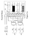
- FIGS. 3 - a and 3 - b show the control flow of the proposed method working in parallel mode and sequential mode, respectively. These figures are used to describe how to perform buffer transfer.
- the proposed control signal circuit consists of the following parts: a transfer mode control signal circuit 300 , a data access circuit in parallel mode ( 400 and 450 ), and a data access circuit in sequential mode (comprising data read control signal circuits 400 and 510 , and data write control signal circuit 550 and 560 ).
- a transfer mode control signal circuit 300 in parallel mode, the transfer mode control signal circuit activates the data access circuit in parallel mode and performs parallel data accessing.
- the transfer mode control signal circuit activates the data access circuit in sequential mode and performs data accessing sequentially.
- each control signal contains an (m+n)-bit binary number, where the most significant m bits indicate a block and the other n bits indicate a register in the block.
- FIGS. 4 - a and 4 - b are used to describe the association between the control signal circuit and the memory.
- each control signal contains an (m+n)-bit binary number, where the most significant m bits 600 indicate a block and the other n bits 700 indicate a register in the block.
- the memory must have 2 m memory blocks, and each block must have 2 n registers (as shown in FIG. 4 - a ).
- FIG. 1 - a shows the control flow of the prior circuit design in parallel mode.
- FIG. 1 - b shows the control flow of the prior circuit design in sequential mode.
- FIG. 2 shows the control flow of the proposed method.
- FIG. 3 - a shows an execution scenario of the proposed method in parallel mode.
- FIG. 3 - b shows an execution scenario of the proposed method in sequential mode.
- FIGS. 4 - a and 4 - b show the association between the proposed control signal circuit and the memory block.
Landscapes
- Engineering & Computer Science (AREA)
- Computer Hardware Design (AREA)
- Physics & Mathematics (AREA)
- Theoretical Computer Science (AREA)
- Evolutionary Computation (AREA)
- Geometry (AREA)
- General Engineering & Computer Science (AREA)
- General Physics & Mathematics (AREA)
- Information Transfer Systems (AREA)
Abstract
Description
Claims (10)
Priority Applications (1)
| Application Number | Priority Date | Filing Date | Title |
|---|---|---|---|
| US10/626,736 US6971075B2 (en) | 2003-07-25 | 2003-07-25 | Circuit design method to control access pointers of different memory |
Applications Claiming Priority (1)
| Application Number | Priority Date | Filing Date | Title |
|---|---|---|---|
| US10/626,736 US6971075B2 (en) | 2003-07-25 | 2003-07-25 | Circuit design method to control access pointers of different memory |
Publications (2)
| Publication Number | Publication Date |
|---|---|
| US20050018491A1 US20050018491A1 (en) | 2005-01-27 |
| US6971075B2 true US6971075B2 (en) | 2005-11-29 |
Family
ID=34080472
Family Applications (1)
| Application Number | Title | Priority Date | Filing Date |
|---|---|---|---|
| US10/626,736 Expired - Fee Related US6971075B2 (en) | 2003-07-25 | 2003-07-25 | Circuit design method to control access pointers of different memory |
Country Status (1)
| Country | Link |
|---|---|
| US (1) | US6971075B2 (en) |
Citations (3)
| Publication number | Priority date | Publication date | Assignee | Title |
|---|---|---|---|---|
| US6009245A (en) * | 1997-03-13 | 1999-12-28 | Seiko Epson Corporation | Serial printer, and image buffer access method for serial printer |
| US6499083B1 (en) * | 1999-09-15 | 2002-12-24 | Western Digital Ventures, Inc. | Disk-based storage system responsive to a direction-selection signal for autonomously controlling seeks in a sequence determined by the direction-selection signal and a locally-stored doubly linked list |
| US20040085982A1 (en) * | 2002-10-07 | 2004-05-06 | Lg Electronics Inc. | Apparatus and method for queue assignment for each link in multi-links of an access pointer controller |
-
2003
- 2003-07-25 US US10/626,736 patent/US6971075B2/en not_active Expired - Fee Related
Patent Citations (3)
| Publication number | Priority date | Publication date | Assignee | Title |
|---|---|---|---|---|
| US6009245A (en) * | 1997-03-13 | 1999-12-28 | Seiko Epson Corporation | Serial printer, and image buffer access method for serial printer |
| US6499083B1 (en) * | 1999-09-15 | 2002-12-24 | Western Digital Ventures, Inc. | Disk-based storage system responsive to a direction-selection signal for autonomously controlling seeks in a sequence determined by the direction-selection signal and a locally-stored doubly linked list |
| US20040085982A1 (en) * | 2002-10-07 | 2004-05-06 | Lg Electronics Inc. | Apparatus and method for queue assignment for each link in multi-links of an access pointer controller |
Also Published As
| Publication number | Publication date |
|---|---|
| US20050018491A1 (en) | 2005-01-27 |
Similar Documents
| Publication | Publication Date | Title |
|---|---|---|
| US11074190B2 (en) | Slot/sub-slot prefetch architecture for multiple memory requestors | |
| US6078977A (en) | Hierarchical bus structure access system | |
| US5075846A (en) | Memory access serialization as an MMU page attribute | |
| CN104520817B (en) | Apparatus and method for emulating a multi-port memory | |
| US8601229B2 (en) | Secure memory access system and method | |
| CN114860329A (en) | Dynamic consistency biasing configuration engine and method | |
| US9710191B1 (en) | Rapid memory buffer write storage system and method | |
| WO1999041670A1 (en) | System for dynamically changing draining priority of a receive fifo | |
| US7343469B1 (en) | Remapping I/O device addresses into high memory using GART | |
| US9098425B2 (en) | Implementing user mode foreign device attachment to memory channel | |
| US7844752B2 (en) | Method, apparatus and program storage device for enabling multiple asynchronous direct memory access task executions | |
| CN112988647A (en) | TileLink bus-to-AXI 4 bus conversion system and method | |
| US6336158B1 (en) | Memory based I/O decode arrangement, and system and method using the same | |
| TW440761B (en) | The cache device and method | |
| US6971075B2 (en) | Circuit design method to control access pointers of different memory | |
| KR100463205B1 (en) | Computer system embedded sequantial buffer for improving DSP data access performance and data access method thereof | |
| CN110187919B (en) | Device, method and system for configuring register | |
| EP0690382A2 (en) | Computer system with a multiplexed address bus and pipelined write operations | |
| US6801988B2 (en) | Data buffer for block unit data transfer to SDRAM | |
| CN112000592B (en) | Method and device for data interaction between modules | |
| US6134609A (en) | Method for using computer system memory as a modem data buffer by transferring modem I/O data directly to system controller and transferring corresponding system controller data directly to main memory | |
| US12124388B2 (en) | Bridge control chip and associated signal processing method | |
| CN120164500B (en) | Controller circuit for solving ADC conversion data loss | |
| US20260037435A1 (en) | NVMe SSD AND STORAGE SYSTEM INCLUDING THE SAME | |
| KR20050004997A (en) | Data transmission handling apparatus |
Legal Events
| Date | Code | Title | Description |
|---|---|---|---|
| AS | Assignment |
Owner name: DESTINY TECHNOLOGY CORPORATION, TAIWAN Free format text: ASSIGNMENT OF ASSIGNORS INTEREST;ASSIGNOR:LIN, CHE-SHENG;REEL/FRAME:014330/0489 Effective date: 20030410 |
|
| AS | Assignment |
Owner name: PIRMAX ELECTRONICS LTD.,TAIWAN Free format text: MERGER;ASSIGNOR:DESTINY TECHNOLOGY CORPORATION;REEL/FRAME:018284/0100 Effective date: 20060920 Owner name: PIRMAX ELECTRONICS LTD., TAIWAN Free format text: MERGER;ASSIGNOR:DESTINY TECHNOLOGY CORPORATION;REEL/FRAME:018284/0100 Effective date: 20060920 |
|
| AS | Assignment |
Owner name: PRIMAX ELECTRONICS LTD., TAIWAN Free format text: CORRECTIVE ASSIGNMENT TO CORRECT THE ASSIGNEE'S NAME PREVIOUSLY RECORDED ON REEL 018284 FRAME 0100;ASSIGNOR:DESTINY TECHNOLOGY CORPORATION;REEL/FRAME:018431/0220 Effective date: 20060902 Owner name: PRIMAX ELECTRONICS LTD.,TAIWAN Free format text: CORRECTIVE ASSIGNMENT TO CORRECT THE ASSIGNEE'S NAME PREVIOUSLY RECORDED ON REEL 018284 FRAME 0100;ASSIGNOR:DESTINY TECHNOLOGY CORPORATION;REEL/FRAME:018431/0220 Effective date: 20060902 |
|
| FEPP | Fee payment procedure |
Free format text: PAT HOLDER NO LONGER CLAIMS SMALL ENTITY STATUS, ENTITY STATUS SET TO UNDISCOUNTED (ORIGINAL EVENT CODE: STOL); ENTITY STATUS OF PATENT OWNER: LARGE ENTITY |
|
| REFU | Refund |
Free format text: REFUND - PAYMENT OF MAINTENANCE FEE, 4TH YEAR, LARGE ENTITY (ORIGINAL EVENT CODE: R1551); ENTITY STATUS OF PATENT OWNER: LARGE ENTITY |
|
| FPAY | Fee payment |
Year of fee payment: 4 |
|
| FPAY | Fee payment |
Year of fee payment: 8 |
|
| REMI | Maintenance fee reminder mailed | ||
| LAPS | Lapse for failure to pay maintenance fees |
Free format text: PATENT EXPIRED FOR FAILURE TO PAY MAINTENANCE FEES (ORIGINAL EVENT CODE: EXP.) |
|
| STCH | Information on status: patent discontinuation |
Free format text: PATENT EXPIRED DUE TO NONPAYMENT OF MAINTENANCE FEES UNDER 37 CFR 1.362 |
|
| FP | Lapsed due to failure to pay maintenance fee |
Effective date: 20171129 |