US6956945B2 - Method and apparatus for phantom battery feed - Google Patents
Method and apparatus for phantom battery feed Download PDFInfo
- Publication number
- US6956945B2 US6956945B2 US10/384,300 US38430003A US6956945B2 US 6956945 B2 US6956945 B2 US 6956945B2 US 38430003 A US38430003 A US 38430003A US 6956945 B2 US6956945 B2 US 6956945B2
- Authority
- US
- United States
- Prior art keywords
- amplifier
- voltage
- supply terminal
- supply
- negative
- Prior art date
- Legal status (The legal status is an assumption and is not a legal conclusion. Google has not performed a legal analysis and makes no representation as to the accuracy of the status listed.)
- Expired - Lifetime, expires
Links
Images


Classifications
-
- H—ELECTRICITY
- H04—ELECTRIC COMMUNICATION TECHNIQUE
- H04L—TRANSMISSION OF DIGITAL INFORMATION, e.g. TELEGRAPHIC COMMUNICATION
- H04L25/00—Baseband systems
- H04L25/02—Details ; arrangements for supplying electrical power along data transmission lines
-
- H—ELECTRICITY
- H04—ELECTRIC COMMUNICATION TECHNIQUE
- H04M—TELEPHONIC COMMUNICATION
- H04M19/00—Current supply arrangements for telephone systems
-
- Y—GENERAL TAGGING OF NEW TECHNOLOGICAL DEVELOPMENTS; GENERAL TAGGING OF CROSS-SECTIONAL TECHNOLOGIES SPANNING OVER SEVERAL SECTIONS OF THE IPC; TECHNICAL SUBJECTS COVERED BY FORMER USPC CROSS-REFERENCE ART COLLECTIONS [XRACs] AND DIGESTS
- Y02—TECHNOLOGIES OR APPLICATIONS FOR MITIGATION OR ADAPTATION AGAINST CLIMATE CHANGE
- Y02D—CLIMATE CHANGE MITIGATION TECHNOLOGIES IN INFORMATION AND COMMUNICATION TECHNOLOGIES [ICT], I.E. INFORMATION AND COMMUNICATION TECHNOLOGIES AIMING AT THE REDUCTION OF THEIR OWN ENERGY USE
- Y02D30/00—Reducing energy consumption in communication networks
- Y02D30/70—Reducing energy consumption in communication networks in wireless communication networks
Definitions
- This invention relates generally to telecommunications, and, more particularly, to providing a phantom battery feed for power savings in amplifier circuits.
- a line card generally connects the subscriber station to the central switching office.
- the functions of the line card include supplying talk battery, performing wake-up sequences of circuits to allow communications to take place, and the like.
- Voltage signals are processed and conditioned when being driven onto telecommunication lines.
- POTS was designed primarily for voice communication, and thus provides an inadequate data transmission rate for many modern applications.
- designers have sought innovative and cost-effective solutions that would take advantage of the existing network infrastructure.
- Several technological solutions proposed in the telecommunications industry use the existing network of telephone wires.
- a promising one of these technologies is the Digital Subscriber Line (xDSL or DSL) technology.
- xDSL is making the existing network of telephone lines more robust and versatile. Once considered virtually unusable for broadband communications, an ordinary twisted pair equipped with DSL interfaces can transmit video, television, and very high-speed data. The fact that more than six hundred million telephone lines exist around the world is a compelling reason for these lines to be used as the primary transmission conduits for at least several more decades. Because DSL utilizes telephone wiring already installed in virtually every home and business in the world, it has been embraced by many as one of the more promising and viable options.
- DSL Digital Subscriber Line
- VDSL Very High-Speed Digital Subscriber Line
- SDSL Symmetric Digital Subscriber Line
- DSL and POTS technologies can co-exist in one line (e.g., also referred to as a “subscriber line”).
- Traditional analog voice band interfaces use the same frequency band, 0-4 Kilohertz (KHz), as telephone service, thereby preventing concurrent voice and data use.
- KHz Kilohertz
- a DSL interface operates at frequencies above the voice channels, from 25 KHz to 1.1 Megahertz (MHz).
- MHz Megahertz
- DSL systems use digital signal processing (DSP) to increase throughput and signal quality through common copper telephone wire. It provides a downstream data transfer rate from the DSL Point-of-Presence (POP) to the subscriber location at speeds of up to 1.5 mega-bits per second (MBPS).
- POP Point-of-Presence
- MBPS mega-bits per second
- DSL systems generally employ a signal detection system that monitors the telephone line for communication requests. More specifically, the line card in the central office polls the telephone line to detect any communication requests from a DSL data transceiver, such as a DSL modem, located at a subscriber station.
- a DSL data transceiver such as a DSL modem
- the additional resources required to deal with excessive power consumption can cause signal problems in communications signals. More resources, such as more circuit elements, can cause noise and distortion in signals that are processed by the line card. Integrity of voice and/or data signals can be compromised, causing communications data corruption. Remote line card systems may require additional resources, such as more portable power supplies and related circuitry. Therefore, excessive power consumption can cause appreciable inefficiencies in the operation of line cards and the communication system as a whole.
- the present invention is directed to overcoming, or at least reducing the effects of, one or more of the problems set forth above.
- a method for a performing a phantom battery feed into a circuit.
- a voltage signal is driven onto a telecommunications line using a first amplifier and a second amplifier.
- a phantom battery feed is performed during a negative cycle of the voltage signal.
- Performing the phantom battery feed comprises: supplying a negative supply terminal of the first amplifier with a supply voltage that is one-half of a full scale supply voltage; and supplying a positive supply terminal of the second amplifier with a supply voltage that is one-half of the full scale supply voltage.
- an apparatus for performing a phantom battery feed into a circuit.
- the apparatus of the present invention comprises: a first amplifier comprising a positive supply terminal and a negative supply terminal; a first switch coupled with said negative supply terminal of said first amplifier, said switch being adapted to transition said negative supply terminal from a full scale voltage source to a half scale voltage source; a second amplifier comprising a positive supply terminal and a negative supply terminal; and a second switch coupled with said positive supply terminal of said second amplifier, said switch being adapted to transition said positive supply terminal from a full scale voltage source to a half scale voltage source.
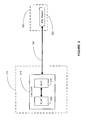
- FIG. 1 illustrates a first embodiment of an apparatus in accordance with the present invention
- FIG. 2 illustrates an implementation of a line card into the apparatus described in FIG. 1 ;
- FIG. 3 illustrates a more detailed depiction of the line card in accordance with one embodiment of the present invention
- FIG. 4 illustrates a more detailed depiction of the SLIC, described in FIG. 3 , in accordance with one embodiment of the present invention
- FIG. 5 illustrates a more detailed depiction of the SLIC, which comprises a circuit capable of conditioning a communications signal
- FIG. 6 depicts a graph that illustrates the communications signal that is conditioned by the circuit described in FIG. 6 ;
- FIG. 7 illustrates a more detailed depiction of the SLIC which comprises a circuit that contains a phantom battery feed in accordance with one embodiment of the present invention, which is used to condition the communication signal described in FIG. 5 ;
- FIG. 8 illustrates one embodiment of a voltage supply utilized by the circuit described in FIG. 7 .
- Embodiments of the present invention provide for a method and apparatus for reducing power consumption in an amplifier circuit used to condition a communications signal. Embodiments of the present invention also provide for employing a phantom battery feed to reduce power consumption in a circuit. Embodiments of the present invention provide for reducing power consumption in a differential amplifier circuit.
- the apparatus 100 includes a central office 110 that is coupled a subscriber station 120 via a subscriber line 130 .
- the central office 110 and the subscriber station 120 are capable of sending and receiving a signal comprising voice and data band.
- the voice band refers to a POTS voice signal ranging from 0-4 KHz.
- the data band refers to frequencies above the voice band, and may include, for example, the frequency range employed in xDSL technologies.
- the subscriber line 130 may be a Public Switched Telephone Network (PSTN) line, a Private Branch Exchange (PBX) line, or any other medium capable of transmitting signals.
- PSTN Public Switched Telephone Network
- PBX Private Branch Exchange
- the subscriber station 120 may be a telephonic device capable of supporting pulse dialing.
- the subscriber station 120 may be one of a variety of available conventional telephones, such as wired telephones and similar devices.
- the subscriber station 120 may be any “device” capable of performing a substantially equivalent function of a conventional telephone, which may include, but is not limited to, transmitting and/or receiving voice and data signals.
- Examples of the subscriber station 120 include a data processing system (DPS) utilizing a modem to perform telephony, a television phone, a wireless local loop, a DPS working in conjunction with a telephone, Internet Protocol (IP) telephony, and the like.
- IP telephony is a general term for the technologies that use the Internet Protocol's packet-switched connections to exchange voice, fax, and other forms of information that have traditionally been carried over the dedicated circuit-switched connections of the public switched telephone network (PSTN).
- PSTN public switched telephone network
- IP telephony is an Internet Phone, a software program that runs on a DPS and simulates a conventional phone, allowing an end user to speak through a microphone and hear through DPS speakers. The calls travel over the Internet as packets of data on shared lines, avoiding the tolls of the PSTN.
- a line card 210 and a DSL modem 220 are illustrated in accordance with the present invention.
- the line card 210 which is integrated into the central office 110 , is coupled with the DSL modem 220 , which resides within the subscriber station 120 . Because voice and/or data can be transmitted on the subscriber line 130 , the signal received and transmitted by the line card 210 and the DSL modem 220 may include voice and data band frequencies.
- the line card 210 may be located at a central office or a remote location somewhere between the central office and the subscriber station 120 (see FIG. 1 ).
- the line card 210 services the subscriber station 120 , which in the illustrated embodiment is a telephonic device.
- the line card 210 is capable of processing DC voltage signals and AC signals.
- the subscriber line 130 in the instant embodiment is a telephone line.
- the combination of the telephone device 120 and the telephone line 130 is generally referred to as a subscriber loop.
- the line card 210 which may be capable of supporting a plurality of subscriber lines 130 , performs, among other things, two fundamental functions: DC loop supervision and DC feed.
- the purpose of DC feed is to supply enough power to operate the telephone device 120 at the customer end.
- the purpose of DC loop supervision is to detect changes in DC load, such as on-hook events, off-hook events, rotary dialing, or any other event that causes the DC load to change. In the interest of clarity and to avoid obscuring the invention, only that portion of the line card 210 that is helpful to the understanding of the invention is illustrated.
- the line driver 210 comprises a subscriber line interface circuit (SLIC) 310 as well as a subscriber line audio-processing circuit (SLAC) 320 .
- the SLIC 310 performs a variety of interface functions between the line driver 210 and the subscriber line 130 .
- the SLIC 310 is also capable of performing a variety of functions, such as battery feed, overload protection, polarity reversal, on-hook transmission, and current limiting.
- the SLIC 310 is connected to the SLAC 320 .
- the SLAC 320 is capable of processing analog-to-digital (A/D) and digital-to-analog (D/A) signal conversion, filtering, feed control, and supervision.
- A/D analog-to-digital
- D/A digital-to-analog
- the phantom battery feed disclosed by embodiments of the present invention is provided in the SLIC 310 .
- the SLIC 310 comprises a differential amplifier circuit, which is a circuit that is characterized by phantom battery feed circuit 410 .
- the phantom battery feed circuit 410 is capable of reducing power consumption in a circuit that conditions a communication signal.
- the phantom battery feed circuit 410 is capable of reducing power consumption during certain portions of a signal cycle.
- the circuit 500 comprises a differential amplifier circuit that is capable of conditioning a differential communication voltage signal 580 .
- the circuit 500 shown in FIG. 5 comprises an amplifier-A 510 , an amplifier-B 520 , an equivalent circuit capacitance (C) 530 , and an equivalent circuit resistance (R) 540 .
- the circuit shown in FIG. 5 conditions the differential communications voltage signal 580 , such that the voltage signal 580 can be driven on the subscriber line 130 .
- the amplifier A 510 operates between the voltage-level defined by ground (GND) and a minus battery voltage ( ⁇ BATT).
- the amplifier B 520 operates between GND and ⁇ BATT.
- FIG. 6 two cycles of the voltage signal 580 are illustrated.
- the voltage signal 580 experiences a positive cycle 610 and a negative cycle 620 .
- Current in the circuit 500 flows in one direction during the positive cycle 610 of the voltage signal 580 , and in the opposite direction during the negative cycle 620 of the voltage signal.
- an AC current (I AC — 1 ) 560 is induced.
- an AC current (I AC2 ) 570 is induced.
- sample voltage, current, and battery values are used.
- teachings of the present invention can be used for a variety of voltage, current, and battery values by those skilled in the art who have the benefit of the present disclosure.
- the concept of a phantom battery feed taught by embodiments of the present invention is generally implemented when a DC offset between the amplifiers 510 and 520 that is greater than the AC swing of the voltage signal 580 is present.
- the DC offset between the amplifiers 510 and 520 is typically greater than the AC swings of the voltage signal 580 .
- Circuit overhead in the line card 210 generally calls for approximately another 6 volts. Therefore, in one embodiment, the operational range of the amplifiers 510 , 520 is set from ground (GND) to ⁇ 82 volts ( ⁇ BATT).
- the amplifier-A 510 will be biased at ⁇ 21 volts and the amplifier-B 520 will be biased at ⁇ 61 volts.
- the average battery current is approximately equal to the average AC current (I AC — 1 560 and I AC — 2 570 ), which is approximately 31.6 milliamps plus the idle current of the line card 210 (7 milliamps) for a total current of approximately 38.6 milliamps. Therefore, the power dissipated in the load (C 530 and R 540 ) is approximately 170 milliwatts, thus, the remaining power (approximately 3 Watts), which can be excessive, is dissipated in the line card 210 .
- the power dissipation of the amplifier-A 510 is approximately 21 volts (i.e., the difference between the amplifier-A 510 output signal and the positive supply) multiplied by the AC current, I AC — 1 560 .
- the power dissipation of the amplifier-B 520 output signal is approximately 21 volts (i.e., the difference between the amplifier-B 520 output and the negative supply) multiplied by the AC current, I AC — 1 560 . Since the positive cycle 610 is half of the entire period of the voltage signal 580 , the power dissipation calculations of the positive cycle 610 is valid for 50% of the operation time. During this half cycle (i.e., the positive cycle 610 ), the power dissipated in the amplifiers 510 , 520 is approximately 42 volts multiplied by the value of the AC current, I AC — 1 560 .
- the power dissipation of the amplifier-A 510 is approximately 61 volts (i.e., the difference between the amplifier-A 520 output signal and the negative supply) multiplied by the AC current, I AC — 2 570 .
- the power dissipation of the amplifier-B 520 is approximately 61 volts (i.e., the difference between the amplifier-B 520 output signal and the positive supply) multiplied by the AC current, I AC — 2 570 .
- the circuit 700 comprises the amplifier-A 510 , the amplifier-B 520 , the capacitor C 530 , the resistor R 540 , a switch-A 710 , a switch-B 720 , a voltage source 730 , and a switch control unit 750 .
- the switches 710 , 720 are connected to the voltage source 730 , which can provide a voltage level of one-half the value of BATT ( ⁇ BATT/2) on a line 740 .
- the voltage source 730 is a voltage regulator illustrated in FIG. 8 .
- the phantom battery feed circuit 700 provides a “phantom” battery (i.e., the voltage source 730 ) equal to ⁇ BATT/2, which is approximately equal to ⁇ 41 volts in the illustrative example described above.
- the negative supply of the amplifier-A 520 can be switched between ⁇ BATT and the output signal of the phantom battery (on the line 740 ), which has a voltage of ⁇ BATT/2.
- the switch 720 the positive supply of the amplifier-B 520 can be switched between GND and ⁇ BATT/2.
- the switch control unit 750 can be used to control movement of the switches 710 , 720 , which allows for switching the amplifier supplies for improving efficiency.
- the switches 710 and 720 are activated to position 1 (i.e., normal operation).
- the switches 710 and 720 are activated to position 2 (i.e., phantom battery feed operation), which results in power savings.
- the phantom battery When the switches 710 , 720 are activated to position 2 , the phantom battery replaces ⁇ BATT as the negative supply for the amplifier-A 510 .
- the phantom battery also replaces GND as the positive supply for the amplifier-B 520 . Since the operational voltages of the amplifiers 510 , 520 are generally 20 volts away from their DC bias point, and the fact that only a 17 volt swing exists, the phantom battery provides adequate swing for each of the amplifiers 510 and 520 .
- the switches 710 , 720 are activated into position 1 and the analysis of the circuit 700 is similar to the analysis of the circuit 500 , which is described above.
- the power dissipated during the positive cycle 610 is approximately 42 volts multiplied by the AC current, I AC — 1 (again multiplied by 50%, or 21*I AC — 1 ).
- the switches 710 , 720 are activated to position 2 , invoking the phantom battery operation mode.
- the power dissipated in the amplifier-A 510 is 21 volts multiplied by I AC — 2 since the negative supply is now ⁇ 41V.
- the power dissipated in the amplifier-B 520 is 21 volts multiplied by I AC — 2 since the positive supply is also ⁇ 41V.
- the total power dissipated during the negative cycle 620 is [(42 volts)*I AC — 2 *50%] (i.e., 21*I AC — 2 ). Therefore, the total power dissipated in the operation of the circuit 700 during the negative cycle 620 is [(21*I AC — 1 )+(21*I AC — 2 )]
- the battery current during the positive cycle 610 is I AC — 1 .
- the switches are activated to position 2 , invoking the phantom battery operation mode.
- the positive supply of amplifier-B 520 and the negative supply of the amplifier-A 510 are both ⁇ BATT/2, or ⁇ 41 volts, therefore, the I AC — 2 570 is approximately zero.
- the total power dissipated during the operation of the circuit 700 during the negative cycle 620 is [(21*I AC — 2 )+(21*I AC — 2 )], but I AC — 2 is now zero, therefore, the total power dissipation during the negative cycle is simply 21*I AC — 1 . Furthermore, I AC — 1 does not exist, as defined in FIG. 7 , during the negative cycle 620 , thus the total power dissipation during the negative cycle 620 is approximately zero.
- the power dissipation during the operation of the circuit 700 is half of the power dissipation for the same period in circuit 500 .
- each amplifier 710 , 720 draws equal and opposite currents from the phantom battery, therefore, there is virtually zero current flow in or out of the phantom supply. In reality, some idling current from the amplifiers 710 , 720 will flow in the phantom battery, however that current would have flowed through the ⁇ BATT power supply.
- the phantom battery effectively re-uses current during the negative half cycles due to the DC offset. The current reversals are overcome by the DC offset and capacitance of the line.
- the phantom battery feed apparatus and method illustrated in the present invention can be used in a variety of electronic circuitry by those skilled in the art.
- the concepts taught by embodiments of the present invention can be utilized in a variety of electronic applications.
- the apparatuses 110 , 120 , 130 can be integrated in a system capable of transmitting and receiving signals having a voice band and a data band.
- the teachings of the present invention may be implemented in a line card 210 that supports both POTS and ADSL technologies.
Landscapes
- Engineering & Computer Science (AREA)
- Signal Processing (AREA)
- Power Engineering (AREA)
- Computer Networks & Wireless Communication (AREA)
- Interface Circuits In Exchanges (AREA)
- Telephone Function (AREA)
Abstract
Description
Claims (26)
Priority Applications (1)
| Application Number | Priority Date | Filing Date | Title |
|---|---|---|---|
| US10/384,300 US6956945B2 (en) | 2003-03-07 | 2003-03-07 | Method and apparatus for phantom battery feed |
Applications Claiming Priority (1)
| Application Number | Priority Date | Filing Date | Title |
|---|---|---|---|
| US10/384,300 US6956945B2 (en) | 2003-03-07 | 2003-03-07 | Method and apparatus for phantom battery feed |
Publications (2)
| Publication Number | Publication Date |
|---|---|
| US20040174993A1 US20040174993A1 (en) | 2004-09-09 |
| US6956945B2 true US6956945B2 (en) | 2005-10-18 |
Family
ID=32927236
Family Applications (1)
| Application Number | Title | Priority Date | Filing Date |
|---|---|---|---|
| US10/384,300 Expired - Lifetime US6956945B2 (en) | 2003-03-07 | 2003-03-07 | Method and apparatus for phantom battery feed |
Country Status (1)
| Country | Link |
|---|---|
| US (1) | US6956945B2 (en) |
Cited By (5)
| Publication number | Priority date | Publication date | Assignee | Title |
|---|---|---|---|---|
| US20070291930A1 (en) * | 2006-06-15 | 2007-12-20 | Apfel Russell J | Output stacking architecture for an amplifier |
| US20070291929A1 (en) * | 2006-06-15 | 2007-12-20 | Apfel Russell J | Methods and apparatus for performing subscriber line interface functions |
| US20070290739A1 (en) * | 2006-06-15 | 2007-12-20 | Apfel Russell J | Current mirror architectures |
| US20080159525A1 (en) * | 2006-12-27 | 2008-07-03 | Apfel Russell J | Tracking voltage regulator for a subscriber line interface circuit |
| US20080159487A1 (en) * | 2006-12-27 | 2008-07-03 | Apfel Russell J | Methods and apparatus for low voltage control of a subscriber line interface circuit |
Families Citing this family (3)
| Publication number | Priority date | Publication date | Assignee | Title |
|---|---|---|---|---|
| DE102005005538B4 (en) * | 2005-02-07 | 2007-04-05 | Infineon Technologies Ag | Line driver circuit with high efficiency |
| US7801293B2 (en) | 2005-11-10 | 2010-09-21 | Alcatel-Lucent Usa Inc. | Ringback tone preference information to assist selection of ringback tone |
| US7411431B2 (en) * | 2006-02-06 | 2008-08-12 | Fairchild Semiconductor Corporation | Dual output differential line driver using single current |
Citations (1)
| Publication number | Priority date | Publication date | Assignee | Title |
|---|---|---|---|---|
| US6233335B1 (en) * | 1998-05-15 | 2001-05-15 | Intersil Corporation | Battery switching subscriber loop interface circuit |
-
2003
- 2003-03-07 US US10/384,300 patent/US6956945B2/en not_active Expired - Lifetime
Patent Citations (1)
| Publication number | Priority date | Publication date | Assignee | Title |
|---|---|---|---|---|
| US6233335B1 (en) * | 1998-05-15 | 2001-05-15 | Intersil Corporation | Battery switching subscriber loop interface circuit |
Cited By (9)
| Publication number | Priority date | Publication date | Assignee | Title |
|---|---|---|---|---|
| US20070291930A1 (en) * | 2006-06-15 | 2007-12-20 | Apfel Russell J | Output stacking architecture for an amplifier |
| US20070291929A1 (en) * | 2006-06-15 | 2007-12-20 | Apfel Russell J | Methods and apparatus for performing subscriber line interface functions |
| US20070290739A1 (en) * | 2006-06-15 | 2007-12-20 | Apfel Russell J | Current mirror architectures |
| US7477095B2 (en) | 2006-06-15 | 2009-01-13 | Silicon Laboratories Inc. | Current mirror architectures |
| US7970125B2 (en) | 2006-06-15 | 2011-06-28 | Silicon Laboratories Inc. | Output stacking architecture for an amplifier |
| US20080159525A1 (en) * | 2006-12-27 | 2008-07-03 | Apfel Russell J | Tracking voltage regulator for a subscriber line interface circuit |
| US20080159487A1 (en) * | 2006-12-27 | 2008-07-03 | Apfel Russell J | Methods and apparatus for low voltage control of a subscriber line interface circuit |
| US8019077B2 (en) | 2006-12-27 | 2011-09-13 | Silicon Laboratories Inc. | Methods and apparatus for low voltage control of a subscriber line interface circuit |
| US8249247B2 (en) | 2006-12-27 | 2012-08-21 | Silicon Laboratories Inc. | Tracking voltage regulator for a subscriber line interface circuit |
Also Published As
| Publication number | Publication date |
|---|---|
| US20040174993A1 (en) | 2004-09-09 |
Similar Documents
| Publication | Publication Date | Title |
|---|---|---|
| US6522730B1 (en) | DSL communication system with improved bandwidth | |
| US6647117B1 (en) | Continuity of voice carried over DSL during power failure | |
| US6295343B1 (en) | Method and apparatus for combining voice line card and xDSL line card functions | |
| US20110019725A1 (en) | Dsl method having variable upload/download bit rate and application-specific dynamic profile switching | |
| US6674845B2 (en) | Method and apparatus for connecting broadband voice and data signals to telephone systems | |
| JP3760073B2 (en) | System and method for assigning overhead voltage in transmission of POTS and XDSL signals | |
| US20050073995A1 (en) | Voice-over-internet protocol device | |
| US8594078B2 (en) | Method and apparatus for stand-alone voice over internet protocol with POTS telephone support | |
| US6956945B2 (en) | Method and apparatus for phantom battery feed | |
| US7113590B2 (en) | Method and apparatus for a differential feedback in an active impedence feedback circuit | |
| US6922415B1 (en) | Apparatus and method for a non-symmetrical half-duplex DSL modem | |
| US6690768B2 (en) | Power cutback configuration of digital subscriber line transceivers using public switched telephone network signaling | |
| US7181002B2 (en) | Method and apparatus for a single power supply for dual power mode | |
| US7254229B2 (en) | Method and apparatus for an active impedance feedback | |
| US6778663B1 (en) | Method and apparatus for sensing current | |
| US7260210B2 (en) | Unbalanced slic with a built-in ring circuit | |
| US20020106072A1 (en) | Method and apparatus for improving gain bandwidth paths | |
| US7453896B1 (en) | Method and apparatus for longitudinal balance calibration | |
| US6628534B2 (en) | Method and apparatus for improving voltage to current signal conversion | |
| KR100359476B1 (en) | Internal ADSL modem which support voice over Internet Protocol with legacy telephone | |
| US7027590B2 (en) | Dynamic allocation of overhead voltage to support simultaneous transmission of signals on a telecommunication line | |
| CN1222147C (en) | Voice over Internet protocol device | |
| US20080118058A1 (en) | Splitter with Active Transient Suppression Circuit | |
| JP4197636B2 (en) | DSL communication method and apparatus | |
| US8090095B2 (en) | Method and apparatus for power-mode control |
Legal Events
| Date | Code | Title | Description |
|---|---|---|---|
| AS | Assignment |
Owner name: LEGERITY, INC., TEXAS Free format text: ASSIGNMENT OF ASSIGNORS INTEREST;ASSIGNOR:APFEL, RUSSELL J.;REEL/FRAME:013873/0504 Effective date: 20030304 |
|
| STCF | Information on status: patent grant |
Free format text: PATENTED CASE |
|
| CC | Certificate of correction | ||
| AS | Assignment |
Owner name: LEGERITY, INC., TEXAS Free format text: RELEASE BY SECURED PARTY;ASSIGNOR:MORGAN STANLEY SENIOR FUNDING INC;REEL/FRAME:019640/0676 Effective date: 20070803 Owner name: LEGERITY, INC.,TEXAS Free format text: RELEASE BY SECURED PARTY;ASSIGNOR:MORGAN STANLEY SENIOR FUNDING INC;REEL/FRAME:019640/0676 Effective date: 20070803 |
|
| FPAY | Fee payment |
Year of fee payment: 4 |
|
| FPAY | Fee payment |
Year of fee payment: 8 |
|
| AS | Assignment |
Owner name: ZARLINK SEMICONDUCTOR (U.S.) INC., TEXAS Free format text: MERGER;ASSIGNOR:LEGERITY, INC.;REEL/FRAME:031746/0171 Effective date: 20071130 Owner name: MICROSEMI SEMICONDUCTOR (U.S.) INC., TEXAS Free format text: CHANGE OF NAME;ASSIGNOR:ZARLINK SEMICONDUCTOR (U.S.) INC.;REEL/FRAME:031746/0214 Effective date: 20111121 |
|
| AS | Assignment |
Owner name: MORGAN STANLEY & CO. LLC, NEW YORK Free format text: PATENT SECURITY AGREEMENT;ASSIGNOR:MICROSEMI SEMICONDUCTOR (U.S.) INC.;REEL/FRAME:031729/0667 Effective date: 20131125 |
|
| AS | Assignment |
Owner name: BANK OF AMERICA, N.A., AS SUCCESSOR AGENT, NORTH C Free format text: NOTICE OF SUCCESSION OF AGENCY;ASSIGNOR:ROYAL BANK OF CANADA (AS SUCCESSOR TO MORGAN STANLEY & CO. LLC);REEL/FRAME:035657/0223 Effective date: 20150402 |
|
| AS | Assignment |
Owner name: MICROSEMI CORP.-ANALOG MIXED SIGNAL GROUP, A DELAWARE CORPORATION, CALIFORNIA Free format text: RELEASE BY SECURED PARTY;ASSIGNOR:BANK OF AMERICA, N.A.;REEL/FRAME:037558/0711 Effective date: 20160115 Owner name: MICROSEMI SOC CORP., A CALIFORNIA CORPORATION, CALIFORNIA Free format text: RELEASE BY SECURED PARTY;ASSIGNOR:BANK OF AMERICA, N.A.;REEL/FRAME:037558/0711 Effective date: 20160115 Owner name: MICROSEMI SEMICONDUCTOR (U.S.) INC., A DELAWARE CORPORATION, CALIFORNIA Free format text: RELEASE BY SECURED PARTY;ASSIGNOR:BANK OF AMERICA, N.A.;REEL/FRAME:037558/0711 Effective date: 20160115 Owner name: MICROSEMI FREQUENCY AND TIME CORPORATION, A DELAWARE CORPORATION, CALIFORNIA Free format text: RELEASE BY SECURED PARTY;ASSIGNOR:BANK OF AMERICA, N.A.;REEL/FRAME:037558/0711 Effective date: 20160115 Owner name: MICROSEMI COMMUNICATIONS, INC. (F/K/A VITESSE SEMICONDUCTOR CORPORATION), A DELAWARE CORPORATION, CALIFORNIA Free format text: RELEASE BY SECURED PARTY;ASSIGNOR:BANK OF AMERICA, N.A.;REEL/FRAME:037558/0711 Effective date: 20160115 Owner name: MICROSEMI CORP.-MEMORY AND STORAGE SOLUTIONS (F/K/A WHITE ELECTRONIC DESIGNS CORPORATION), AN INDIANA CORPORATION, CALIFORNIA Free format text: RELEASE BY SECURED PARTY;ASSIGNOR:BANK OF AMERICA, N.A.;REEL/FRAME:037558/0711 Effective date: 20160115 Owner name: MICROSEMI SOC CORP., A CALIFORNIA CORPORATION, CAL Free format text: RELEASE BY SECURED PARTY;ASSIGNOR:BANK OF AMERICA, N.A.;REEL/FRAME:037558/0711 Effective date: 20160115 Owner name: MICROSEMI CORP.-ANALOG MIXED SIGNAL GROUP, A DELAW Free format text: RELEASE BY SECURED PARTY;ASSIGNOR:BANK OF AMERICA, N.A.;REEL/FRAME:037558/0711 Effective date: 20160115 Owner name: MICROSEMI SEMICONDUCTOR (U.S.) INC., A DELAWARE CO Free format text: RELEASE BY SECURED PARTY;ASSIGNOR:BANK OF AMERICA, N.A.;REEL/FRAME:037558/0711 Effective date: 20160115 Owner name: MICROSEMI CORP.-MEMORY AND STORAGE SOLUTIONS (F/K/ Free format text: RELEASE BY SECURED PARTY;ASSIGNOR:BANK OF AMERICA, N.A.;REEL/FRAME:037558/0711 Effective date: 20160115 Owner name: MICROSEMI COMMUNICATIONS, INC. (F/K/A VITESSE SEMI Free format text: RELEASE BY SECURED PARTY;ASSIGNOR:BANK OF AMERICA, N.A.;REEL/FRAME:037558/0711 Effective date: 20160115 Owner name: MICROSEMI FREQUENCY AND TIME CORPORATION, A DELAWA Free format text: RELEASE BY SECURED PARTY;ASSIGNOR:BANK OF AMERICA, N.A.;REEL/FRAME:037558/0711 Effective date: 20160115 Owner name: MICROSEMI CORPORATION, CALIFORNIA Free format text: RELEASE BY SECURED PARTY;ASSIGNOR:BANK OF AMERICA, N.A.;REEL/FRAME:037558/0711 Effective date: 20160115 |
|
| AS | Assignment |
Owner name: MORGAN STANLEY SENIOR FUNDING, INC., NEW YORK Free format text: PATENT SECURITY AGREEMENT;ASSIGNORS:MICROSEMI CORPORATION;MICROSEMI SEMICONDUCTOR (U.S.) INC. (F/K/A LEGERITY, INC., ZARLINK SEMICONDUCTOR (V.N.) INC., CENTELLAX, INC., AND ZARLINK SEMICONDUCTOR (U.S.) INC.);MICROSEMI FREQUENCY AND TIME CORPORATION (F/K/A SYMMETRICON, INC.);AND OTHERS;REEL/FRAME:037691/0697 Effective date: 20160115 |
|
| FPAY | Fee payment |
Year of fee payment: 12 |
|
| AS | Assignment |
Owner name: MICROSEMI CORP. - POWER PRODUCTS GROUP, CALIFORNIA Free format text: RELEASE BY SECURED PARTY;ASSIGNOR:MORGAN STANLEY SENIOR FUNDING, INC.;REEL/FRAME:046251/0391 Effective date: 20180529 Owner name: MICROSEMI COMMUNICATIONS, INC., CALIFORNIA Free format text: RELEASE BY SECURED PARTY;ASSIGNOR:MORGAN STANLEY SENIOR FUNDING, INC.;REEL/FRAME:046251/0391 Effective date: 20180529 Owner name: MICROSEMI FREQUENCY AND TIME CORPORATION, CALIFORN Free format text: RELEASE BY SECURED PARTY;ASSIGNOR:MORGAN STANLEY SENIOR FUNDING, INC.;REEL/FRAME:046251/0391 Effective date: 20180529 Owner name: MICROSEMI SEMICONDUCTOR (U.S.), INC., CALIFORNIA Free format text: RELEASE BY SECURED PARTY;ASSIGNOR:MORGAN STANLEY SENIOR FUNDING, INC.;REEL/FRAME:046251/0391 Effective date: 20180529 Owner name: MICROSEMI CORP. - RF INTEGRATED SOLUTIONS, CALIFOR Free format text: RELEASE BY SECURED PARTY;ASSIGNOR:MORGAN STANLEY SENIOR FUNDING, INC.;REEL/FRAME:046251/0391 Effective date: 20180529 Owner name: MICROSEMI CORPORATION, CALIFORNIA Free format text: RELEASE BY SECURED PARTY;ASSIGNOR:MORGAN STANLEY SENIOR FUNDING, INC.;REEL/FRAME:046251/0391 Effective date: 20180529 Owner name: MICROSEMI SOC CORP., CALIFORNIA Free format text: RELEASE BY SECURED PARTY;ASSIGNOR:MORGAN STANLEY SENIOR FUNDING, INC.;REEL/FRAME:046251/0391 Effective date: 20180529 |