US6930362B1 - Calcium doped polysilicon gate electrodes - Google Patents
Calcium doped polysilicon gate electrodes Download PDFInfo
- Publication number
- US6930362B1 US6930362B1 US10/698,167 US69816703A US6930362B1 US 6930362 B1 US6930362 B1 US 6930362B1 US 69816703 A US69816703 A US 69816703A US 6930362 B1 US6930362 B1 US 6930362B1
- Authority
- US
- United States
- Prior art keywords
- polysilicon
- calcium
- layer
- boron
- gate electrode
- Prior art date
- Legal status (The legal status is an assumption and is not a legal conclusion. Google has not performed a legal analysis and makes no representation as to the accuracy of the status listed.)
- Expired - Fee Related
Links
Images


Classifications
-
- H—ELECTRICITY
- H10—SEMICONDUCTOR DEVICES; ELECTRIC SOLID-STATE DEVICES NOT OTHERWISE PROVIDED FOR
- H10D—INORGANIC ELECTRIC SEMICONDUCTOR DEVICES
- H10D64/00—Electrodes of devices having potential barriers
- H10D64/01—Manufacture or treatment
- H10D64/021—Manufacture or treatment using multiple gate spacer layers, e.g. bilayered sidewall spacers
-
- H—ELECTRICITY
- H10—SEMICONDUCTOR DEVICES; ELECTRIC SOLID-STATE DEVICES NOT OTHERWISE PROVIDED FOR
- H10D—INORGANIC ELECTRIC SEMICONDUCTOR DEVICES
- H10D30/00—Field-effect transistors [FET]
- H10D30/60—Insulated-gate field-effect transistors [IGFET]
-
- H—ELECTRICITY
- H10—SEMICONDUCTOR DEVICES; ELECTRIC SOLID-STATE DEVICES NOT OTHERWISE PROVIDED FOR
- H10D—INORGANIC ELECTRIC SEMICONDUCTOR DEVICES
- H10D64/00—Electrodes of devices having potential barriers
- H10D64/01—Manufacture or treatment
- H10D64/013—Manufacture or treatment of electrodes having a conductor capacitively coupled to a semiconductor by an insulator
- H10D64/01302—Manufacture or treatment of electrodes having a conductor capacitively coupled to a semiconductor by an insulator the insulator being formed after the semiconductor body, the semiconductor being silicon
- H10D64/01304—Manufacture or treatment of electrodes having a conductor capacitively coupled to a semiconductor by an insulator the insulator being formed after the semiconductor body, the semiconductor being silicon characterised by the conductor
- H10D64/01306—Manufacture or treatment of electrodes having a conductor capacitively coupled to a semiconductor by an insulator the insulator being formed after the semiconductor body, the semiconductor being silicon characterised by the conductor the conductor comprising a layer of silicon contacting the insulator, e.g. polysilicon
-
- H—ELECTRICITY
- H10—SEMICONDUCTOR DEVICES; ELECTRIC SOLID-STATE DEVICES NOT OTHERWISE PROVIDED FOR
- H10D—INORGANIC ELECTRIC SEMICONDUCTOR DEVICES
- H10D64/00—Electrodes of devices having potential barriers
- H10D64/60—Electrodes characterised by their materials
- H10D64/66—Electrodes having a conductor capacitively coupled to a semiconductor by an insulator, e.g. MIS electrodes
- H10D64/661—Electrodes having a conductor capacitively coupled to a semiconductor by an insulator, e.g. MIS electrodes the conductor comprising a layer of silicon contacting the insulator, e.g. polysilicon having vertical doping variation
- H10D64/662—Electrodes having a conductor capacitively coupled to a semiconductor by an insulator, e.g. MIS electrodes the conductor comprising a layer of silicon contacting the insulator, e.g. polysilicon having vertical doping variation the conductor further comprising additional layers, e.g. multiple silicon layers having different crystal structures
-
- H—ELECTRICITY
- H10—SEMICONDUCTOR DEVICES; ELECTRIC SOLID-STATE DEVICES NOT OTHERWISE PROVIDED FOR
- H10P—GENERIC PROCESSES OR APPARATUS FOR THE MANUFACTURE OR TREATMENT OF DEVICES COVERED BY CLASS H10
- H10P30/00—Ion implantation into wafers, substrates or parts of devices
- H10P30/20—Ion implantation into wafers, substrates or parts of devices into semiconductor materials, e.g. for doping
Definitions
- the present invention relates generally to P-channel MOS field effect transistors (MOSFETs), and more particularly, to preventing boron penetration from the gate electrode in a MOSFET and with the effect of preventing poly depletion in the gate electrode.
- MOSFETs P-channel MOS field effect transistors
- CMOS manufacturing technology achieves smaller feature sizes, for example, 01. microns and below, there has been a corresponding scaling down of the gate dielectric.
- the scaled-down gate dielectric has become so thin that boron, which is traditionally used to dope the gate electrode for P-channel MOS field effect transistors, can migrate from the gate electrode through the thin gate dielectric and penetrate into the underlying semiconductor substrate, causing unwanted changes in the properties of the substrate.
- Boron penetration may be reduced by incorporating nitrogen in the gate dielectric or polysilicon gate. However, that reduction is not usually sufficient for very thin gate oxides, and in addition it may even exacerbate the poly depletion effect.
- metal gate electrodes or fully silicided gate electrodes may reduce both the boron penetration and the poly depletion effect.
- these approaches have substantial drawbacks in that determining the right work function for such gate electrodes that is suitable for either of N or P channel devices (necessary for CMOS devices) is difficult.
- the interface of these materials with common gate dielectric materials, such as SiO 2 is not nearly so well understood as the silicon (including polysilicon) and gate oxide interface, so the stability of these materials on a gate dielectric is an issue.
- the present invention provides calcium doped polysilicon gate electrodes for PMOS containing semiconductor devices.
- the calcium doped PMOS gate electrodes reduce migration of the boron dopant out of the gate electrode, through the gate dielectric and into the substrate thereby reducing boron penetration problem increasingly encountered with smaller device size regimes and their thinner gate dielectrics.
- Calcium doping of the gate electrode may be achieved by a variety of techniques. It is further believed that the calcium doping may improve the boron dopant activation in the gate electrode, thereby further improving performance by reducing the poly depletion effect.
- the invention pertains to a semiconductor device.
- the device includes a P-channel MOS field-effect transistor having a semiconductor substrate, a gate dielectric on the substrate, and a calcium and boron doped polysilicon gate electrode on the gate dielectric.
- the invention in another aspect, pertains to a method of making a semiconductor device having a P-channel MOS field-effect transistor.
- the method involves providing a semiconductor substrate, forming a gate dielectric layer on the substrate, and forming a calcium and boron doped polysilicon gate electrode layer on the gate dielectric.
- calcium doping of the gate electrode layer may precede or follow boron doping, and the calcium may be distributed throughout the gate poly or concentrated at or near the gate electrode/gate dielectric interface.
- FIG. 1 illustrates a process of the calcium doping of a polysilicon layer that has been applied over a gate dielectric layer for the purpose of creating a P-channel MOS field-effect transistor according to an embodiment of the present invention.
- FIGS. 2A and 2B illustrate a method of calcium doping a polysilicon layer over a gate dielectric layer according to an alternate embodiment of the present invention, wherein a first layer of polysilicon is doped with calcium followed by the application of a second layer of polysilicon.
- FIG. 3 illustrates a method of calcium doping a polysilicon layer over a gate dielectric layer according to an further embodiment of the present invention, wherein a layer of calcium doped polysilicon is deposited on the gate dielectric layer.
- FIG. 4 illustrates a completed P-channel MOS field effect transistor, with a calcium- and boron-containing polysilicon gate electrode according to an embodiment of the present invention.
- FIG. 5 illustrates a general process flow of stages in a method of providing a calcium doped poly gate electrode layer in a partially formed semiconductor device in accordance with the present invention.
- FIGS. 6 , 7 , and 8 illustrate process steps suitable for fabricating a calcium doped gate electrode in a P-channel MOS field effect transistor in accordance with different specific embodiments of the present invention.
- the present invention relates to a semiconductor device and several methods for creating that semiconductor device.
- a gate electrode for a P-channel MOSFET wherein calcium has been added to a polysilicon layer that has been applied over a gate dielectric layer during device fabrication.
- This calcium may be incorporated into the polysilicon in a variety of ways including implantation to dope a deposited polysilicon gate electrode material, deposition of a calcium doped polysilicon gate electrode material, for example, by chemical vapor deposition (CVD) or by some other method known to persons skilled in the art, or some combination of implantation and deposition.
- CVD chemical vapor deposition
- FIG. 1 A schematic of a partially formed semiconductor device 100 incorporating a p-channel MOSFET is shown in FIG. 1 .
- the device may be, for example a CMOS device or a stand-alone PMOS device.
- the partially formed device 100 includes a gate dielectric layer 120 formed over a semiconductor substrate 110 .
- the substrate 110 will typically be silicon and the dielectric 120 will typically be silicon dioxide (SiO 2 ), although those skilled in the art will understand that other materials are also possible.
- a layer of polysilicon 130 is formed over the dielectric layer, generally by a deposition process, such as CVD.
- the deposited polysilicon layer 130 may be doped with boron, or boron may be incorporated into deposited polysilicon layer 130 by some other means, such as implantation, following deposition or in subsequent steps.
- the present invention involves the incorporation of calcium into the gate electrode material.
- the calcium reduces boron migration from the gate electrode poly and so reduces boron penetration.
- the polysilicon is deposited to the full thickness desired for the PMOS gate electrode.
- a calcium implant 150 is performed in order to incorporate calcium into the polysilicon layer 130 .
- the calcium is concentrated in the polysilicon near the interface with the gate dielectric layer 120 on which the poly layer 130 is formed in order to locate the calcium where the boron migration from the poly giving rise to the boron penetration.
- a high-energy calcium implant 150 is performed on the full thickness poly in order to incorporate calcium into polysilicon layer 130 adjacent to the gate dielectric interface.
- the gate dielectric thickness may be about 16 ⁇ and the polysilicon gate electrode thickness may be about 1000–1500 ⁇ .
- an implant power of about 2–4 keV may be used.
- the various layer thicknesses and corresponding implant power requirements will be scale accordingly.
- the invention is expected to be particularly useful in device size regimes of 0.1 micron and below, it is not limited to application in these device size regimes, but may also be usefully applied to larger device size regimes, including 0.13, 0.15 and 0.18 micron and larger.
- the dose of the calcium implant should be sufficient to achieve a calcium concentration high enough to interact with boron in the region of the calcium implant of the final gate electrode.
- a suitable dose will generally be in the range of about 0.5e15/cm 2 to 2e15/cm 2 , for example 1e15/cm 2 . Given the parameters provided herein, one skilled in the art would be able to readily determine the implant conditions needed to achieve the desired calcium implant.
- FIGS. 2A and 2B An alternate embodiment of the present invention is shown schematically in FIGS. 2A and 2B .
- a partially formed semiconductor device 200 is shown in which a first thin layer of polysilicon 230 is applied over a gate dielectric 220 and a semiconductor substrate 210 .
- the thin poly layer 230 may be about 100 to 200 ⁇ thick, for example.
- a low energy (e.g., about 1–2 KeV, for example about 1 KeV) calcium implant into the thin poly layer 230 is conducted.
- a second generally thicker layer of polysilicon 240 is applied to make the full desired thickness for the gate electrode, as shown in FIG. 2B .
- This technique may be preferred in instances where there is concern about the control of the deep implant prescribed in the prior embodiment.
- the deposited poly in either of the foregoing embodiments or layers may or may not contain boron. That is, for example, undoped polysilicon may be deposited on the gate dielectric layer and then subsequently doped by boron implantation. Or, boron doped polysilicon may be deposited on the gate dielectric.
- the techniques for depositing doped or undoped polysilicon and doping polysilicon with boron by implantation are well known in the art and are not elaborated upon here.
- the boron doping may precede or follow calcium implantation (with or without other intervening process operations).
- FIG. 3 illustrates another embodiment of the present invention.
- a partially-formed semiconductor device 300 is shown in which a layer of calcium doped polysilicon 330 is applied over a gate dielectric 320 and a semiconductor substrate 310 .
- the deposition may be by any suitable technique, such as CVD.
- the doped layer of polysilicon 330 is deposited to the full desired thickness for the gate electrode, for example, about 1000 to 1500 ⁇ for a 0.1 micron device size regime. It should be noted a variation on this embodiment is to deposit a thin calcium doped polysilicon film followed by capping it with another polysilicon film without calcium doping to achieve the desired thickness.
- the deposited poly since calcium is present in the deposited poly, no calcium implant is required.
- the deposited poly is also doped with boron so that the resulting poly layer is both calcium and boron doped.
- FIG. 4 is a schematic representation of a P-channel MOSFET 400 according to one embodiment of the present invention.
- a gate electrode 430 composed of a polysilicon layer formed on top of a gate dielectric 420 , is bounded by spacers 470 , which may be formed from, for example, silicon oxynitride or some other suitable dielectric/barrier material, and sidewalls 440 , which may, for example, be formed from, for example, silicon dioxide or some other suitable dielectric material.
- Electrode 430 , sidewalls 440 , and spacers 470 are formed over a semiconductor substrate 310 , which has been doped to form a source region 450 and a drain region 460 .
- the polysilicon gate electrode 430 contains calcium, which has been incorporated by doping (by implantation), deposition, or other similar means.
- the poly gate electrode 430 is also doped with boron.
- the calcium/boron ratio ranges from about 1:4 to about 1:1, for example, about 1:1.
- FIG. 5 illustrates a general process flow of stages in a method of providing a calcium doped poly gate electrode layer in a partially formed semiconductor device.
- the partially formed device may subsequently made into a p-channel MOS field effect transistor (PMOS) by further processing.
- the method involves providing a semiconductor substrate ( 505 ), forming a gate dielectric layer on the substrate ( 510 ), and forming a calcium and boron doped polysilicon gate electrode layer on the gate dielectric ( 515 ).
- the calcium and boron doped gate electrode layer may be formed by a variety of techniques in accordance with the present invention.
- FIG. 6 illustrates stage in a process for making a semiconductor device with at least one P-channel MOSFET as shown in FIG. 4 in accordance with one specific embodiment of the present invention.
- a semiconductor substrate is provided in a step 605 , and a gate dielectric layer is applied in a step 610 .
- This is followed by the deposition of a layer of polysilicon having a thickness of about the final thickness desired for the gate electrode on the gate dielectric layer in a step 615 .
- the polysilicon layer is approximately 1000–1500 ⁇ thick.
- calcium is implanted with a dose of about 0.5e15/cm 2 to 2e15/cm 2 .
- the polysilicon layer may contain (be doped with) a concentration of boron when it is applied, or boron dopant may be added by implantation after poly deposition.
- a gate electrode is formed by well-known process steps, i.e. by patterning and etching the polysilicon and gate dielectric layers.
- the substrate region is doped to form source and drain regions, using methods well known by those skilled in the art.
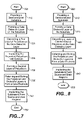
- FIG. 7 Another implementation of the present invention is illustrated in FIG. 7 .
- a semiconductor substrate is provided in a step 710 , and a gate dielectric layer is formed in a step 715 .
- a first thin layer of polysilicon (e.g., about 100–200 ⁇ thick for a 0.1 micron device size regime) is deposited over the substrate in step 720 .
- This layer of polysilicon may contain boron upon application or may be doped with boron after application.
- a lower-energy and lower dose calcium implantation than that described in connection with FIG. 6 is performed—for example, implantation energy in the range of 1–5 keV at a dose of 0.2e15/cm 2 to 1e15/cm 2 .
- a second layer of polysilicon (e.g., about 800–1400 ⁇ thick) is applied. As in step 720 , this layer may or may not contain boron, and the boron may be added after application of the layer.
- FIG. 7 ends with steps 735 and 740 , which are identical to steps 635 and 640 as described with respect to FIG. 6 .
- FIG. 8 A further alternative implementation of the present invention is illustrated in FIG. 8 .
- this variation begins with providing a semiconductor substrate in a step 810 and the application of a gate dielectric layer in a step 815 .
- a layer of calcium-doped polysilicon is applied, generally by deposition, for example, by chemical vapor deposition (CVD) over the gate dielectric layer.
- CVD chemical vapor deposition
- the polysilicon layer may also contain boron, either by deposition or by subsequent implantation doping.
- FIG. 8 ends with steps 835 and 840 , which are identical to steps 635 and 640 as described with respect to FIG. 6 .
- a separate layer of calcium may be applied in a thin atomic layer (e.g., from about 1 to 3 atoms thick) between the layer of polysilicon and the gate electrode by atomic layer deposition (ALD) or some other method.
- ALD atomic layer deposition
Landscapes
- Insulated Gate Type Field-Effect Transistor (AREA)
- Electrodes Of Semiconductors (AREA)
Abstract
Description
Claims (25)
Priority Applications (1)
| Application Number | Priority Date | Filing Date | Title |
|---|---|---|---|
| US10/698,167 US6930362B1 (en) | 2003-10-30 | 2003-10-30 | Calcium doped polysilicon gate electrodes |
Applications Claiming Priority (1)
| Application Number | Priority Date | Filing Date | Title |
|---|---|---|---|
| US10/698,167 US6930362B1 (en) | 2003-10-30 | 2003-10-30 | Calcium doped polysilicon gate electrodes |
Publications (1)
| Publication Number | Publication Date |
|---|---|
| US6930362B1 true US6930362B1 (en) | 2005-08-16 |
Family
ID=34826332
Family Applications (1)
| Application Number | Title | Priority Date | Filing Date |
|---|---|---|---|
| US10/698,167 Expired - Fee Related US6930362B1 (en) | 2003-10-30 | 2003-10-30 | Calcium doped polysilicon gate electrodes |
Country Status (1)
| Country | Link |
|---|---|
| US (1) | US6930362B1 (en) |
Cited By (3)
| Publication number | Priority date | Publication date | Assignee | Title |
|---|---|---|---|---|
| US20070194385A1 (en) * | 2004-10-01 | 2007-08-23 | Martin Dale W | Gate stacks |
| US20080173958A1 (en) * | 2007-01-22 | 2008-07-24 | Infineon Technologies North America Corp. | Semiconductor Device with Pre-Anneal Sandwich Gate Structure, and Method of Manufacturing |
| US9947767B1 (en) | 2017-01-26 | 2018-04-17 | International Business Machines Corporation | Self-limited inner spacer formation for gate-all-around field effect transistors |
Citations (7)
| Publication number | Priority date | Publication date | Assignee | Title |
|---|---|---|---|---|
| US4755865A (en) * | 1986-01-21 | 1988-07-05 | Motorola Inc. | Means for stabilizing polycrystalline semiconductor layers |
| US5937303A (en) * | 1997-10-29 | 1999-08-10 | Advanced Micro Devices | High dielectric constant gate dielectric integrated with nitrogenated gate electrode |
| US6373113B1 (en) * | 1996-12-10 | 2002-04-16 | Advanced Micro Devices, Inc. | Nitrogenated gate structure for improved transistor performance and method for making same |
| US20030168705A1 (en) * | 2002-03-07 | 2003-09-11 | Fujitsu Limited | Semiconductor device and method for fabricating the same |
| US20040089887A1 (en) * | 2002-11-08 | 2004-05-13 | Lsi Logic Corporation | High-K dielectric gate material uniquely formed |
| US20040110328A1 (en) * | 2002-12-06 | 2004-06-10 | Sheldon Aronowitz | Process to minimize polysilicon gate depletion and dopant penetration and to increase conductivity |
| US20040121550A1 (en) * | 2002-12-19 | 2004-06-24 | Vladimir Zubkov | Method for creating barriers to metal contamination in silicon oxides |
-
2003
- 2003-10-30 US US10/698,167 patent/US6930362B1/en not_active Expired - Fee Related
Patent Citations (7)
| Publication number | Priority date | Publication date | Assignee | Title |
|---|---|---|---|---|
| US4755865A (en) * | 1986-01-21 | 1988-07-05 | Motorola Inc. | Means for stabilizing polycrystalline semiconductor layers |
| US6373113B1 (en) * | 1996-12-10 | 2002-04-16 | Advanced Micro Devices, Inc. | Nitrogenated gate structure for improved transistor performance and method for making same |
| US5937303A (en) * | 1997-10-29 | 1999-08-10 | Advanced Micro Devices | High dielectric constant gate dielectric integrated with nitrogenated gate electrode |
| US20030168705A1 (en) * | 2002-03-07 | 2003-09-11 | Fujitsu Limited | Semiconductor device and method for fabricating the same |
| US20040089887A1 (en) * | 2002-11-08 | 2004-05-13 | Lsi Logic Corporation | High-K dielectric gate material uniquely formed |
| US20040110328A1 (en) * | 2002-12-06 | 2004-06-10 | Sheldon Aronowitz | Process to minimize polysilicon gate depletion and dopant penetration and to increase conductivity |
| US20040121550A1 (en) * | 2002-12-19 | 2004-06-24 | Vladimir Zubkov | Method for creating barriers to metal contamination in silicon oxides |
Cited By (9)
| Publication number | Priority date | Publication date | Assignee | Title |
|---|---|---|---|---|
| US20070194385A1 (en) * | 2004-10-01 | 2007-08-23 | Martin Dale W | Gate stacks |
| US7378712B2 (en) * | 2004-10-01 | 2008-05-27 | International Business Machines Corporation | Gate stacks |
| US20080173958A1 (en) * | 2007-01-22 | 2008-07-24 | Infineon Technologies North America Corp. | Semiconductor Device with Pre-Anneal Sandwich Gate Structure, and Method of Manufacturing |
| US7842579B2 (en) | 2007-01-22 | 2010-11-30 | Infineon Technologies Ag | Method for manufacturing a semiconductor device having doped and undoped polysilicon layers |
| US20110031563A1 (en) * | 2007-01-22 | 2011-02-10 | Infineon Technologies North America Corp. | Method for Manufacturing a Semiconductor Device Having Doped and Undoped Polysilicon Layers |
| US8063406B2 (en) | 2007-01-22 | 2011-11-22 | Infineon Technologies Ag | Semiconductor device having a polysilicon layer with a non-constant doping profile |
| US9947767B1 (en) | 2017-01-26 | 2018-04-17 | International Business Machines Corporation | Self-limited inner spacer formation for gate-all-around field effect transistors |
| US10326001B2 (en) * | 2017-01-26 | 2019-06-18 | International Business Machines Corporation | Self-limited inner spacer formation for gate-all-around field effect transistors |
| US10453937B2 (en) | 2017-01-26 | 2019-10-22 | International Business Machines Corporation | Self-limited inner spacer formation for gate-all-around field effect transistors |
Similar Documents
| Publication | Publication Date | Title |
|---|---|---|
| US9024384B2 (en) | Indium, carbon and halogen doping for PMOS transistors | |
| KR100618815B1 (en) | Semiconductor device having heterogeneous gate insulating film and manufacturing method thereof | |
| US7754570B2 (en) | Semiconductor device | |
| US6589827B2 (en) | Semiconductor device and method for fabricating the same | |
| US8853042B2 (en) | Carbon and nitrogen doping for selected PMOS transistors on an integrated circuit | |
| US6287897B1 (en) | Gate dielectric with self forming diffusion barrier | |
| US20040087124A1 (en) | Method for fabricating semiconductor device | |
| US20030082863A1 (en) | CMOS of semiconductor device and method for manufacturing the same | |
| US8232605B2 (en) | Method for gate leakage reduction and Vt shift control and complementary metal-oxide-semiconductor device | |
| CN1885560A (en) | Method to control flatband/threshold voltage in high-k metal gated stacks and structures thereof | |
| KR100687153B1 (en) | Semiconductor device and manufacturing method thereof | |
| CN1996617A (en) | Semiconductor device and method of manufacturing the same | |
| US20080142910A1 (en) | Semiconductor device | |
| CN1841772A (en) | Semiconductor device and method for fabricating the same | |
| US7947547B2 (en) | Method for manufacturing a semiconductor device | |
| US6617214B2 (en) | Integrated circuit structure and method therefore | |
| US6930362B1 (en) | Calcium doped polysilicon gate electrodes | |
| US8716812B2 (en) | Interfacial layer regrowth control in high-K gate structure for field effect transistor | |
| KR101858524B1 (en) | Manufacturing method for semiconductor device | |
| US20100123200A1 (en) | Semiconductor device and method of manufacturing the same | |
| US6878583B2 (en) | Integration method to enhance p+ gate activation | |
| CN1716618A (en) | Full lack of SOI multi-threshold voltage applications | |
| KR100336572B1 (en) | Method for forming semiconductor device with gate electrode using poly silicon-germanium | |
| US6864141B1 (en) | Method of incorporating nitrogen into metal silicate based dielectrics by energized nitrogen ion beams | |
| JPH1065152A (en) | Manufacturing method for semiconductor device |
Legal Events
| Date | Code | Title | Description |
|---|---|---|---|
| AS | Assignment |
Owner name: LSI LOGIC CORPORATION, CALIFORNIA Free format text: ASSIGNMENT OF ASSIGNORS INTEREST;ASSIGNORS:MIRABEDINI, MOHAMMAD R.;SUN, GRACE S.;REEL/FRAME:014657/0849;SIGNING DATES FROM 20030417 TO 20030515 |
|
| FEPP | Fee payment procedure |
Free format text: PAYOR NUMBER ASSIGNED (ORIGINAL EVENT CODE: ASPN); ENTITY STATUS OF PATENT OWNER: LARGE ENTITY |
|
| FPAY | Fee payment |
Year of fee payment: 4 |
|
| FPAY | Fee payment |
Year of fee payment: 8 |
|
| AS | Assignment |
Owner name: DEUTSCHE BANK AG NEW YORK BRANCH, AS COLLATERAL AGENT, NEW YORK Free format text: PATENT SECURITY AGREEMENT;ASSIGNORS:LSI CORPORATION;AGERE SYSTEMS LLC;REEL/FRAME:032856/0031 Effective date: 20140506 Owner name: DEUTSCHE BANK AG NEW YORK BRANCH, AS COLLATERAL AG Free format text: PATENT SECURITY AGREEMENT;ASSIGNORS:LSI CORPORATION;AGERE SYSTEMS LLC;REEL/FRAME:032856/0031 Effective date: 20140506 |
|
| AS | Assignment |
Owner name: LSI CORPORATION, CALIFORNIA Free format text: CHANGE OF NAME;ASSIGNOR:LSI LOGIC CORPORATION;REEL/FRAME:033102/0270 Effective date: 20070406 |
|
| AS | Assignment |
Owner name: AVAGO TECHNOLOGIES GENERAL IP (SINGAPORE) PTE. LTD Free format text: ASSIGNMENT OF ASSIGNORS INTEREST;ASSIGNOR:LSI CORPORATION;REEL/FRAME:035390/0388 Effective date: 20140814 |
|
| AS | Assignment |
Owner name: LSI CORPORATION, CALIFORNIA Free format text: TERMINATION AND RELEASE OF SECURITY INTEREST IN PATENT RIGHTS (RELEASES RF 032856-0031);ASSIGNOR:DEUTSCHE BANK AG NEW YORK BRANCH, AS COLLATERAL AGENT;REEL/FRAME:037684/0039 Effective date: 20160201 Owner name: AGERE SYSTEMS LLC, PENNSYLVANIA Free format text: TERMINATION AND RELEASE OF SECURITY INTEREST IN PATENT RIGHTS (RELEASES RF 032856-0031);ASSIGNOR:DEUTSCHE BANK AG NEW YORK BRANCH, AS COLLATERAL AGENT;REEL/FRAME:037684/0039 Effective date: 20160201 |
|
| AS | Assignment |
Owner name: BANK OF AMERICA, N.A., AS COLLATERAL AGENT, NORTH CAROLINA Free format text: PATENT SECURITY AGREEMENT;ASSIGNOR:AVAGO TECHNOLOGIES GENERAL IP (SINGAPORE) PTE. LTD.;REEL/FRAME:037808/0001 Effective date: 20160201 Owner name: BANK OF AMERICA, N.A., AS COLLATERAL AGENT, NORTH Free format text: PATENT SECURITY AGREEMENT;ASSIGNOR:AVAGO TECHNOLOGIES GENERAL IP (SINGAPORE) PTE. LTD.;REEL/FRAME:037808/0001 Effective date: 20160201 |
|
| AS | Assignment |
Owner name: AVAGO TECHNOLOGIES GENERAL IP (SINGAPORE) PTE. LTD., SINGAPORE Free format text: TERMINATION AND RELEASE OF SECURITY INTEREST IN PATENTS;ASSIGNOR:BANK OF AMERICA, N.A., AS COLLATERAL AGENT;REEL/FRAME:041710/0001 Effective date: 20170119 Owner name: AVAGO TECHNOLOGIES GENERAL IP (SINGAPORE) PTE. LTD Free format text: TERMINATION AND RELEASE OF SECURITY INTEREST IN PATENTS;ASSIGNOR:BANK OF AMERICA, N.A., AS COLLATERAL AGENT;REEL/FRAME:041710/0001 Effective date: 20170119 |
|
| REMI | Maintenance fee reminder mailed | ||
| LAPS | Lapse for failure to pay maintenance fees |
Free format text: PATENT EXPIRED FOR FAILURE TO PAY MAINTENANCE FEES (ORIGINAL EVENT CODE: EXP.) |
|
| STCH | Information on status: patent discontinuation |
Free format text: PATENT EXPIRED DUE TO NONPAYMENT OF MAINTENANCE FEES UNDER 37 CFR 1.362 |
|
| FP | Lapsed due to failure to pay maintenance fee |
Effective date: 20170816 |
|
| AS | Assignment |
Owner name: BELL SEMICONDUCTOR, LLC, ILLINOIS Free format text: ASSIGNMENT OF ASSIGNORS INTEREST;ASSIGNORS:AVAGO TECHNOLOGIES GENERAL IP (SINGAPORE) PTE. LTD.;BROADCOM CORPORATION;REEL/FRAME:044886/0001 Effective date: 20171208 |
|
| AS | Assignment |
Owner name: CORTLAND CAPITAL MARKET SERVICES LLC, AS COLLATERAL AGENT, ILLINOIS Free format text: SECURITY INTEREST;ASSIGNORS:HILCO PATENT ACQUISITION 56, LLC;BELL SEMICONDUCTOR, LLC;BELL NORTHERN RESEARCH, LLC;REEL/FRAME:045216/0020 Effective date: 20180124 Owner name: CORTLAND CAPITAL MARKET SERVICES LLC, AS COLLATERA Free format text: SECURITY INTEREST;ASSIGNORS:HILCO PATENT ACQUISITION 56, LLC;BELL SEMICONDUCTOR, LLC;BELL NORTHERN RESEARCH, LLC;REEL/FRAME:045216/0020 Effective date: 20180124 |
|
| AS | Assignment |
Owner name: BELL NORTHERN RESEARCH, LLC, ILLINOIS Free format text: SECURITY INTEREST;ASSIGNOR:CORTLAND CAPITAL MARKET SERVICES LLC;REEL/FRAME:060885/0001 Effective date: 20220401 Owner name: BELL SEMICONDUCTOR, LLC, ILLINOIS Free format text: SECURITY INTEREST;ASSIGNOR:CORTLAND CAPITAL MARKET SERVICES LLC;REEL/FRAME:060885/0001 Effective date: 20220401 Owner name: HILCO PATENT ACQUISITION 56, LLC, ILLINOIS Free format text: SECURITY INTEREST;ASSIGNOR:CORTLAND CAPITAL MARKET SERVICES LLC;REEL/FRAME:060885/0001 Effective date: 20220401 |