US6893543B1 - Information carrier and method for producing the same - Google Patents
Information carrier and method for producing the same Download PDFInfo
- Publication number
- US6893543B1 US6893543B1 US09/362,397 US36239799A US6893543B1 US 6893543 B1 US6893543 B1 US 6893543B1 US 36239799 A US36239799 A US 36239799A US 6893543 B1 US6893543 B1 US 6893543B1
- Authority
- US
- United States
- Prior art keywords
- layer
- solid material
- information
- intermediate layer
- radiation
- Prior art date
- Legal status (The legal status is an assumption and is not a legal conclusion. Google has not performed a legal analysis and makes no representation as to the accuracy of the status listed.)
- Expired - Fee Related, expires
Links
Images


Classifications
-
- G—PHYSICS
- G11—INFORMATION STORAGE
- G11B—INFORMATION STORAGE BASED ON RELATIVE MOVEMENT BETWEEN RECORD CARRIER AND TRANSDUCER
- G11B11/00—Recording on or reproducing from the same record carrier wherein for these two operations the methods are covered by different main groups of groups G11B3/00 - G11B7/00 or by different subgroups of group G11B9/00; Record carriers therefor
- G11B11/10—Recording on or reproducing from the same record carrier wherein for these two operations the methods are covered by different main groups of groups G11B3/00 - G11B7/00 or by different subgroups of group G11B9/00; Record carriers therefor using recording by magnetic means or other means for magnetisation or demagnetisation of a record carrier, e.g. light induced spin magnetisation; Demagnetisation by thermal or stress means in the presence or not of an orienting magnetic field
- G11B11/105—Recording on or reproducing from the same record carrier wherein for these two operations the methods are covered by different main groups of groups G11B3/00 - G11B7/00 or by different subgroups of group G11B9/00; Record carriers therefor using recording by magnetic means or other means for magnetisation or demagnetisation of a record carrier, e.g. light induced spin magnetisation; Demagnetisation by thermal or stress means in the presence or not of an orienting magnetic field using a beam of light or a magnetic field for recording by change of magnetisation and a beam of light for reproducing, i.e. magneto-optical, e.g. light-induced thermomagnetic recording, spin magnetisation recording, Kerr or Faraday effect reproducing
- G11B11/10582—Record carriers characterised by the selection of the material or by the structure or form
- G11B11/10586—Record carriers characterised by the selection of the material or by the structure or form characterised by the selection of the material
-
- C—CHEMISTRY; METALLURGY
- C23—COATING METALLIC MATERIAL; COATING MATERIAL WITH METALLIC MATERIAL; CHEMICAL SURFACE TREATMENT; DIFFUSION TREATMENT OF METALLIC MATERIAL; COATING BY VACUUM EVAPORATION, BY SPUTTERING, BY ION IMPLANTATION OR BY CHEMICAL VAPOUR DEPOSITION, IN GENERAL; INHIBITING CORROSION OF METALLIC MATERIAL OR INCRUSTATION IN GENERAL
- C23C—COATING METALLIC MATERIAL; COATING MATERIAL WITH METALLIC MATERIAL; SURFACE TREATMENT OF METALLIC MATERIAL BY DIFFUSION INTO THE SURFACE, BY CHEMICAL CONVERSION OR SUBSTITUTION; COATING BY VACUUM EVAPORATION, BY SPUTTERING, BY ION IMPLANTATION OR BY CHEMICAL VAPOUR DEPOSITION, IN GENERAL
- C23C14/00—Coating by vacuum evaporation, by sputtering or by ion implantation of the coating forming material
- C23C14/0021—Reactive sputtering or evaporation
-
- C—CHEMISTRY; METALLURGY
- C23—COATING METALLIC MATERIAL; COATING MATERIAL WITH METALLIC MATERIAL; CHEMICAL SURFACE TREATMENT; DIFFUSION TREATMENT OF METALLIC MATERIAL; COATING BY VACUUM EVAPORATION, BY SPUTTERING, BY ION IMPLANTATION OR BY CHEMICAL VAPOUR DEPOSITION, IN GENERAL; INHIBITING CORROSION OF METALLIC MATERIAL OR INCRUSTATION IN GENERAL
- C23C—COATING METALLIC MATERIAL; COATING MATERIAL WITH METALLIC MATERIAL; SURFACE TREATMENT OF METALLIC MATERIAL BY DIFFUSION INTO THE SURFACE, BY CHEMICAL CONVERSION OR SUBSTITUTION; COATING BY VACUUM EVAPORATION, BY SPUTTERING, BY ION IMPLANTATION OR BY CHEMICAL VAPOUR DEPOSITION, IN GENERAL
- C23C14/00—Coating by vacuum evaporation, by sputtering or by ion implantation of the coating forming material
- C23C14/06—Coating by vacuum evaporation, by sputtering or by ion implantation of the coating forming material characterised by the coating material
- C23C14/0635—Carbides
-
- C—CHEMISTRY; METALLURGY
- C23—COATING METALLIC MATERIAL; COATING MATERIAL WITH METALLIC MATERIAL; CHEMICAL SURFACE TREATMENT; DIFFUSION TREATMENT OF METALLIC MATERIAL; COATING BY VACUUM EVAPORATION, BY SPUTTERING, BY ION IMPLANTATION OR BY CHEMICAL VAPOUR DEPOSITION, IN GENERAL; INHIBITING CORROSION OF METALLIC MATERIAL OR INCRUSTATION IN GENERAL
- C23C—COATING METALLIC MATERIAL; COATING MATERIAL WITH METALLIC MATERIAL; SURFACE TREATMENT OF METALLIC MATERIAL BY DIFFUSION INTO THE SURFACE, BY CHEMICAL CONVERSION OR SUBSTITUTION; COATING BY VACUUM EVAPORATION, BY SPUTTERING, BY ION IMPLANTATION OR BY CHEMICAL VAPOUR DEPOSITION, IN GENERAL
- C23C14/00—Coating by vacuum evaporation, by sputtering or by ion implantation of the coating forming material
- C23C14/06—Coating by vacuum evaporation, by sputtering or by ion implantation of the coating forming material characterised by the coating material
- C23C14/0641—Nitrides
- C23C14/0647—Boron nitride
-
- G—PHYSICS
- G11—INFORMATION STORAGE
- G11B—INFORMATION STORAGE BASED ON RELATIVE MOVEMENT BETWEEN RECORD CARRIER AND TRANSDUCER
- G11B7/00—Recording or reproducing by optical means, e.g. recording using a thermal beam of optical radiation by modifying optical properties or the physical structure, reproducing using an optical beam at lower power by sensing optical properties; Record carriers therefor
- G11B7/24—Record carriers characterised by shape, structure or physical properties, or by the selection of the material
- G11B7/241—Record carriers characterised by shape, structure or physical properties, or by the selection of the material characterised by the selection of the material
- G11B7/252—Record carriers characterised by shape, structure or physical properties, or by the selection of the material characterised by the selection of the material of layers other than recording layers
- G11B7/254—Record carriers characterised by shape, structure or physical properties, or by the selection of the material characterised by the selection of the material of layers other than recording layers of protective topcoat layers
-
- G—PHYSICS
- G11—INFORMATION STORAGE
- G11B—INFORMATION STORAGE BASED ON RELATIVE MOVEMENT BETWEEN RECORD CARRIER AND TRANSDUCER
- G11B7/00—Recording or reproducing by optical means, e.g. recording using a thermal beam of optical radiation by modifying optical properties or the physical structure, reproducing using an optical beam at lower power by sensing optical properties; Record carriers therefor
- G11B7/24—Record carriers characterised by shape, structure or physical properties, or by the selection of the material
- G11B7/241—Record carriers characterised by shape, structure or physical properties, or by the selection of the material characterised by the selection of the material
- G11B7/252—Record carriers characterised by shape, structure or physical properties, or by the selection of the material characterised by the selection of the material of layers other than recording layers
- G11B7/257—Record carriers characterised by shape, structure or physical properties, or by the selection of the material characterised by the selection of the material of layers other than recording layers of layers having properties involved in recording or reproduction, e.g. optical interference layers or sensitising layers or dielectric layers, which are protecting the recording layers
- G11B7/2578—Record carriers characterised by shape, structure or physical properties, or by the selection of the material characterised by the selection of the material of layers other than recording layers of layers having properties involved in recording or reproduction, e.g. optical interference layers or sensitising layers or dielectric layers, which are protecting the recording layers consisting essentially of inorganic materials
-
- G—PHYSICS
- G11—INFORMATION STORAGE
- G11B—INFORMATION STORAGE BASED ON RELATIVE MOVEMENT BETWEEN RECORD CARRIER AND TRANSDUCER
- G11B7/00—Recording or reproducing by optical means, e.g. recording using a thermal beam of optical radiation by modifying optical properties or the physical structure, reproducing using an optical beam at lower power by sensing optical properties; Record carriers therefor
- G11B7/24—Record carriers characterised by shape, structure or physical properties, or by the selection of the material
- G11B7/26—Apparatus or processes specially adapted for the manufacture of record carriers
-
- G—PHYSICS
- G11—INFORMATION STORAGE
- G11B—INFORMATION STORAGE BASED ON RELATIVE MOVEMENT BETWEEN RECORD CARRIER AND TRANSDUCER
- G11B7/00—Recording or reproducing by optical means, e.g. recording using a thermal beam of optical radiation by modifying optical properties or the physical structure, reproducing using an optical beam at lower power by sensing optical properties; Record carriers therefor
- G11B7/24—Record carriers characterised by shape, structure or physical properties, or by the selection of the material
- G11B7/241—Record carriers characterised by shape, structure or physical properties, or by the selection of the material characterised by the selection of the material
- G11B7/252—Record carriers characterised by shape, structure or physical properties, or by the selection of the material characterised by the selection of the material of layers other than recording layers
- G11B7/257—Record carriers characterised by shape, structure or physical properties, or by the selection of the material characterised by the selection of the material of layers other than recording layers of layers having properties involved in recording or reproduction, e.g. optical interference layers or sensitising layers or dielectric layers, which are protecting the recording layers
- G11B2007/25705—Record carriers characterised by shape, structure or physical properties, or by the selection of the material characterised by the selection of the material of layers other than recording layers of layers having properties involved in recording or reproduction, e.g. optical interference layers or sensitising layers or dielectric layers, which are protecting the recording layers consisting essentially of inorganic materials
- G11B2007/25706—Record carriers characterised by shape, structure or physical properties, or by the selection of the material characterised by the selection of the material of layers other than recording layers of layers having properties involved in recording or reproduction, e.g. optical interference layers or sensitising layers or dielectric layers, which are protecting the recording layers consisting essentially of inorganic materials containing transition metal elements (Zn, Fe, Co, Ni, Pt)
-
- G—PHYSICS
- G11—INFORMATION STORAGE
- G11B—INFORMATION STORAGE BASED ON RELATIVE MOVEMENT BETWEEN RECORD CARRIER AND TRANSDUCER
- G11B7/00—Recording or reproducing by optical means, e.g. recording using a thermal beam of optical radiation by modifying optical properties or the physical structure, reproducing using an optical beam at lower power by sensing optical properties; Record carriers therefor
- G11B7/24—Record carriers characterised by shape, structure or physical properties, or by the selection of the material
- G11B7/241—Record carriers characterised by shape, structure or physical properties, or by the selection of the material characterised by the selection of the material
- G11B7/252—Record carriers characterised by shape, structure or physical properties, or by the selection of the material characterised by the selection of the material of layers other than recording layers
- G11B7/257—Record carriers characterised by shape, structure or physical properties, or by the selection of the material characterised by the selection of the material of layers other than recording layers of layers having properties involved in recording or reproduction, e.g. optical interference layers or sensitising layers or dielectric layers, which are protecting the recording layers
- G11B2007/25705—Record carriers characterised by shape, structure or physical properties, or by the selection of the material characterised by the selection of the material of layers other than recording layers of layers having properties involved in recording or reproduction, e.g. optical interference layers or sensitising layers or dielectric layers, which are protecting the recording layers consisting essentially of inorganic materials
- G11B2007/2571—Record carriers characterised by shape, structure or physical properties, or by the selection of the material characterised by the selection of the material of layers other than recording layers of layers having properties involved in recording or reproduction, e.g. optical interference layers or sensitising layers or dielectric layers, which are protecting the recording layers consisting essentially of inorganic materials containing group 14 elements except carbon (Si, Ge, Sn, Pb)
-
- G—PHYSICS
- G11—INFORMATION STORAGE
- G11B—INFORMATION STORAGE BASED ON RELATIVE MOVEMENT BETWEEN RECORD CARRIER AND TRANSDUCER
- G11B7/00—Recording or reproducing by optical means, e.g. recording using a thermal beam of optical radiation by modifying optical properties or the physical structure, reproducing using an optical beam at lower power by sensing optical properties; Record carriers therefor
- G11B7/24—Record carriers characterised by shape, structure or physical properties, or by the selection of the material
- G11B7/241—Record carriers characterised by shape, structure or physical properties, or by the selection of the material characterised by the selection of the material
- G11B7/252—Record carriers characterised by shape, structure or physical properties, or by the selection of the material characterised by the selection of the material of layers other than recording layers
- G11B7/257—Record carriers characterised by shape, structure or physical properties, or by the selection of the material characterised by the selection of the material of layers other than recording layers of layers having properties involved in recording or reproduction, e.g. optical interference layers or sensitising layers or dielectric layers, which are protecting the recording layers
- G11B2007/25705—Record carriers characterised by shape, structure or physical properties, or by the selection of the material characterised by the selection of the material of layers other than recording layers of layers having properties involved in recording or reproduction, e.g. optical interference layers or sensitising layers or dielectric layers, which are protecting the recording layers consisting essentially of inorganic materials
- G11B2007/25711—Record carriers characterised by shape, structure or physical properties, or by the selection of the material characterised by the selection of the material of layers other than recording layers of layers having properties involved in recording or reproduction, e.g. optical interference layers or sensitising layers or dielectric layers, which are protecting the recording layers consisting essentially of inorganic materials containing carbon
-
- G—PHYSICS
- G11—INFORMATION STORAGE
- G11B—INFORMATION STORAGE BASED ON RELATIVE MOVEMENT BETWEEN RECORD CARRIER AND TRANSDUCER
- G11B7/00—Recording or reproducing by optical means, e.g. recording using a thermal beam of optical radiation by modifying optical properties or the physical structure, reproducing using an optical beam at lower power by sensing optical properties; Record carriers therefor
- G11B7/24—Record carriers characterised by shape, structure or physical properties, or by the selection of the material
- G11B7/241—Record carriers characterised by shape, structure or physical properties, or by the selection of the material characterised by the selection of the material
- G11B7/252—Record carriers characterised by shape, structure or physical properties, or by the selection of the material characterised by the selection of the material of layers other than recording layers
- G11B7/257—Record carriers characterised by shape, structure or physical properties, or by the selection of the material characterised by the selection of the material of layers other than recording layers of layers having properties involved in recording or reproduction, e.g. optical interference layers or sensitising layers or dielectric layers, which are protecting the recording layers
- G11B2007/25705—Record carriers characterised by shape, structure or physical properties, or by the selection of the material characterised by the selection of the material of layers other than recording layers of layers having properties involved in recording or reproduction, e.g. optical interference layers or sensitising layers or dielectric layers, which are protecting the recording layers consisting essentially of inorganic materials
- G11B2007/25713—Record carriers characterised by shape, structure or physical properties, or by the selection of the material characterised by the selection of the material of layers other than recording layers of layers having properties involved in recording or reproduction, e.g. optical interference layers or sensitising layers or dielectric layers, which are protecting the recording layers consisting essentially of inorganic materials containing nitrogen
-
- G—PHYSICS
- G11—INFORMATION STORAGE
- G11B—INFORMATION STORAGE BASED ON RELATIVE MOVEMENT BETWEEN RECORD CARRIER AND TRANSDUCER
- G11B7/00—Recording or reproducing by optical means, e.g. recording using a thermal beam of optical radiation by modifying optical properties or the physical structure, reproducing using an optical beam at lower power by sensing optical properties; Record carriers therefor
- G11B7/24—Record carriers characterised by shape, structure or physical properties, or by the selection of the material
- G11B7/241—Record carriers characterised by shape, structure or physical properties, or by the selection of the material characterised by the selection of the material
- G11B7/252—Record carriers characterised by shape, structure or physical properties, or by the selection of the material characterised by the selection of the material of layers other than recording layers
- G11B7/253—Record carriers characterised by shape, structure or physical properties, or by the selection of the material characterised by the selection of the material of layers other than recording layers of substrates
- G11B7/2533—Record carriers characterised by shape, structure or physical properties, or by the selection of the material characterised by the selection of the material of layers other than recording layers of substrates comprising resins
- G11B7/2534—Record carriers characterised by shape, structure or physical properties, or by the selection of the material characterised by the selection of the material of layers other than recording layers of substrates comprising resins polycarbonates [PC]
-
- G—PHYSICS
- G11—INFORMATION STORAGE
- G11B—INFORMATION STORAGE BASED ON RELATIVE MOVEMENT BETWEEN RECORD CARRIER AND TRANSDUCER
- G11B7/00—Recording or reproducing by optical means, e.g. recording using a thermal beam of optical radiation by modifying optical properties or the physical structure, reproducing using an optical beam at lower power by sensing optical properties; Record carriers therefor
- G11B7/24—Record carriers characterised by shape, structure or physical properties, or by the selection of the material
- G11B7/241—Record carriers characterised by shape, structure or physical properties, or by the selection of the material characterised by the selection of the material
- G11B7/252—Record carriers characterised by shape, structure or physical properties, or by the selection of the material characterised by the selection of the material of layers other than recording layers
- G11B7/258—Record carriers characterised by shape, structure or physical properties, or by the selection of the material characterised by the selection of the material of layers other than recording layers of reflective layers
- G11B7/2585—Record carriers characterised by shape, structure or physical properties, or by the selection of the material characterised by the selection of the material of layers other than recording layers of reflective layers based on aluminium
Definitions
- the present invention is generally directed to an information carrier, comprising at least two-solid material interfaces, at which information is applied or may be applied by local modulation of at least one solid material characteristic, from which reflection of electromagnetic radiation depends on at said interfaces, and which further comprises at least one intermediate layer between the two solid material interfaces, which layer transmits the said radiation at least to a considerable amount.
- the present invention is further generally directed to a method for producing a layer, which at least predominantly consists of Si x C y or of Si x C y H z or of Si v N w or of Si v N w H u by means of a reactive vacuum coating process, and further is directed to a vacuum coating apparatus which is specifically suited for performing the said method of producing the said layer.
- the method for producing the said layer is particularly suited for producing at least one layer at the said intermediate layer of the information carrier.
- MMCD or “single sided dual layer high-density CD” or “hdCD” are known-as optical information carrier in the shape of CDs, at which the information density is considerably improved.
- This is achieved by providing two solid material interfaces, whereat information is stored on a carrier substrate.
- the solid material interfaces are separated by means of an intermediate layer.
- the information at the solid material interfaces is applied by local modulation of a surface pattern of intrusions at one of the material surfaces forming the interface.
- Reading information is realized by means of a beam of electromagnetic radiation in the form of laser light of 635 nm or 650 nm wavelength or especially of 450 nm.
- the intermediate layer between the information carrying solid material interfaces is practically transmittant to 100% at those wavelengths, so that a part of the impinging beam energy is reflected at the one information carrying solid material interface and a second part at the second.
- hybrid MMCD whereat the information provided at respective ones of two information carrying solid material interfaces is selectively read by means of radiation at different wavelengths, namely, on the one hand, by means of a laser beam with a wavelength of light of 635 nm and, on the other hand, with a laser beam with a wavelength of light at 786 nm.
- the present invention is most generically dealing with such information carriers, method for producing same and apparatus therefor, whereby it must be pointed out that, under this generic aspect, information at the said solid material interfaces may be applied by local modulation of surface structure, as at the well-known optical storage carriers, or may be provided or applied-at in the sense of magneto-optical storage as is known from the U.S. Pat. No. 5,158,834.
- the present invention under its most generic aspect, is not limited to information carriers which are already provided with stored information, as e.g. stored by mechanical forming process from a master as known from optical storage disks, but the present invention is also directed to information carriers which are yet empty of information and onto which the information is to be loaded or written.
- the intermediate layer comprises at least two layers, one of which being optically effective, especially contributing to reflection, the other of which primarily acting as a spacer.
- an information carrier which comprises at least two solid material interfaces, at which information is or may be applied and whereat the information is stored by local modulation of at least one solid material characteristic, from which characteristic reflection of electromagnetic radiation depends at said interfaces and which further comprises at least one intermediate layer between the two solid material interfaces, which intermediate layer transmits the radiation and which intermediate layer further comprises a layer which is at least predominantly of Si x C y or of Si v N w .
- an information carrier which comprises at least two solid material interfaces, at which information is or may be applied and whereat the information is stored by local modulation of at least one solid material characteristic, from which characteristic reflection of electromagnetic radiation depends at said interfaces, and which further comprises at least-one intermediate layer between the two solid material interfaces, which layer transmits the radiation, and wherein further the information which is readable from at least one of the solid material interfaces is readable by means of radiation of predetermined wavelength, whereby the intermediate layer comprises a dielectric layer system with at least one layer, wherein the dielectric layer system has an optical thickness D which, at least in a first approximation, is m ⁇ o /4, wherein m is integer and at least unity and is odd and wherein ⁇ o designates the wavelength of the radiation which is transmitted through-the at least one dielectric layer of the dielectric layer system.
- m may be selected smaller up to 0.6 to its integer value or up to 0.2 larger.
- a dielectric layer system of significantly reduced thickness may be used, thus significantly improving economic production.
- preferred dielectric layer materials are Si x C y , Si x C y H z , Si v N w or Si v N w H u , but also ZrN or even HfN and TiN may be applicable.
- x/y and respectively v/w should be larger than unity, that preferably x/y ⁇ 1.2 and respectively v/w ⁇ 1.2 and, even better, x/y ⁇ 2, respectively v/w ⁇ 1.6.
- the intermediate layer at the inventive information carrier allows, due to the reflection controlling characteristics of its material, namely due to refractive index n and to its transmission characteristics (low absorption), to provide even more than two, i.e. three or more information carrying solid material interfaces and to read information therefrom from one side and preferably with one radiation wavelength.
- the inventive methods shall fulfil at least one of the following objects:
- At least one of the objects mentioned above is realized by a method for producing a layer which at least-predominantly consists of at least one, preferably just one of Si x C y and of Si v N w H u by means of a reactive vacuum coating process, which method comprises the step of freeing silicon from a solid body into the process atmosphere and reacting the freed silicon in the process atmosphere with a reactive gas which contains at least one, preferably just one of C and N.
- At least one of the objects mentioned above is further resolved by a method for producing a layer, which at least predominantly consists of at least one, preferably just one of Si x C y H z and of Si v N w H u by means of a reactive vacuum coating process, wherein an optimum of transmission of the layer and of refractive index of the material of the layer is achieved by means of adjusting the concentration of a gas in the process atmosphere, which gas contains at least two of C, N and H, preferably just C and H or N and H.
- FIG. 1 schematically, an inventive intermediate layer at an inventive information carrier under its generic aspect
- FIG. 2 schematically, a section of an inventive optical information carrier with two information-carrying solid material interfaces
- FIG. 3 in a representation according to FIG. 2 , a section of an inventive information carrier with three information-carrying, solid material interfaces;
- FIG. 4 schematically, a first inventive apparatus for producing layers and for realizing the inventive methods for producing such layers
- FIG. 5 schematically, a second and preferred embodiment of an inventive apparatus for realizing either of the inventive methods and with an inventive target.
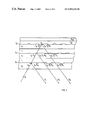
- FIG. 1 there is shown, principally, a section of a one-sided, bi- or multiple-reflecting information carrier according to the invention.
- An intermediate layer 3 is embedded between adjacent materials 2 o and 2 u .
- the intermediate layer comprises a dielectric layer 1 and a spacer layer 5 .
- the latter consists preferably of a lacquer, especially of an ultra-violet hardenable lacquer as e.g. of a 2P-lacquer of the firm Philips.
- the dielectric layer 1 far preferably consists of at least one of Si x C y H z and Si v N w H u , thereby preferably of one of these materials, at least to a predominant amount, but can also at least predominantly consist of Si x C y and/or Si v N w . It could be that even materials such as ZrN or HfN or TiN, and thereby preferably ZrN, may be used as material for the dielectric layer 1 .
- the material 2 u and layer 1 form a solid material interface 3 u .
- the material 2 o and the spacer layer 5 form a second solid material interface 3 o .
- an informative structure is applied or may be applied by local modulation of surface characteristics, as e.g. for optical information carriers, of the geometric structure and, for magneto-optical carriers, of the magnetic characteristics.
- the informative structure is shown in FIG. 1 principally by means of areas 7 .
- the modulated solid body characteristics i.e. for instance the said geometrical surface structure or magnetic surface structure, modulate impinging electromagnetic radiation 9 , as such radiation is shifted along the solid material interfaces 3 o and 3 u , as is perfectly known to the man skilled in this art.
- the electromagnetic radiation 9 with an intensity I o is, on one hand, reflected at the first solid material interface 3 u , according to a reflected part I o ⁇ R 2 , wherein R 2 is the factor of reflectance.
- This part I o ⁇ T 2 transits practically without loss through layer 5 and is reflected according to factor R 1 to become I o ⁇ R 1 T 2 .
- the transmission T 2 enters as a quadratic term T 2 2 into the expression for I 1 .
- the energy partitions are approximations which do not take account of the negligible influence of the optically inactive spacer layer 5 .
- the accurate distribution may be calculated with-the help of the program “Film*STAR”, Optical Thin Film Software, FTG Software Associates, P.O. Box 579, Princeton, N.J. 08542.
- the inventively applied layer 1 consists, at least predominantly, of Si x C y , Si x C y H z , Si v N w or Si v N w H u .
- the layer 1 thereby consists preferably of predominantly one of these materials; nevertheless, at least two of these four materials might be mixed.
- ⁇ o is the optical wavelength of the radiation 9 in the intermediate layer material, i.e. especially in the material of layer 1 .
- D G may be selected considerably smaller (thickness of layer!) than according to integer-valued m, whereby
- the reflection homogenity or distribution along solid material interface 3 o becomes significantly less dependent on thickness distribution or thickness variations of D G of the layer 1 on the material 2 u , which is with respect to the production method for depositing layer 1 a significant advantage.
- the spacer layer 5 is preferably formed by a lacquer which may be surface structured, as e.g. by a lacquer “2P” of the firm Philips, i.e. by a lacquer which may be hardened by ultra-violet radiation ( ⁇ s ⁇ 400 nm).
- a lacquer which may be surface structured, as e.g. by a lacquer “2P” of the firm Philips, i.e. by a lacquer which may be hardened by ultra-violet radiation ( ⁇ s ⁇ 400 nm).
- the inventive layer 1 has intrinsically a high transmission (low absorption) in the ultra-violet range, which may even be improved by the possibility mentioned above, namely to reduce the geometric thickness D G of layer 1 without significantly affecting reflection. Thereby, a transmission for ultra-violet range radiation is reached, which is at least 10%.
- the intermediate layer 3 especially at optical information carriers, is commonly deposited on a plastic material, as material 2 u , especially on surface structured polycarbonate or PMMA.
- a significant advantage of the inventive layer 1 may be seen in the fact that the preferred layer materials Si x C y and Si x C y H z as well as the said plastic substrate materials and the said lacquer contain carbon, so that rigid adherence of the layer material is achieved with respect to the said plastic material or lacquer.
- a very high index of refraction n 1 is required for the layer material, because the index of refraction of the substrate material is already high:
- the index of refraction of polycarbonate is e.g. 1.57. If, on the other hand, at the inventively applied material of layer 1 the index of refraction n 1 is increased, this will simultaneously lead to a decrease of transmission T 2 . i.e. to an increase of absorption in the material of layer 1 .
- the output signal from solid material interface 301 according to FIG. 1 is very critically dependent on a decrease of transmission T 2 (increase of absorption).
- Reflection R 1 is optimized by appropriate selection of the material 2 o according to FIG. 1 ; and was, e.g. using Al as material 2 o , 81% of the energy impinging on the second solid material interface.
- the inventive intermediate layer 3 with the inventive layer 1 may also be used for radiation within the blue spectral range, i.e. for light wavelength according to 400 nm ⁇ s ⁇ 500 nm.
- the inventive intermediate layer and layer may be used for applying radiation with selectively different wavelengths, as e.g. of 635 nm and 785 nm, for selectively reading information at one interface by light of one wavelength, and from the second interface by the light of the second wavelength.
- the optically effective layer 1 is tailored so that practically all 635 nm light is reflected at R 2 and practically all 785 nm light is transmitted onto solid material interface 30 and is reflected there. This is achieved by making the geometric thickness D G of layer 1 so as to accord with an odd number of quarter wavelengths with respect to the 635 nm light, and simultaneously to accord with an even number of quarter wavelengths for the 785 nm light.
- m is 0.4 ⁇ m ⁇ 1.2; (first order) 2.4 ⁇ m ⁇ 3.2; (third order) 4.4 ⁇ m ⁇ 5.5; (5th order)
- the inventive layer 1 fulfils, with respect to adherence, the adherence tape tests according to MIL-M-13508C and/or MIL-C-00675B, as defined in H. Pulker, “Coatings on Glass”, p. 358, Elsevier, 1984.
- FIG. 2 shows a preferred embodiment of an inventive optical information carrier, realized by an optical storage disk with two information carrying solid material interfaces 3 o ′, 3 u ′.
- a layer 1 is deposited according to the preferred specification under 1) to 3.8).
- a metallic reflection layer 2 o ′ made of A U or Ag, thereby preferably made of Al.
- the highly reflective layer 2 o ′ is covered with a covering layer 2 oD .
- each of the three solid material interfaces 3 u , 3 o1 ′, 3 o2 there is, preferably again at a laser light wavelength of 635 nm, reflected so much that each of the output beams S 1 to S 3 are of approximately 2% of the impinging energy I.
- inventive layer 1 is smaller than 2%, and the respective transmission T 2 is accordingly high.
- the embodiment according to FIG. 3 applied to the predescribed MMCD technique results in a storage capacity per one side of a 120 mm CD of approximately 11 GByte, whereas e.g. at a SD (super density disk) there results a storage capacity per side of approximately 13 GByte and for a double-sided SD of approximately 27 GByte.
- inventive reactive layer vacuum deposition apparatus which latter may not just exclusively be used for the above mentioned “semi-transparent” layers 1 at the inventive information carrier, but which are especially suited for that object.
- the “semi-transparent” layer 1 ( FIGS. 1 to 3 ) is deposited by means of ion plating, whereas in a preferred apparatus, according to FIG. 5 , and in a preferred manner, the inventive layer 1 is deposited by means of reactive sputter coating.
- the relation of transmission T 2 and index of refraction n 1 at the preferably deposited Si x C y H z and/or Si v N w H u layer is optimized by controlling the ratio of carbon to hydrogene.
- This is preferably realized by feeding at least two gases to the process atmosphere, which gases have different C/H or N/H content ratios each.
- the content of these two gases in the process atmosphere may be open-loop controlled or negative feedback controlled.
- a second alternative or additional aspect is that silicon atoms are freed into the process atmosphere from a highly pure silicon solid body and react in the process atmosphere with carbon-, preferably with carbon- and hydrogene-containing gas.
- the optical parameters are optimized.
- a noble gas as e.g. Ar, is used.
- carbon hydrogene gases as e.g. Butane C 4 H 10 , Methane CH 4 , Propane C 3 H 8 , Nitrogen N 2 or Nitrogen-hydrogen gases may be used, whereby, by open-loop or negative feedback loop controlling each gas flow to the process atmosphere, more or less carbon C or nitrogen-N is introduced per time unit compared with hydrogene fed to the process chamber per time unit.
- the silicon freed from the silicon solid body source, allows use of low price solid body sources compared, e.g., with the case where SiC is freed from well-known graphite-doped silicon sources.
- the overall layer deposition process becomes more controllable and, by varying process gas composition, adjustable.
- FIG. 4 which shows schematically an ion plating apparatus
- a plasma discharge PL in a vacuum chamber 51 between electrodes 53 and 54 , is maintained.
- silicon of a target 55 is evaporated or sputtered into the process atmosphere.
- a plasma discharge PL there may also be used, and as known to the skilled expert, thermic evaporation of silicon, as e.g. by means of electron beam.
- the plasma discharge PL may be operated either with Rf-voltage or with DC or with DC and superimposed Rf or with DC with superimposed medium frequency Mf-energy or with DC with superimposed low frequency Lf-signal, whereby, preferably, DC is used with superimposed Mf or Lf pulsating voltage.
- the plasma discharge PL is operated by means of a DC source 57 .
- Stability of the coating process is maintained in spite of the use of a low cost DC source 57 , by superimposing to the output signal of the DC source U m , an AC voltage with a frequency in the medium or low frequency range, which is preferably a pulsating voltage.
- this AC voltage is preferably intermittently superimposed at a superposition unit 58 to the output DC signal of source 57 .
- Such signal superposition is preferably realized by interconnecting the two discharge electrodes 53 and 54 intermittently by means of the chopper unit 59 , which intermittently interconnects these electrodes alternatively high ohmically and low ohmically.
- This preferred technique is shown in broken lines. Either a predetermined fixed chopper repetition rate and/or duty cycle is used or, and preferably, the occurrence of disturbance arcing is automatically monitored in the process recipient and controls via chopper unit 59 low ohmic connection of the two discharge electrodes 53 and 54 , thereby preventing arcing.
- a workpiece carrier electrode 60 which, e.g. with respect to electrode 54 , is fed with a negative DC electric potential by means of a DC source 62 .
- a superposition unit as was described, realized preferably by means of a chopper unit 64 , according to the predescribed chopper unit 59 , allows to maintain stability of the layer deposition process at the workpiece carrier electrode 60 .
- electric potential which is applied to the housing of the chamber, the electrodes 53 , 54 and 60 , the skilled expert knows different possibilities, also with respect to defining and applying reference, i.e. ground potential.
- a gas tank arrangement 66 is provided, from which a reactive gas G containing carbon C and/or nitrogen N 2 and preferably further hydrogene H is fed to the chamber 51 , i.e. into the process atmosphere.
- a reactive gas G containing carbon C and/or nitrogen N 2 and preferably further hydrogene H is fed to the chamber 51 , i.e. into the process atmosphere.
- a plasma discharge working gas which is normally selected to be Ar.
- the gas G results from controlled mixing of two gases G 1 and G 2 , as schematically shown, by means of controllable valves V 1 and V 2 . If the two gases, as e.g. Propane and Butane or Nitrogen and Ammonia, have different stochiometric ratios (e.g.
- Butane 2.5; Propane 2.7 the control of varying contents of the gases G 1 /G 2 in th process atmosphere controls the ratio of C/H or respectively of N/H in that atmosphere, and thus at the Si x C y H z or Si v N w H u layer which is growing.
- the transmission T 2 and the index of refraction n 1 at the growing Si x C y H z or Si v N w H u layer is controlled.
- FIG. 5 schematically shows, as an example, an apparatus for such magnetron sputtering.
- silicon is freed into the process atmosphere of the vacuum recipient 71 .
- the magnetron electrode 70 is connected to a workpiece carrier electrode 73 via a DC source 75 , as was described, whereby, again, a chopper arrangement 77 of the kind which was mentioned above is used (shown in dashed lines).
- This is a preferred realization of superimposing an AC voltage to the output DC voltage of the DC source 75 at the superposition unit 78 .
- the AC voltage is preferably selected as a medium frequency or low frequency signal, and is preferably pulsating.
- an inventive silicon target is preferably used, which is negatively or positively doped, preferably with Boron and/or Phosphor.
- the specific resistance of the target material made of doped silicon, ⁇ Si is: 0.01 ⁇ cm ⁇ Si ⁇ 6 ⁇ cm.
- the following is valid: 0.4 ⁇ cm ⁇ Si ⁇ 0.6 ⁇ cm.
- the per se low conductive silicon has an increased conductance ⁇ Si ⁇ 1 and may be even DC sputtered or, as was explained, preferably sputtered by means of a DC voltage with superimposed AC component.
- parallel chopper technique is preferably used.
- This mode of operation allows a most economic operation at a high deposition rate, whereby the silicon allows further to reach a high layer quality due to the fact that it is sputtered without arcing and without occurrence of droplet.
- the reactive gas G is applied as a single gas or as a gas mixture, as was explained with respect to FIG. 4 .
- the layers may be deposited with a magnetron source 70 , as known per se, so e.g. by placing the carrier substrates just in front of the target.
- the carrier substrate may also be moved along the target, so e.g. in linear in-line coaters, or may-be rotated passing the target, as e.g. in plants with rotating cylindrical workpiece carriers.
- An Si x C y H z layer was deposited on a polycarbonate substrate. Thereby, an apparatus was used as principally shown in FIG. 5 .
- the substrates were deposited on a cylindric carrier and were rotated passing a rectangular magnetron source. Thereby, the minimum distance between substrates and target surface was 70 mm.
- index of refraction well above 4 up to 4.6 and specifically at 4.2, were reached with k-values k 350 nm ⁇ 2.5, k 600-700 nm ⁇ 0.5 and k 450-500 nm ⁇ 1.
- Si as target material, high index of refraction layers were realized by reactive sputtering in nitrogen instead of hydrogenic carbon gas according to example 1. Even experimenting on a more stoichiometric version of Si x C y H z showed that it is possible to reach, even at 450 nm, 25% signals from both information layers.
- Si x C y H z , Si x C y , Si v W w H u and Si v N w layers were deposited on polycarbonate substrates.
- an apparatus as shown in FIG. 5 could be used, an SDS 100 apparatus of Balzers was used where the substrate is kept stationary with respect to the target.
- Substrate-to-target distance 40 mm
- Approximate reaction volume 5000 cm 3
- Target material as in example 1.
- Discharge current fee as in example 1.
- Discharge operating gas as in example 1.
- Reactive gases Methane for Si x C y and Si x C y H z .
- Discharge power 4 kW.
- Table 3 shows the corresponding stoichiometry to the postulated limiting index of refractions useful for digital-video disk applications.
Landscapes
- Chemical & Material Sciences (AREA)
- Engineering & Computer Science (AREA)
- Chemical Kinetics & Catalysis (AREA)
- Materials Engineering (AREA)
- Mechanical Engineering (AREA)
- Metallurgy (AREA)
- Organic Chemistry (AREA)
- Manufacturing & Machinery (AREA)
- Inorganic Chemistry (AREA)
- Physical Vapour Deposition (AREA)
Abstract
Description
-
- “bi- or multiple-reflecting” carriers.
-
- low cost manufacturing;
- The reflection at one of the intermediate layer surfaces and a further material concomitantly forming one of the said solid material interfaces shall be as high as possible, but simultaneously also transmission through the said intermediate layer for radiation of predetermined wavelength shall be maximized, i.e. absorption shall be negligible. Thereby, as a further material, a material shall be applicable which is usually used as either carrier substrate material or as spacer layer material or as covering layer material.
- The layer shall be applicable at temperatures which are so low that known plastic substrate materials may be layer-coated.
- In the UV spectral range the layer shall have a high transmission, too, so that, if a UV hardenable lacquer is applied e.g. as an interface co-forming material or as a material of a spacer layer, UV radiation may be applied through the optically effective layer, so as to harden such a lacquer through the optically effective layer.
- The optically effective layer shall further well adhere to common plastic substrate materials as well as to common interface co-forming materials as e.g. to the said lacquer.
- The optically effective layer shall further be suited for applications of radiation in the wavelength band of 400 nm to 800 nm, but especially for radiation with a wavelength in the band of 633 nm to 650 nm.
-
- economic production, especially as concerns complexity of plants for performing these methods;
- accurate and relatively simple process control to realize desired stochiometry characteristics of the layer material;
- realization at relatively low temperatures.
- 1. It is clearly preferred that
- 1.1 x≧y and respectively v≧w, irrespective of z and u.
- 1.1.1 Thereby it is further preferred that
- x≧1.2y and respectively v≧1.2w
- and even more preferred
- x≧2y and respectively v≧1.6w, irrespective of z and u.
- 2. x≦0.8, y≧0.05 and z≧0.1,
- thereby especially
- x≦0.52, y≧0.1 and z≧0.2,
- v≦0.8, w≧0.05, preferably w≧0.1.
- 3. The following ratios are considered preferable:
- 3.1 [0.445:0.262]≦[x:y]≦[0.775:0.078]
- irrespective of the value of z and whether a single compound or multiple compound material is provided.
- 3.2 [0.445:0.249]≦[x:z]≦[0.775:0.118]
- irrespective of the value of y and whether a single compound or multiple compound material is provided.
- 3.3 [0.078:0.249]≦[y:z]≦[0.262:0.118],
- irrespective of the value of x and whether a single compound or multiple compound material is provided.
- 3.4 In fact, it has-been found that highest index of refraction of the material SixCyHz is reached if
- x:y:z=0.704(±10%):0.087 (±10%):0.131 (±10%),
- is realized, ±10% indicating measuring accuracy and thus statistic dispersion of multiple measurement.
- For lowest index of refraction still applicable, it has been found:
- x:y;z=0.494 (±10%):0.238 (±10%):0.226 (±10%).
- 3.5 [0.527:0.401]≦[v:w]≦[0.858:0.099],
- irrespective of the value of u and whether a single compound or multiple compound material is provided.
- 3.6 [0.527:0.044]≦[v:u]≦[0.858:0.009],
- irrespective of the value of w and whether a single compound or multiple compound material is provided.
- 3.7 [0.099:0.44]≦[w:u]≦[0.401:0.009],
- irrespective of the value of v and whether a single compound or multiple compound material is provided.
- 3.8 In fact, it has been found that highest index of refraction of the material SivNw is reached if
- v:w=0.78 (±10%): 0.11 (±10%),
- irrespective of u. ±10% indicates statistic dispersion of multiple measurements.
- For lowest index of refraction still applicable, it has been found:
- v:w=0.586 (±10%): 0.364 (±10%),
- irrespective of u.
- 3.1 [0.445:0.262]≦[x:y]≦[0.775:0.078]
400 nm≦λs≦800 nm,
and wherein there is especially preferably valid:
630 nm≦λs≦655 nm.
D=m·λ o/4,
wherein m is an uneven integer of at least unity, but may be reduced by an amount of up to 0.6 or increased by an amount of up to 0.2. λo is the optical wavelength of the radiation 9 in the intermediate layer material, i.e. especially in the material of
as the optical thickness
D=m·λ o/4
may vary according to a reduction of m by a value up to 0.6 or an increase of m by a value up to 0.2
-
- reflection is only unsignificantly reduced,
- transmission is significantly increased.
0.4≦m≦1.2; (first order)
2.4≦m≦3.2; (third order)
4.4≦m≦5.5; (5th order)
-
-
carrier substrate 2 u′ preferably made of polycarbonate or PMMA; -
layer 1 preferably made of the materials mentioned above, namely SixCyHz, SixCy, SivNwHu or SivNw; -
spacer layer 5 preferably made of ultra-violet hardenable lacquer, thereby preferably of a “2P” lacquer which defines the second solid material interface 301 with respect to a further inventive layer made preferably of SixCyHz, SixCy, SivNwHu or SivNw; -
spacer layer 5 preferably made of ultra-violet hardenable lacquer which forms the thirdsolid material interface 3 o2 with respect to a highly reflective metal, especiallyaluminum layer 2 o′.
-
0.01 Ωcm≦ρSi≦6 Ωcm.
Thereby, in a preferred mode, the following is valid:
0.4 Ωcm≦ρSi≦0.6 Ωcm.
-
- At a selected wavelength (preferably 635 nm) of the electromagnetic radiation for applying and especially for reading information from the solid material interfaces, between which at least one inventive intermediate layer with
layer 1 is situated, a high transmission T2 of the intermediate layer is reached, and a high reflection at a surface of the intermediate layer (FIGS. 1 to 3). - The transmission T2 of the inventively provided
layer 1 is high for ultra-violet light (≧10%), so that lacquers, which are applied and which are ultra-violet hardenable, may be hardened by ultra-violet radiation transmitted through thelayer 1 with a high effectiveness. - Adherence of the
layer 1 with respect to covering materials which comprise C, as especially with respect to plastic materials, thereby especially to polycarbonate or PMMA, and with respect to the ultra-violet hardenable lacquers as mentioned is high, because the material of the inventive layer also comprises the element C. - By deposition of the
layer 1 with an optical thickness, which substantially accords with an uneven number of quarter wavelength with respect to the wavelength of the radiation considered, the reflection becomes less critical with respect to the exact geometric thickness of the intermediate layer, and additionally it becomes possible to increase transmission of that layer by depositinglayer 1 with reduced thickness (m −0.6) than is defined by the uneven integer number m of λo/4 optical thickness. - Especially with using SixCyHz or SivNwHu layer material for
layer 1, i.e. with C and H or with N and H, two independent parameters for tailoring transmission and reflection of thelayer 1 and the intermediate layer respectively are exploitable. - The inventive intermediate layer with the
layer 1 opens the possibility of economic, easily controllable manufacturing processes-and of their realization by means of low cost apparatus.
- At a selected wavelength (preferably 635 nm) of the electromagnetic radiation for applying and especially for reading information from the solid material interfaces, between which at least one inventive intermediate layer with
-
- The use especially of doped silicon targets is economic and simple, the according targets are easily manufacturable.
- By applying gases which contain carbon, hydrogen or Nitrogen, relatively low cost and safe gases are used.
- By the use of a DC coating technique with the AC superposition which was described, expensive high power AC generators become obsolete. Arcing and other process instabilities are nevertheless accurately avoided, although low cost and technically simple generators are used.
| Target material: | Si (99.99%), p-doped with Boron, | ||
| ρSi = 0.5 Ω cm; | |||
| Discharge current feed: | 10 kw/DC with chopper unit | ||
| according to 77 of FIG. 5; | |||
| Discharge operating gas: | Ar; | ||
| Reactive gas: | Propane, C3H8; | ||
| Reactive mode / | Negative feedback control by | ||
| metallic mode: | monitoring the deposition process | ||
| with the help of a plasma emission | |||
| monitor and adjusting |
|||
| 77 as well as the flow of Argon | |||
| and Propane by means of adjustable | |||
| controllers according to V1/V2 of | |||
| FIG. 4; | |||
| Discharge power: | 7 kW; | ||
| Rotational frequency of | 0.5 Hz. | ||
| workpiece carrier 73: | |||
| Metallic | Reactive | Propane | ||||||
| Argon | Gas | mode | mode | flow | ||||
| Power | flow | pressure | voltage | voltage | qC3H8 | Flow ratio | Sputtering time | |
| Batch | kW | sccm | ε-3 mbar | UMM V | URM V | sccm | qC3H8:qAR | s |
| 2 | 7 | 25.5 | 4 | 807 | 777-780 | 5.9 | 23.14% | 377 |
| 3 | 7 | 25.5 | 4 | 800 | 724 | 12 | 47.06% | 377 |
| 4 | 7 | 25.5 | 4 | 828 | 765 | 11.4 | 44.71% | 225 |
| Index of | Extinction | ||||
| refraction | coefficient k | Reflection | |||
| at 635 nm | at 635 nm | at 635 nm | |||
| Batch | n | | % | ||
| 2 | 3.19 | 1.47 | 38 | ||
| 3 | 2.28 | 0.35 | 13 | ||
| 4 | 2.59 | 0.67 | 23 | ||
| Batch No. | Si | C | H | O | ||
| no. 2 | 0.529 | 0.116 | 0.295 | 0.06 | ||
| no. 3 | 0.401 | 0.227 | 0.29 | 0.082 | ||
| no. 4 | 0.42 | 0.203 | 0.33 | 0.047 | ||
0.2≦R2≦0.4 and
0.2≦(R1·T2 2)≦0.4.
k300 nm≦1.5 and
and/or
k600-700 nm≦0.5,
especially
k600-700 nm≦0.1,
and/or
k450-500 nm≦1.
| Substrate-to-target distance: | 40 mm | ||
| Approximate reaction volume: | 5000 cm3 | ||
| Target material: | as in example 1. | ||
| Discharge current fee: | as in example 1. | ||
| Discharge operating gas: | as in example 1. | ||
| Reactive gases: | Methane for SixCy and | ||
| SixCyHz. | |||
| Nitrogen and ammonia for: | SivNw and SivNwHu. | ||
| Discharge power: | 4 kW. | ||
| TABLE 1 |
| Process parameters and resulting n and k values |
| flow | flow | flow | voltage | |||||||
| batch | layer | N2 | CH4 | Ar | V | n 633 nm | k 633 nm | k 350 nm | n450 | k450 |
| 6 | SivNw | .4 | 0 | 32 | 540 | 4.19 | .5 | 2.43 | ||
| 12 | SivNw | 14 | 0 | 32 | 542 | 3.02 | .18 | 1.01 | ||
| 42 | SixCy | 0 | 4 | 32 | 557 | 3.97 | .24 | 2.33 | 4.35 | 1 |
| 45 | SixCy | 0 | 16 | 32 | 555 | 2.81 | .03 | 0.95 | 3.04 | 0.33 |
| TABLE 2 |
| R-T measurements in air and maximal possible |
| signals from the info-layers S1, S2 for the |
| corresponding optical constants n and k |
| Red-laser results: |
| calculated | signal | signal | ||||
| reflectance | transmittance | thickness | optimal | of 1st | of 2nd | |
| at 633 nm | at 633 nm | measured | thickness | info- | info- | |
| R | T | dm | dopt | layer | layer | |
| batch | % | % | nm | nm | S1 % | S2 % |
| 6 | 62.2 | 23.2 | 35.1 | 15.2 | 25 | 25 |
| 12 | 47.8 | 41.8 | 51.3 | 48 | 28 | 28 |
| 42 | 63.4 | 28.1 | 39.1 | 18.5 | 29 | 29 |
| 45 | 46.3 | 51.5 | 57.4 | 56.3 | 26.2 | 40.8 |
| Blue-laser results: |
| calculated | signal | signal | ||||
| reflectance | transmittance | thickness | optimal | of 1st | of 2nd | |
| at 450 nm | at 450 nm | measured | thickness | info- | info- | |
| R | T | dm | dopt | layer | layer | |
| batch | % | % | nm | nm | S1 % | S2 % |
| 42 | 33 | 36.4 | 39.1 | 9.2 | 21 | 21 |
| 45 | 28 | 40.5 | 57.4 | 34 | 25 | 25 |
| TABLE 3 |
| Stoichiometry of the batches benchmarking the |
| limits (± 10%) of useful refractive indices for |
| DVDs |
| Si | O | N | C | H | |||
| batch | % | % | % | % | % | n633 nm | n450 nm |
| 6 | 78 | 5 | 11 | 2 | 4 | 4.19 | |
| 12 | 58.6 | 2 | 36.4 | 2 | 1 | 3.02 | |
| 42 | 70.4 | 7.8 | 0 | 8.7 | 13.1 | 3.97 | 4.35 |
| 45 | 49.4 | 4.2 | 0 | 23.8 | 22.6 | 2.81 | 3.04 |
- 2.59≦n1≦4.6, thereby especially 2.8≦n1≦3.2.
- k350 nm≦3.0 and/or k350 nm≦2.7 and/or
- k600-700 nm≦0.5, especially ≦0.1, and/or k450-500 nm≦1.
-
- low cost manufacturing due to the fact that, exploiting the proposed stoichiometries, very thin layers may be used which drastically reduces manufacturing time;
- matching of multiple reflected beams;
- possibility to adjust signal levels to player capabilities;
- possibility to adjust the signal levels reached to the thickness distribution performance realizable with a specific coating chamber;
- improved adherence on chamber walls and masks for metallic-like layers to reduce flaking-off problems;
- simpler process control in that it is possible to work near the metallic deposition mode. The closer one can work in a reactive process to the metallic mode, the smaller is the danger to abruptly and uncontrollably jump into reactive mode;
- the use of nitrogen instead of propane or methane additionally reduces security measures.
- realization of 25% signals from two information carrying interfaces even with a blue laser at 450 nm.
Claims (12)
Priority Applications (1)
| Application Number | Priority Date | Filing Date | Title |
|---|---|---|---|
| US09/362,397 US6893543B1 (en) | 1995-09-01 | 1999-07-28 | Information carrier and method for producing the same |
Applications Claiming Priority (4)
| Application Number | Priority Date | Filing Date | Title |
|---|---|---|---|
| CH249595 | 1995-09-01 | ||
| US59366496A | 1996-01-29 | 1996-01-29 | |
| US08/674,019 US5965228A (en) | 1995-09-01 | 1996-07-01 | Information carrier, method for producing same |
| US09/362,397 US6893543B1 (en) | 1995-09-01 | 1999-07-28 | Information carrier and method for producing the same |
Related Parent Applications (1)
| Application Number | Title | Priority Date | Filing Date |
|---|---|---|---|
| US08/674,019 Division US5965228A (en) | 1995-09-01 | 1996-07-01 | Information carrier, method for producing same |
Publications (1)
| Publication Number | Publication Date |
|---|---|
| US6893543B1 true US6893543B1 (en) | 2005-05-17 |
Family
ID=34577262
Family Applications (1)
| Application Number | Title | Priority Date | Filing Date |
|---|---|---|---|
| US09/362,397 Expired - Fee Related US6893543B1 (en) | 1995-09-01 | 1999-07-28 | Information carrier and method for producing the same |
Country Status (1)
| Country | Link |
|---|---|
| US (1) | US6893543B1 (en) |
Citations (9)
| Publication number | Priority date | Publication date | Assignee | Title |
|---|---|---|---|---|
| US4329699A (en) * | 1979-03-26 | 1982-05-11 | Matsushita Electric Industrial Co., Ltd. | Semiconductor device and method of manufacturing the same |
| US4428811A (en) * | 1983-04-04 | 1984-01-31 | Borg-Warner Corporation | Rapid rate reactive sputtering of a group IVb metal |
| JPS5973413A (en) * | 1982-10-18 | 1984-04-25 | Nippon Telegr & Teleph Corp <Ntt> | Insulating material of thin film and its preparation |
| EP0473492A2 (en) * | 1990-08-27 | 1992-03-04 | Shin-Etsu Chemical Co., Ltd. | Improvement in magneto-optical recording medium |
| US5240581A (en) * | 1991-03-05 | 1993-08-31 | Skc Limited | Method of producing a magneto-optical disk |
| EP0564789A1 (en) * | 1992-03-24 | 1993-10-13 | Balzers Aktiengesellschaft | Process for treatment of workpieces in a vacuum processing apparatus |
| US5292417A (en) * | 1991-04-12 | 1994-03-08 | Balzers Aktiengesellschaft | Method for reactive sputter coating at least one article |
| US5414678A (en) * | 1994-09-02 | 1995-05-09 | Minnesota Mining And Manufacturing Company | Magneto-optic recording medium having two recording layers, and drive for same |
| EP0658885A1 (en) * | 1993-12-15 | 1995-06-21 | International Business Machines Corporation | Optical data storage |
-
1999
- 1999-07-28 US US09/362,397 patent/US6893543B1/en not_active Expired - Fee Related
Patent Citations (9)
| Publication number | Priority date | Publication date | Assignee | Title |
|---|---|---|---|---|
| US4329699A (en) * | 1979-03-26 | 1982-05-11 | Matsushita Electric Industrial Co., Ltd. | Semiconductor device and method of manufacturing the same |
| JPS5973413A (en) * | 1982-10-18 | 1984-04-25 | Nippon Telegr & Teleph Corp <Ntt> | Insulating material of thin film and its preparation |
| US4428811A (en) * | 1983-04-04 | 1984-01-31 | Borg-Warner Corporation | Rapid rate reactive sputtering of a group IVb metal |
| EP0473492A2 (en) * | 1990-08-27 | 1992-03-04 | Shin-Etsu Chemical Co., Ltd. | Improvement in magneto-optical recording medium |
| US5240581A (en) * | 1991-03-05 | 1993-08-31 | Skc Limited | Method of producing a magneto-optical disk |
| US5292417A (en) * | 1991-04-12 | 1994-03-08 | Balzers Aktiengesellschaft | Method for reactive sputter coating at least one article |
| EP0564789A1 (en) * | 1992-03-24 | 1993-10-13 | Balzers Aktiengesellschaft | Process for treatment of workpieces in a vacuum processing apparatus |
| EP0658885A1 (en) * | 1993-12-15 | 1995-06-21 | International Business Machines Corporation | Optical data storage |
| US5414678A (en) * | 1994-09-02 | 1995-05-09 | Minnesota Mining And Manufacturing Company | Magneto-optic recording medium having two recording layers, and drive for same |
Non-Patent Citations (2)
| Title |
|---|
| IBM Technical Disclosure Bulletin, Jun., 1985. * |
| Patent Abstracts of Japan (59-003017), Apr., 1984.* * |
Similar Documents
| Publication | Publication Date | Title |
|---|---|---|
| EP0708962B1 (en) | Optical recording medium and recording system | |
| EP0644537A2 (en) | Information recording medium | |
| JP2003500783A (en) | Hybrid disc manufacturing method and hybrid disc | |
| EP0218380B1 (en) | Optical recording medium with pre-groove | |
| US5965228A (en) | Information carrier, method for producing same | |
| KR100237085B1 (en) | Process for forming metal film, and aluminum film coated matter | |
| US4663008A (en) | Method of producing an optical information recording medium | |
| KR920007293B1 (en) | Optical recording medium and its manufacturing method | |
| US6893543B1 (en) | Information carrier and method for producing the same | |
| EP0220061A2 (en) | Optical recording coating | |
| EP0371428A2 (en) | Information storage medium | |
| US5202220A (en) | Method of producing an optical recording medium with a transparent conductive layer | |
| US5240581A (en) | Method of producing a magneto-optical disk | |
| US4816287A (en) | Optical recording media with thermal insulation and method of making the media | |
| JP3255682B2 (en) | Aluminum film adherend | |
| EP0317368A2 (en) | Process for preparation of optical recording medium | |
| JPH1079145A (en) | Method for manufacturing optical information recording medium and film forming apparatus used therefor | |
| US5166034A (en) | Optical recording media and process for preparing same | |
| EP0196748B1 (en) | Information recording medium and manufacturing method thereof | |
| EP0335275A2 (en) | Information storage medium | |
| EP1524656B1 (en) | Optical information recording medium and method for producing the same | |
| US4777126A (en) | Optical recording media and method of making the media | |
| US5061597A (en) | Optical recording media and process for preparing same | |
| JPH0693300B2 (en) | Method of manufacturing optical information recording carrier | |
| JPH08267925A (en) | Optical recording medium and production thereof |
Legal Events
| Date | Code | Title | Description |
|---|---|---|---|
| AS | Assignment |
Owner name: UNAXIS BALZERS AKTIENGESELLSCHAFT, LIECHTENSTEIN Free format text: CHANGE OF NAME;ASSIGNOR:BALZERS AKTIENGESELLSCHAFT;REEL/FRAME:011911/0468 Effective date: 20000914 |
|
| AS | Assignment |
Owner name: OC OERLIKON BALZERS AG, LIECHTENSTEIN Free format text: CHANGE OF NAME;ASSIGNOR:UNAXIS BALZERS AKTIENGESELLSCHAFT;REEL/FRAME:020627/0485 Effective date: 20060607 |
|
| AS | Assignment |
Owner name: OERLIKON TRADING AG, TRUBBACH, SWITZERLAND Free format text: ASSIGNMENT OF ASSIGNORS INTEREST;ASSIGNOR:OC OERLIKON BALZERS AG;REEL/FRAME:020645/0053 Effective date: 20080128 |
|
| FPAY | Fee payment |
Year of fee payment: 4 |
|
| AS | Assignment |
Owner name: SINGULUS TECHNOLOGIES AG, GERMANY Free format text: ASSIGNMENT OF ASSIGNORS INTEREST;ASSIGNOR:OERLIKON TRADING AG, TRUBBACH;REEL/FRAME:021861/0391 Effective date: 20081013 |
|
| REMI | Maintenance fee reminder mailed | ||
| LAPS | Lapse for failure to pay maintenance fees | ||
| STCH | Information on status: patent discontinuation |
Free format text: PATENT EXPIRED DUE TO NONPAYMENT OF MAINTENANCE FEES UNDER 37 CFR 1.362 |
|
| FP | Lapsed due to failure to pay maintenance fee |
Effective date: 20130517 |