US6882159B1 - Associated grouping of embedded cores for manufacturing test - Google Patents
Associated grouping of embedded cores for manufacturing test Download PDFInfo
- Publication number
- US6882159B1 US6882159B1 US10/707,172 US70717203A US6882159B1 US 6882159 B1 US6882159 B1 US 6882159B1 US 70717203 A US70717203 A US 70717203A US 6882159 B1 US6882159 B1 US 6882159B1
- Authority
- US
- United States
- Prior art keywords
- dependent devices
- alpha
- devices
- dependent
- associated manufacturing
- Prior art date
- Legal status (The legal status is an assumption and is not a legal conclusion. Google has not performed a legal analysis and makes no representation as to the accuracy of the status listed.)
- Expired - Fee Related
Links
- 238000012360 testing method Methods 0.000 title claims abstract description 67
- 238000004519 manufacturing process Methods 0.000 title claims abstract description 56
- 230000001419 dependent effect Effects 0.000 claims abstract description 79
- 238000000034 method Methods 0.000 claims abstract description 32
- 239000004065 semiconductor Substances 0.000 claims abstract description 22
- 238000010586 diagram Methods 0.000 description 7
- 238000012986 modification Methods 0.000 description 4
- 230000004048 modification Effects 0.000 description 4
- OFHCOWSQAMBJIW-AVJTYSNKSA-N alfacalcidol Chemical compound C1(/[C@@H]2CC[C@@H]([C@]2(CCC1)C)[C@H](C)CCCC(C)C)=C\C=C1\C[C@@H](O)C[C@H](O)C1=C OFHCOWSQAMBJIW-AVJTYSNKSA-N 0.000 description 1
- 239000012467 final product Substances 0.000 description 1
- 230000007257 malfunction Effects 0.000 description 1
Images


Classifications
-
- G—PHYSICS
- G01—MEASURING; TESTING
- G01R—MEASURING ELECTRIC VARIABLES; MEASURING MAGNETIC VARIABLES
- G01R31/00—Arrangements for testing electric properties; Arrangements for locating electric faults; Arrangements for electrical testing characterised by what is being tested not provided for elsewhere
- G01R31/28—Testing of electronic circuits, e.g. by signal tracer
- G01R31/317—Testing of digital circuits
- G01R31/31704—Design for test; Design verification
-
- G—PHYSICS
- G01—MEASURING; TESTING
- G01R—MEASURING ELECTRIC VARIABLES; MEASURING MAGNETIC VARIABLES
- G01R31/00—Arrangements for testing electric properties; Arrangements for locating electric faults; Arrangements for electrical testing characterised by what is being tested not provided for elsewhere
- G01R31/28—Testing of electronic circuits, e.g. by signal tracer
- G01R31/317—Testing of digital circuits
- G01R31/31723—Hardware for routing the test signal within the device under test to the circuits to be tested, e.g. multiplexer for multiple core testing, accessing internal nodes
Definitions
- the present invention relates to a structure and associated method to associatively group a plurality of cores for a manufacturing test.
- Electrical devices are typically required to operate within design specifications. If an electrical device does not operate within design specifications, the electrical device may malfunction and require replacement which may be costly. Therefore there exists a need to verify that the electrical device is operating within design specifications.
- the present invention provides an electrical structure comprising
- the present invention provides an a method, comprising:
- the present invention advantageously provides a structure and associated method to associatively verify that an electrical device is operating within design specifications.
- FIG. 1 illustrates a block diagram showing a group comprising an alpha device electrically connected to a plurality of dependent devices for a manufacturing test, in accordance with embodiments of the present invention.
- FIG. 2 illustrates a variation of FIG. 1 , in accordance with embodiments of the present invention.
- FIG. 3 illustrates a block diagram showing a combination of FIG. 1 and FIG. 2 , in accordance with embodiments of the present invention.
- FIG. 4 is a modification of FIG. 1 illustrating a block diagram showing a group comprising the alpha device electrically connected to the plurality of dependent devices through a multiplexer for a manufacturing test, in accordance with embodiments of the present invention.
- FIG. 5 illustrates a flowchart showing a process for determining associative grouping for FIGS. 1-4 , in accordance with embodiments of the present invention
- FIG. 1 illustrates a block diagram showing an associative group 19 comprising an alpha device 4 A electrically connected to a plurality of dependent devices 7 for a manufacturing test, in accordance with embodiments of the present invention.
- the manufacturing test is defined herein and in the claims as a procedure to operationally test electrical devices for functionality during a manufacturing process and prior to functionally connecting the electrical devices for a final product designed for a specific use (e.g., testing individual circuits on an integrated circuit during manufacturing prior to producing the integrated circuit).
- An associative group is defined herein as a group comprising an alpha device and a plurality of dependent devices, wherein the alpha device and the plurality of dependent devices all comprise equivalent electrical characteristics.
- the alpha device 4 A and the plurality of dependent devices 7 are electrical devices.
- the alpha device 4 A is required for operation of the plurality of dependent devices 7 during the manufacturing test.
- the alpha device 4 A is adapted to accept an input signal 12 A (e.g., input frequency) and apply an output control signal 16 A (i.e., output frequency) to the plurality of dependent devices 7 during the manufacturing test.
- the Alpha device 4 A and the plurality of dependent devices 7 are cores embedded within a semiconductor device 2 .
- a core is defined herein as a functional area on a semiconductor device adapted to perform a specific function(s).
- the semiconductor device 2 may be any semiconductor device known to a person of ordinary skill in the art including, inter alia, an application specific integrated circuit (ASIC), etc.
- Alpha devices 4 B and 4 C are cores embedded within the semiconductor device 2 .
- the alpha devices 4 B and 4 C may be electrically connected to other dependent devices or cores (i.e., logic devices) on the semiconductor device 2 .
- the alpha devices 4 B and 4 C may be used to run the other dependent devices or cores (i.e., logic devices) on the semiconductor device 2 .
- the alpha device 4 B is adapted to accept an input signal 12 B (e.g., input frequency) and apply an output control signal 16 B (i.e., output frequency) to any associated dependent devices.
- the alpha device 4 C is adapted to accept an input signal 12 C (e.g., input frequency) and apply an output control signal 16 C (i.e., output frequency) to any associated dependent devices.
- the input signals 12 A, 12 B, and 12 C are equivalent signals (e.g., same frequency).
- the output control signals 16 A, 16 B, and 16 C are equivalent signals (e.g., same frequency).
- the alpha devices 4 A, 4 B, and 4 C may be, inter alia, phase lock loop (PLL) circuits (devices), digital to analog convertor (DAC), analog to digital convertor (ADC), BIST engine, etc.
- Each of the plurality of dependent devices 7 may be, inter alia, an input/output (I/O) device, random access memory (RAM), etc.
- the I/O device may be, inter alia, a serializer/deserializer (SerDes).
- SerDes serializer/deserializer
- the plurality of dependent devices 7 are equivalent devices (i.e., they comprise the same electrical characteristics). Electrical characteristics may be defined as, inter alia, operational frequency of cores, speed at which cores run, jitter tolerance of cores, etc.
- the plurality of dependent devices 7 are equivalent devices (i.e., they each comprise the same electrical characteristics).
- the manufacturing test may be designed such that the plurality of dependent devices 7 are tested simultaneously in parallel. Alternatively, the manufacturing test may be designed such that the plurality of dependent devices 7 are tested individually. The manufacturing test is used to test functionality and design specifications of the plurality of dependent devices 7 .
- the alpha device 4 A is used to control or allow operation of the plurality of dependent devices 7 during the manufacturing test.
- the alpha device 4 A must be compatible with the plurality of dependent devices 7 (i.e., must comprise the same electrical characteristics). Additionally, pin to pin connections (operational) between the alpha device 4 A and the plurality of dependent devices 7 must be known. The alpha device may be electrically disconnected from the plurality dependent devices upon completion of the associated manufacturing testing. An example of a manufacturing test is described by the following paragraph.
- each of the plurality of dependent devices 7 is a serializer/deserializer (SerDes) requiring a high frequency signal (i.e., output signal 16 A) to operate.
- the semiconductor device 2 is an ASIC.
- High frequency is defined herein as a frequency selected from a range of about 1 gigahertz to about 6 gigahertz.
- the manufacturing test is designed to test that the SerDes will properly operate at a specific frequency (i.e., frequency of output control signal 16 A from the PLL circuit (alpha device 4 A)). Proper operation of the SerDes includes passing a signal (e.g., data) between an input and an output of the SerDes and at a speed at which the signal is passed between the input and the output of the SerDes. If the SerDes are found to be operational within design tolerances then the manufacturing test is over and each SerDes may be disconnected from the PLL and reconnected to any associated circuitry on the ASIC to perform their intended (i.e., designed) function.
- a signal e.g., data
- the present invention is a method of associative grouping an alpha device (e.g., alpha device 4 A) with associated dependent devices (e.g., the plurality of dependent devices 7 ) for a manufacturing test.
- the alpha devices 4 A, 4 B, and 4 C in FIG. 1 are equivalent so any of the alpha devices 4 A, 4 B, and 4 C could have been grouped with the plurality of dependent devices 7 (e.g., alpha devices 4 A, 4 B, and 4 C could be interchanged). Therefore, the method of associated grouping is not required for FIG. 1 since any combination of alpha devices and dependent devices will work.
- a problem arises when a semiconductor device comprises a plurality of alpha devices each comprising different electrical properties. In this instance the method of associated grouping is required as described in the description of FIG. 2 .
- FIG. 2 illustrates a block diagram showing a group 22 comprising an alpha device 6 electrically connected to a plurality of dependent devices 8 for a manufacturing test, in accordance with embodiments of the present invention.
- the alpha device 6 in FIG. 2 comprises electrical characteristics that are different than those of alpha devices 4 B and 4 C.
- the alpha device 6 is compatible with the plurality of dependent devices 8 (i.e., comprise the same electrical characteristics) and therefore may be grouped together for the manufacturing test.
- the alpha device 6 and the plurality of dependent devices 8 are electrical devices.
- the alpha device 6 is required for operation of the plurality of dependent devices 8 during the manufacturing test.
- the alpha device 6 is adapted to accept an input signal 15 (e.g., input frequency) and apply an output control signal 17 (i.e., output frequency) to the plurality of dependent devices 8 during the manufacturing test.
- the Alpha device 6 and the plurality of dependent devices 8 are cores embedded within a semiconductor device 5 .
- the semiconductor device 5 may be any semiconductor device known to a person of ordinary skill in the art including, inter alia, an application specific integrated circuit (ASIC), etc.
- ASIC application specific integrated circuit
- the alpha devices 4 B and 4 C are as described in the description of FIG. 1 .
- the input signals 12 B and 12 C are not equivalent with the input signal 15 (e.g., different frequencies).
- the alpha device 6 may be, inter alia, a phase lock loop (PLL) circuit (device), digital to analog convertor (DAC), analog to digital convertor (ADC), BIST engine, etc.
- Each of the plurality of dependent devices 8 may be, inter alia, an input/output (I/O) device, random access memory (RAM), etc.
- the I/O device may be, inter alia, a serializer/deserializer (SerDes).
- the plurality of dependent devices 8 are equivalent devices (i.e., they each comprise the same electrical characteristics).
- the manufacturing test may be designed such that the plurality of dependent devices 8 are tested simultaneously in parallel. The manufacturing test is used to test the plurality of dependent devices 8 .
- the alpha device 6 is used to control the plurality of dependent devices 8 during the manufacturing test. To fulfil requirements for a proper manufacturing test, the alpha device 6 must be compatible with the plurality of dependent devices 8 (i.e., must comprise the same electrical characteristics). Additionally, pin to pin connections (operational) between the alpha device 6 and the plurality of dependent devices 8 must be known. An example of a manufacturing test is described by the following paragraph.
- the alpha devices 6 , 4 B, and 4 C are each high speed PLL circuits (i.e. speed at which PLL circuit ramps up input frequency (input signals 12 A, 12 B, and 15 ) to output frequency (output control signals 17 , 16 B, and 16 C)).
- the alpha device 6 (PLL) comprises a 16 ⁇ speed while the alpha devices 4 B and 4 C (PLL) each comprise an 8 ⁇ speed.
- each of the plurality of dependent devices 8 is a serializer/deserializer (SerDes) requiring a high frequency signal (i.e., output signal 17 ) to operate.
- High frequency is defined herein as a frequency selected from a range of about 1 gigahertz to about 6 gigahertz.
- the semiconductor device 5 is an ASIC.
- the manufacturing test is designed to test that the SerDes will properly operate at a specific frequency (i.e., frequency of output control signal 17 from the PLL circuit (alpha device 6 )). Proper operation of the SerDes includes passing a signal (e.g., data) between an input and an output of the SerDes and a speed at which the signal is passed between the input and the output of the SerDes. If the SerDes are found to be operational within design tolerances then the manufacturing test is over and each SerDes may be disconnected from the PLL and reconnected to any associated circuitry on the ASIC to perform their intended (i.e., designed) function.
- a signal e.g., data
- the present invention is a method of associative grouping an alpha device (e.g., alpha device 6 ) with associated dependent devices (e.g., the plurality of dependent devices 8 ) for a manufacturing test.
- the alpha devices 4 B and 4 C in FIG. 2 are not equivalent to the alpha device 6 . Only the alpha device 6 is compatible with the plurality of dependent devices 8 so the alpha devices 4 B and 4 C may not be grouped with the plurality of dependent devices 8 for the manufacturing test (i.e., alpha devices 4 B and 4 C may not be interchanged with the alpha device 6 for the manufacturing test). Therefore, the method of associated grouping is required for FIG. 2 since only a specific (alpha 6 with dependents 8 ) group will work.
- FIG. 3 illustrates a block diagram showing a combination of FIG. 1 and FIG. 2 showing group 22 comprising the alpha device 6 electrically connected to the plurality of dependent devices 8 and the group 19 comprising the alpha device 4 A electrically connected to the plurality of dependent devices 7 on a single semiconductor device 3 for a manufacturing test, in accordance with embodiments of the present invention.
- FIG. 3 comprises a plurality of different groups (i.e., group 19 and 22 ) on one semiconductor device (i.e., semiconductor device 3 ).
- FIG. 4 is a modification of FIG. 1 illustrating a block diagram showing a group 42 comprising the alpha device 4 electrically connected to the plurality of dependent devices 7 through a multiplexer 44 for a manufacturing test, in accordance with embodiments of the present invention.
- FIG. 4 comprises the multiplexer 44 in the associative group 42 .
- the multiplexer 44 is adapted to switch between signal 16 connected to input S 1 and signal 21 connected to input S 2 for the manufacturing test.
- the signal 21 may come from an oscillator circuit off chip (i.e., not on semiconductor device 25 ).
- the control input C of the multiplexer 44 is adapted to receive a select control signal 62 .
- the select control signal 62 is adapted to control the switching between input S 1 and input S 2 .
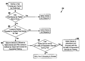
- FIG. 5 illustrates a flowchart showing a process 70 for determining associative grouping for the groups 19 , 22 , and 42 in FIGS. 1-4 , in accordance with embodiments of the present invention.
- a first electrical device e.g., dependent devices 7 or 8
- type of test to be performed e.g., passing a signal (e.g., data) between an input and an output of a SerDes
- step 50 a first electrical device (e.g., dependent devices 7 or 8 ) and type of test to be performed (e.g., passing a signal (e.g., data) between an input and an output of a SerDes) is defined for manufacturing testing. If it is determined in step 52 that the first device may be tested stand alone (i.e., without any other devices) then an alpha device is not required for the manufacturing test.
- a signal e.g., data
- step 56 determines if a second device is required to apply control to the first device for the manufacturing test. If it is determined in step 56 that a second device is not required then an alpha device is not required. If it is determined in step 56 that a second device is required then the second device is defined as an alpha device and the first device is defined as a dependent device. If it is determined in step 62 that the alpha device may control a plurality of dependent devices then in step 64 the alpha device is associated and grouped with the plurality of dependent devices for manufacturing testing. If it is determined in step 62 that the alpha device may not control a plurality of dependent devices then only 1 to 1 grouping is allowed (i.e., only one alpha and one dependent is associatively grouped).
Landscapes
- Engineering & Computer Science (AREA)
- General Engineering & Computer Science (AREA)
- Physics & Mathematics (AREA)
- General Physics & Mathematics (AREA)
- Computer Hardware Design (AREA)
- Computer Networks & Wireless Communication (AREA)
- Semiconductor Integrated Circuits (AREA)
Abstract
A structure and associated method for associated grouping of an alpha device with a plurality of dependent devices for a manufacturing test. The alpha device comprises at least one electrical characteristic. The plurality of dependent devices each comprise the at least one electrical characteristic. The alpha device and the plurality dependent devices are grouped together within a semiconductor device for an associated manufacturing test.
Description
1. Technical Field
The present invention relates to a structure and associated method to associatively group a plurality of cores for a manufacturing test.
2. Related Art
Electrical devices are typically required to operate within design specifications. If an electrical device does not operate within design specifications, the electrical device may malfunction and require replacement which may be costly. Therefore there exists a need to verify that the electrical device is operating within design specifications.
The present invention provides an electrical structure comprising
-
- an alpha device comprising at least one electrical characteristic; and
- a plurality of dependent devices comprising the at least one electrical characteristic, wherein the alpha device and the plurality dependent devices are grouped together within a semiconductor device for an associated manufacturing test.
The present invention provides an a method, comprising:
-
- identifying at least one electrical characteristic for an alpha device;
- identifying the at least one electrical characteristic for a plurality of dependent devices; and
- identifying a group comprising the alpha device and the plurality dependent devices comprising the at least one electrical characteristic for associated manufacturing testing.
The present invention advantageously provides a structure and associated method to associatively verify that an electrical device is operating within design specifications.
Assume for the following test that the alpha devices 4A, 4B, and 4C are each equivalent high speed PLL circuits (i.e. speed (e.g., 8×speed) at which PLL circuit ramps up input frequency ( input signals 12A, 12B, and 12C) to output frequency ( output control signals 16A, 16B, and 16C),). Additionally, each of the plurality of dependent devices 7 is a serializer/deserializer (SerDes) requiring a high frequency signal (i.e., output signal 16A) to operate. The semiconductor device 2 is an ASIC. High frequency is defined herein as a frequency selected from a range of about 1 gigahertz to about 6 gigahertz. The manufacturing test is designed to test that the SerDes will properly operate at a specific frequency (i.e., frequency of output control signal 16A from the PLL circuit (alpha device 4A)). Proper operation of the SerDes includes passing a signal (e.g., data) between an input and an output of the SerDes and at a speed at which the signal is passed between the input and the output of the SerDes. If the SerDes are found to be operational within design tolerances then the manufacturing test is over and each SerDes may be disconnected from the PLL and reconnected to any associated circuitry on the ASIC to perform their intended (i.e., designed) function.
The present invention is a method of associative grouping an alpha device (e.g., alpha device 4A) with associated dependent devices (e.g., the plurality of dependent devices 7) for a manufacturing test. The alpha devices 4A, 4B, and 4C in FIG. 1 are equivalent so any of the alpha devices 4A, 4B, and 4C could have been grouped with the plurality of dependent devices 7 (e.g., alpha devices 4A, 4B, and 4C could be interchanged). Therefore, the method of associated grouping is not required for FIG. 1 since any combination of alpha devices and dependent devices will work. A problem arises when a semiconductor device comprises a plurality of alpha devices each comprising different electrical properties. In this instance the method of associated grouping is required as described in the description of FIG. 2.
Assume for the following test that the alpha devices 6, 4B, and 4C are each high speed PLL circuits (i.e. speed at which PLL circuit ramps up input frequency (input signals 12A, 12B, and 15) to output frequency (output control signals 17, 16B, and 16C)). The alpha device 6 (PLL) comprises a 16×speed while the alpha devices 4B and 4C (PLL) each comprise an 8×speed. Additionally, each of the plurality of dependent devices 8 is a serializer/deserializer (SerDes) requiring a high frequency signal (i.e., output signal 17) to operate. High frequency is defined herein as a frequency selected from a range of about 1 gigahertz to about 6 gigahertz. The semiconductor device 5 is an ASIC. The manufacturing test is designed to test that the SerDes will properly operate at a specific frequency (i.e., frequency of output control signal 17 from the PLL circuit (alpha device 6)). Proper operation of the SerDes includes passing a signal (e.g., data) between an input and an output of the SerDes and a speed at which the signal is passed between the input and the output of the SerDes. If the SerDes are found to be operational within design tolerances then the manufacturing test is over and each SerDes may be disconnected from the PLL and reconnected to any associated circuitry on the ASIC to perform their intended (i.e., designed) function.
The present invention is a method of associative grouping an alpha device (e.g., alpha device 6) with associated dependent devices (e.g., the plurality of dependent devices 8) for a manufacturing test. The alpha devices 4B and 4C in FIG. 2 are not equivalent to the alpha device 6. Only the alpha device 6 is compatible with the plurality of dependent devices 8 so the alpha devices 4B and 4C may not be grouped with the plurality of dependent devices 8 for the manufacturing test (i.e., alpha devices 4B and 4C may not be interchanged with the alpha device 6 for the manufacturing test). Therefore, the method of associated grouping is required for FIG. 2 since only a specific (alpha 6 with dependents 8) group will work.
While embodiments of the present invention have been described herein for purposes of illustration, many modifications and changes will become apparent to those skilled in the art. Accordingly, the appended claims are intended to encompass all such modifications and changes as fall within the true spirit and scope of this invention.
Claims (20)
1. A method, comprising:
identifying at least one electrical characteristic for an alpha device;
identifying the at least one electrical characteristic for a plurality of dependent devices; and
identifying a group comprising the alpha device and the plurality of dependent devices comprising the at least one electrical characteristic for associated manufacturing testing.
2. The method of claim 1 , further comprising grouping the alpha device and the plurality of dependent devices together on a semiconductor device for the associated manufacturing testing.
3. The method of claim 2 , wherein said grouping comprises electrically connecting the alpha device to the plurality of dependent devices during the associated manufacturing testing.
4. The method of claim 3 , further comprising electrically disconnecting the alpha device from the plurality of dependent devices upon completion of the associated manufacturing testing.
5. The method of claim 2 , further comprising providing by the alpha device, a first signal adapted to operate the plurality of dependent devices during the associated manufacturing testing.
6. The method of claim 5 , further comprising providing a second signal adapted to operate the plurality of dependent devices during the associated manufacturing testing; and
multiplexing between the first signal and the second signal during the associated manufacturing testing.
7. The method of claim 2 , further comprising testing the plurality of dependent devices simultaneously in parallel during the associated manufacturing testing.
8. The method of claim 2 , further comprising testing the plurality of dependent devices individually during the associated manufacturing testing.
9. The method of claim 2 , wherein the alpha device and the plurality of dependent devices are cores on the semiconductor device.
10. The method of claim 2 , wherein the semiconductor device is an application specific integrated circuit (ASIC).
11. The method of claim 1 , wherein the at least one electrical characteristic comprises an operational frequency of the plurality of dependent devices.
12. The method of claim 11 , wherein the operational frequency comprises a range of about 1 gigahertz to about 6 gigahertz.
13. The method of claim 1 , wherein the at least one electrical characteristic comprises a jitter tolerance of the plurality of dependent devices.
14. The method of claim 1 , wherein the alpha device comprises a phase lock loop circuit.
15. The method of claim 14 , wherein each of the plurality of dependent devices comprise a serializer/deserializer (SerDes) circuit.
16. The method of claim 1 , wherein the associated manufacturing testing comprises testing the plurality of dependent device for functional operation.
17. The method of claim 16 , wherein the associated manufacturing testing comprises testing the plurality of dependent devices for the functional operation within a design specification.
18. The method of claim 17 , wherein the design specification is a frequency range.
19. The method of claim 17 , wherein the design specification is a speed at which the plurality of dependent devices perform the functional operation.
20. The method of claim 1 , wherein the plurality of dependent devices is selected from the group consisting of an analog to digital convertor, a digital to analog convertor, and a BIST engine.
Priority Applications (1)
| Application Number | Priority Date | Filing Date | Title |
|---|---|---|---|
| US10/707,172 US6882159B1 (en) | 2003-11-25 | 2003-11-25 | Associated grouping of embedded cores for manufacturing test |
Applications Claiming Priority (1)
| Application Number | Priority Date | Filing Date | Title |
|---|---|---|---|
| US10/707,172 US6882159B1 (en) | 2003-11-25 | 2003-11-25 | Associated grouping of embedded cores for manufacturing test |
Publications (1)
| Publication Number | Publication Date |
|---|---|
| US6882159B1 true US6882159B1 (en) | 2005-04-19 |
Family
ID=34435643
Family Applications (1)
| Application Number | Title | Priority Date | Filing Date |
|---|---|---|---|
| US10/707,172 Expired - Fee Related US6882159B1 (en) | 2003-11-25 | 2003-11-25 | Associated grouping of embedded cores for manufacturing test |
Country Status (1)
| Country | Link |
|---|---|
| US (1) | US6882159B1 (en) |
Cited By (3)
| Publication number | Priority date | Publication date | Assignee | Title |
|---|---|---|---|---|
| US20080030386A1 (en) * | 2006-08-03 | 2008-02-07 | Kabushiki Kaisha Toshiba | Integrated circuit, self-test method for the integrated circuit, and optical disc apparatus including the integrated circuit |
| US20100253559A1 (en) * | 2009-02-12 | 2010-10-07 | Qualcomm Incorporated | Methods and apparatus for built in self test of analog-to-digital convertors |
| US7940667B1 (en) * | 2006-09-13 | 2011-05-10 | Pmc-Sierra Us, Inc. | Delay measurements and calibration methods and apparatus for distributed wireless systems |
-
2003
- 2003-11-25 US US10/707,172 patent/US6882159B1/en not_active Expired - Fee Related
Cited By (6)
| Publication number | Priority date | Publication date | Assignee | Title |
|---|---|---|---|---|
| US20080030386A1 (en) * | 2006-08-03 | 2008-02-07 | Kabushiki Kaisha Toshiba | Integrated circuit, self-test method for the integrated circuit, and optical disc apparatus including the integrated circuit |
| US7466253B2 (en) * | 2006-08-03 | 2008-12-16 | Kabushiki Kaisha Toshiba | Integrated circuit, self-test method for the integrated circuit, and optical disc apparatus including the integrated circuit |
| CN101119116B (en) * | 2006-08-03 | 2012-02-29 | 株式会社东芝 | Integrated circuit, self-test method for the integrated circuit, and optical disc apparatus including the integrated circuit |
| US7940667B1 (en) * | 2006-09-13 | 2011-05-10 | Pmc-Sierra Us, Inc. | Delay measurements and calibration methods and apparatus for distributed wireless systems |
| US20100253559A1 (en) * | 2009-02-12 | 2010-10-07 | Qualcomm Incorporated | Methods and apparatus for built in self test of analog-to-digital convertors |
| US8106801B2 (en) | 2009-02-12 | 2012-01-31 | Qualcomm, Incorporated | Methods and apparatus for built in self test of analog-to-digital convertors |
Similar Documents
| Publication | Publication Date | Title |
|---|---|---|
| US7772828B2 (en) | Automatic test equipment capable of high speed test | |
| CN100492043C (en) | Testing method and tester for semiconductor integrated circuit device comprising high-speed input/output element | |
| US9453882B2 (en) | Scan paths with gating, enable, and select decode control circuits | |
| US10877093B2 (en) | Non-interleaved scan operation for achieving higher scan throughput in presence of slower scan outputs | |
| US7810003B2 (en) | Method of generating test clock signal and test clock signal generator for testing semiconductor devices | |
| US8149901B2 (en) | Channel switching circuit | |
| US20040128598A1 (en) | Integrated circuit device including a scan test circuit and methods of testing the same | |
| US20110099443A1 (en) | Test apparatus | |
| US6972592B2 (en) | Self-timed scan circuit for ASIC fault testing | |
| US7882474B2 (en) | Testing phase error of multiple on-die clocks | |
| US7131041B2 (en) | Semiconductor integrated circuit device and device for testing same | |
| US6882159B1 (en) | Associated grouping of embedded cores for manufacturing test | |
| EP4224180B1 (en) | Dft architecture for analog circuits | |
| US10317464B2 (en) | Dynamic scan chain reconfiguration in an integrated circuit | |
| US5132614A (en) | Semiconductor device and method and apparatus for testing the same | |
| US11320485B1 (en) | Scan wrapper architecture for system-on-chip | |
| US20230128466A1 (en) | Automatic test pattern generation circuitry in multi power domain system on a chip | |
| CN101111776A (en) | Semiconductor integrated circuits and system LSIs | |
| US7089471B2 (en) | Scan testing mode control of gated clock signals for flip-flops | |
| US7529294B2 (en) | Testing of multiple asynchronous logic domains | |
| US7644329B2 (en) | Integrated circuit testing method and related circuit thereof | |
| JP4704514B2 (en) | Test equipment | |
| JPH04361179A (en) | Semiconductor integrated circuit device | |
| US20050044461A1 (en) | Semiconductor device test circuit and semiconductor device | |
| US20070132472A1 (en) | Semiconductor integrated circuit and method for testing the same |
Legal Events
| Date | Code | Title | Description |
|---|---|---|---|
| AS | Assignment |
Owner name: INTERNATIONAL BUSINESS MACHINES CORPORATION, NEW Y Free format text: ASSIGNMENT OF ASSIGNORS INTEREST;ASSIGNORS:COWAN, BRUCE;OCKUNZZI, KELLY A.;PRATT, JESSICA H.;AND OTHERS;REEL/FRAME:014153/0743 Effective date: 20031124 |
|
| FEPP | Fee payment procedure |
Free format text: PAYOR NUMBER ASSIGNED (ORIGINAL EVENT CODE: ASPN); ENTITY STATUS OF PATENT OWNER: LARGE ENTITY |
|
| REMI | Maintenance fee reminder mailed | ||
| LAPS | Lapse for failure to pay maintenance fees | ||
| STCH | Information on status: patent discontinuation |
Free format text: PATENT EXPIRED DUE TO NONPAYMENT OF MAINTENANCE FEES UNDER 37 CFR 1.362 |
|
| FP | Lapsed due to failure to pay maintenance fee |
Effective date: 20090419 |