US6869699B2 - P-type materials and mixtures for electronic devices - Google Patents
P-type materials and mixtures for electronic devices Download PDFInfo
- Publication number
- US6869699B2 US6869699B2 US10/391,176 US39117603A US6869699B2 US 6869699 B2 US6869699 B2 US 6869699B2 US 39117603 A US39117603 A US 39117603A US 6869699 B2 US6869699 B2 US 6869699B2
- Authority
- US
- United States
- Prior art keywords
- substituted
- carbon atoms
- heterocyclic
- alkenyl
- aryl
- Prior art date
- Legal status (The legal status is an assumption and is not a legal conclusion. Google has not performed a legal analysis and makes no representation as to the accuracy of the status listed.)
- Expired - Lifetime
Links
- 0 [1*]C1=C2C(=C([4*])C([3*])=C1[2*])N([10*])C1=C([5*])C([6*])=C([7*])C([8*])=C1N2[9*] Chemical compound [1*]C1=C2C(=C([4*])C([3*])=C1[2*])N([10*])C1=C([5*])C([6*])=C([7*])C([8*])=C1N2[9*] 0.000 description 8
- CSEDBXHEBDVFND-XOHWUJONSA-N [C-]#[N+]/C(C#N)=C1/C(C)=C(F)/C(=C(\C#N)[N+]#[C-])C(F)=C1F Chemical compound [C-]#[N+]/C(C#N)=C1/C(C)=C(F)/C(=C(\C#N)[N+]#[C-])C(F)=C1F CSEDBXHEBDVFND-XOHWUJONSA-N 0.000 description 4
- UIIRTMMTFRJUAL-YOPQAMBCSA-N [C-]#[N+]/C(C)=C1/C=C/C2=C/C(=C(\C#N)[N+]#[C-])/C=C\C2=C1 Chemical compound [C-]#[N+]/C(C)=C1/C=C/C2=C/C(=C(\C#N)[N+]#[C-])/C=C\C2=C1 UIIRTMMTFRJUAL-YOPQAMBCSA-N 0.000 description 4
- ORXKFTWMSVAGTL-BASFJDSNSA-N [C-]#[N+]C(C)=C1C=CC(=C(C#N)[N+]#[C-])C=C1 Chemical compound [C-]#[N+]C(C)=C1C=CC(=C(C#N)[N+]#[C-])C=C1 ORXKFTWMSVAGTL-BASFJDSNSA-N 0.000 description 4
- OCGUJKUXPQBXOP-UHFFFAOYSA-N CC1=CC=C(N2C3=CC4=C(C=CC=C4)C=C3N(C3=CC=C(C)C=C3)C3=C/C4=C(C=CC=C4)/C=C\32)C=C1 Chemical compound CC1=CC=C(N2C3=CC4=C(C=CC=C4)C=C3N(C3=CC=C(C)C=C3)C3=C/C4=C(C=CC=C4)/C=C\32)C=C1 OCGUJKUXPQBXOP-UHFFFAOYSA-N 0.000 description 3
- HFXZVYLWHZCRCV-UHFFFAOYSA-N C/C1=C2C(=C\C3=C1C=CC=C3)/N(C1=CC=CC=C1)C1=CC3=C(C=CC=C3)C=C1N/2C1=CC=CC=C1 Chemical compound C/C1=C2C(=C\C3=C1C=CC=C3)/N(C1=CC=CC=C1)C1=CC3=C(C=CC=C3)C=C1N/2C1=CC=CC=C1 HFXZVYLWHZCRCV-UHFFFAOYSA-N 0.000 description 2
- WWEKUYXKPHWHFU-UHFFFAOYSA-N C1=CC2=CC=C(N3C4=CC5=C(C=CC=C5)C=C4N(C4=CC=C5C=CC=CC5=C4)C4=C/C5=C(C=CC=C5)/C=C\43)C=C2C=C1 Chemical compound C1=CC2=CC=C(N3C4=CC5=C(C=CC=C5)C=C4N(C4=CC=C5C=CC=CC5=C4)C4=C/C5=C(C=CC=C5)/C=C\43)C=C2C=C1 WWEKUYXKPHWHFU-UHFFFAOYSA-N 0.000 description 2
- FYKAJULMKNDLPN-UHFFFAOYSA-N C1=CC2=CC=C(N3C4=CC=C5CCCCC5=C4N(C4=CC=C5C=CC=CC5=C4)C4=C/C5=C(C=CC=C5)/C=C\43)C=C2C=C1 Chemical compound C1=CC2=CC=C(N3C4=CC=C5CCCCC5=C4N(C4=CC=C5C=CC=CC5=C4)C4=C/C5=C(C=CC=C5)/C=C\43)C=C2C=C1 FYKAJULMKNDLPN-UHFFFAOYSA-N 0.000 description 2
- MVIAIRWBQZSDIS-UHFFFAOYSA-N C1=CC=C(C(=CN2C3=CC=CC=C3N(C=C(C3=CC=CC=C3)C3=CC=CC=C3)C3=CC4=C(C=CC=C4)C=C32)C2=CC=CC=C2)C=C1 Chemical compound C1=CC=C(C(=CN2C3=CC=CC=C3N(C=C(C3=CC=CC=C3)C3=CC=CC=C3)C3=CC4=C(C=CC=C4)C=C32)C2=CC=CC=C2)C=C1 MVIAIRWBQZSDIS-UHFFFAOYSA-N 0.000 description 2
- ZOWTXWJDUWWDGF-UHFFFAOYSA-N C1=CC=C(C2=CC=C(N3C4=CC=C5CCCCC5=C4N(C4=CC=C(C5=CC=CC=C5)C=C4)C4=CC=C5CCCCC5=C43)C=C2)C=C1 Chemical compound C1=CC=C(C2=CC=C(N3C4=CC=C5CCCCC5=C4N(C4=CC=C(C5=CC=CC=C5)C=C4)C4=CC=C5CCCCC5=C43)C=C2)C=C1 ZOWTXWJDUWWDGF-UHFFFAOYSA-N 0.000 description 2
- JEWPDHFEKOGELQ-UHFFFAOYSA-N C1=CC=C(C2=CC=C(N3C4=CC=CC=C4N(C4=CC=C(C5=CC=CC=C5)C=C4)C4=C/C5=C(C=CC=C5)/C=C\43)C=C2)C=C1 Chemical compound C1=CC=C(C2=CC=C(N3C4=CC=CC=C4N(C4=CC=C(C5=CC=CC=C5)C=C4)C4=C/C5=C(C=CC=C5)/C=C\43)C=C2)C=C1 JEWPDHFEKOGELQ-UHFFFAOYSA-N 0.000 description 2
- VMCIUWUJCIMOFV-UHFFFAOYSA-N CC1=C(C)C=C2C(=C1)N(C1=CC=C3C=CC=CC3=C1)C1=C/C3=C(C=CC=C3)/C=C\1N2C1=CC=C2C=CC=CC2=C1 Chemical compound CC1=C(C)C=C2C(=C1)N(C1=CC=C3C=CC=CC3=C1)C1=C/C3=C(C=CC=C3)/C=C\1N2C1=CC=C2C=CC=CC2=C1 VMCIUWUJCIMOFV-UHFFFAOYSA-N 0.000 description 2
- ICERBMWHHUSSSU-UHFFFAOYSA-N CC1=C2C(=CC=C1)N(C1=CC=CC=C1)C1=CC3=C(C=CC=C3)C=C1N2C1=CC=CC=C1 Chemical compound CC1=C2C(=CC=C1)N(C1=CC=CC=C1)C1=CC3=C(C=CC=C3)C=C1N2C1=CC=CC=C1 ICERBMWHHUSSSU-UHFFFAOYSA-N 0.000 description 2
- IMVALJHCXWFQFN-UHFFFAOYSA-N CC1=CC=C(N2C3=CC(OC4=CC=CC=C4)=C(OC4=CC=CC=C4)C=C3N(C3=CC=C(C)C=C3)C3=C/C4=C(C=CC=C4)/C=C\32)C=C1 Chemical compound CC1=CC=C(N2C3=CC(OC4=CC=CC=C4)=C(OC4=CC=CC=C4)C=C3N(C3=CC=C(C)C=C3)C3=C/C4=C(C=CC=C4)/C=C\32)C=C1 IMVALJHCXWFQFN-UHFFFAOYSA-N 0.000 description 2
- NAMSQXVRWRUWGH-UHFFFAOYSA-N CC1=CC=C(N2C3=CC4=C(C=C3N(C3=CC=C(C)C=C3)C3=C2/C=C2/C=CC=C/C2=C/3)CCCC4)C=C1 Chemical compound CC1=CC=C(N2C3=CC4=C(C=C3N(C3=CC=C(C)C=C3)C3=C2/C=C2/C=CC=C/C2=C/3)CCCC4)C=C1 NAMSQXVRWRUWGH-UHFFFAOYSA-N 0.000 description 2
- QRGDKKRLLKUFIS-UHFFFAOYSA-N CC1=CC=C(N2C3=CC=C(C4=CC=NC=C4)C=C3N(C3=CC=C(C)C=C3)C3=C/C4=C(C=CC=C4)/C=C\32)C=C1 Chemical compound CC1=CC=C(N2C3=CC=C(C4=CC=NC=C4)C=C3N(C3=CC=C(C)C=C3)C3=C/C4=C(C=CC=C4)/C=C\32)C=C1 QRGDKKRLLKUFIS-UHFFFAOYSA-N 0.000 description 2
- WTIYUTVPMQQGFG-UHFFFAOYSA-N CC1=CC=C(N2C3=CC=CC=C3N(C3=CC=C(C)C=C3)C3=C/C4=C(C=CC=C4)/C=C\32)C=C1 Chemical compound CC1=CC=C(N2C3=CC=CC=C3N(C3=CC=C(C)C=C3)C3=C/C4=C(C=CC=C4)/C=C\32)C=C1 WTIYUTVPMQQGFG-UHFFFAOYSA-N 0.000 description 2
- DILJMKAVCOFHCV-UHFFFAOYSA-N COC1=CC2=CC=C(N3C4=CC(C)=C(C)C=C4N(C4=CC=C5C=C(OC)C=CC5=C4)C4=C/C5=C(C=CC=C5)/C=C\43)C=C2C=C1 Chemical compound COC1=CC2=CC=C(N3C4=CC(C)=C(C)C=C4N(C4=CC=C5C=C(OC)C=CC5=C4)C4=C/C5=C(C=CC=C5)/C=C\43)C=C2C=C1 DILJMKAVCOFHCV-UHFFFAOYSA-N 0.000 description 2
- YKVARNRDQMWGIV-UHFFFAOYSA-N C.C1=CC2=NC3=C(C=CC=C3)N=C2C=C1.CC(C)(C)O[Na].CC1=CC(N)=C(N)C=C1C.CCO.NC1=C(N)C=C2C=CC=CC2=C1.NC1=C(N)C=CC=C1.OC1=CC2=C(C=CC=C2)C=C1O.OC1=CC2=C(C=CC=C2)C=C1O.OC1=CC2=C(C=CC=C2)C=C1O.[Ar]Br.[H]N1C2=CC(C)=C(C)C=C2N([H])C2=CC3=C(C=CC=C3)C=C21.[H]N1C2=CC3=C(C=CC=C3)C=C2N([H])C2=CC3=C(C=CC=C3)C=C21.[H]N1C2=CC=CC=C2N([H])C2=CC3=C(C=CC=C3)C=C21.[H]N1C2=CC=CC=C2N([H])C2=CC=CC=C21.[V][I-]I Chemical compound C.C1=CC2=NC3=C(C=CC=C3)N=C2C=C1.CC(C)(C)O[Na].CC1=CC(N)=C(N)C=C1C.CCO.NC1=C(N)C=C2C=CC=CC2=C1.NC1=C(N)C=CC=C1.OC1=CC2=C(C=CC=C2)C=C1O.OC1=CC2=C(C=CC=C2)C=C1O.OC1=CC2=C(C=CC=C2)C=C1O.[Ar]Br.[H]N1C2=CC(C)=C(C)C=C2N([H])C2=CC3=C(C=CC=C3)C=C21.[H]N1C2=CC3=C(C=CC=C3)C=C2N([H])C2=CC3=C(C=CC=C3)C=C21.[H]N1C2=CC=CC=C2N([H])C2=CC3=C(C=CC=C3)C=C21.[H]N1C2=CC=CC=C2N([H])C2=CC=CC=C21.[V][I-]I YKVARNRDQMWGIV-UHFFFAOYSA-N 0.000 description 1
- INGSONROEHHCJP-UHFFFAOYSA-N C/C1=C2C(=C\C3=C1C=CC=C3)/N(C1=CC=C3C=CC=CC3=C1)C1=CC3=C(C=CC=C3)C=C1N/2C1=CC=C2C=CC=CC2=C1 Chemical compound C/C1=C2C(=C\C3=C1C=CC=C3)/N(C1=CC=C3C=CC=CC3=C1)C1=CC3=C(C=CC=C3)C=C1N/2C1=CC=C2C=CC=CC2=C1 INGSONROEHHCJP-UHFFFAOYSA-N 0.000 description 1
- KRIPYKVZDXWCFP-UHFFFAOYSA-N C1=CC2=C(C=C1)C=C(N1C3=CC=C(C4CCCCC4)C=C3N(C3=CC4=C(C=CC=C4)C=C3)C3=C/C4=C(C=CC=C4)/C=C\31)C=C2 Chemical compound C1=CC2=C(C=C1)C=C(N1C3=CC=C(C4CCCCC4)C=C3N(C3=CC4=C(C=CC=C4)C=C3)C3=C/C4=C(C=CC=C4)/C=C\31)C=C2 KRIPYKVZDXWCFP-UHFFFAOYSA-N 0.000 description 1
- KUVUCVICXJGVIH-UHFFFAOYSA-N C1=CC2=C(C=C1)C=C1C(=C2)N(C2=CC3=C(C=C2)OC=C3)C2=CC3=C(C=CC=C3)C=C2N1C1=CC2=C(C=C1)OC=C2 Chemical compound C1=CC2=C(C=C1)C=C1C(=C2)N(C2=CC3=C(C=C2)OC=C3)C2=CC3=C(C=CC=C3)C=C2N1C1=CC2=C(C=C1)OC=C2 KUVUCVICXJGVIH-UHFFFAOYSA-N 0.000 description 1
- OEUFSDRSMDNGQA-UHFFFAOYSA-N C1=CC2=C(C=C1)C=C1C(=C2)N(C2=CC3=C(C=C2)SC=C3)C2=CC3=C(C=CC=C3)C=C2N1C1=CC2=C(C=C1)SC=C2 Chemical compound C1=CC2=C(C=C1)C=C1C(=C2)N(C2=CC3=C(C=C2)SC=C3)C2=CC3=C(C=CC=C3)C=C2N1C1=CC2=C(C=C1)SC=C2 OEUFSDRSMDNGQA-UHFFFAOYSA-N 0.000 description 1
- CXNAOKKQJLRYPI-UHFFFAOYSA-N C1=CC2=C(C=C1)C=C1C(=C2)N(C2CCCCC2)C2=CC3=C(C=CC=C3)C=C2N1C1CCCCC1 Chemical compound C1=CC2=C(C=C1)C=C1C(=C2)N(C2CCCCC2)C2=CC3=C(C=CC=C3)C=C2N1C1CCCCC1 CXNAOKKQJLRYPI-UHFFFAOYSA-N 0.000 description 1
- QBPUNKYGNLINPW-UHFFFAOYSA-N C1=CC2=C(C=C1)C=C1C(=C2)N(C2CCOCC2)C2=CC3=C(C=CC=C3)C=C2N1C1CCOCC1 Chemical compound C1=CC2=C(C=C1)C=C1C(=C2)N(C2CCOCC2)C2=CC3=C(C=CC=C3)C=C2N1C1CCOCC1 QBPUNKYGNLINPW-UHFFFAOYSA-N 0.000 description 1
- INDZSRAUYROONA-UHFFFAOYSA-N C1=CC2=CC=C(N3C4=CC5=C(C=C4N(C4=CC=C6C=CC=CC6=C4)C4=C3/C=C3/C=CC=C/C3=C/4)CCC5)C=C2C=C1 Chemical compound C1=CC2=CC=C(N3C4=CC5=C(C=C4N(C4=CC=C6C=CC=CC6=C4)C4=C3/C=C3/C=CC=C/C3=C/4)CCC5)C=C2C=C1 INDZSRAUYROONA-UHFFFAOYSA-N 0.000 description 1
- WWAQJVZXWLAGMU-UHFFFAOYSA-N C1=CC2=CC=C(N3C4=CC5=C(C=C4N(C4=CC=C6C=CC=CC6=C4)C4=C3/C=C3/C=CC=C/C3=C/4)CCCC5)C=C2C=C1 Chemical compound C1=CC2=CC=C(N3C4=CC5=C(C=C4N(C4=CC=C6C=CC=CC6=C4)C4=C3/C=C3/C=CC=C/C3=C/4)CCCC5)C=C2C=C1 WWAQJVZXWLAGMU-UHFFFAOYSA-N 0.000 description 1
- KCFCYUJOMWKNLA-UHFFFAOYSA-N C1=CC2=CC=C(N3C4=CC5=C(C=C4N(C4=CC=C6C=CC=CC6=C4)C4=C3/C=C3/C=CC=C/C3=C/4)OCCO5)C=C2C=C1 Chemical compound C1=CC2=CC=C(N3C4=CC5=C(C=C4N(C4=CC=C6C=CC=CC6=C4)C4=C3/C=C3/C=CC=C/C3=C/4)OCCO5)C=C2C=C1 KCFCYUJOMWKNLA-UHFFFAOYSA-N 0.000 description 1
- CRNRWOMSZZQQQL-UHFFFAOYSA-N C1=CC=C(C(=CC2=CC=C3C(=C2)N(C2=CC=C4C=CC=CC4=C2)C2=C/C4=C(C=CC=C4)/C=C\2N3C2=CC=C3C=CC=CC3=C2)C2=CC=CC=C2)C=C1 Chemical compound C1=CC=C(C(=CC2=CC=C3C(=C2)N(C2=CC=C4C=CC=CC4=C2)C2=C/C4=C(C=CC=C4)/C=C\2N3C2=CC=C3C=CC=CC3=C2)C2=CC=CC=C2)C=C1 CRNRWOMSZZQQQL-UHFFFAOYSA-N 0.000 description 1
- QYWHZULZCVCFFA-UHFFFAOYSA-N C1=CC=C(C2=CC=C(N3C4=CC5=C(C=CC=C5)C=C4N(C4=CC=C(C5=CC=CC=C5)C=C4)C4=C/C5=C(C=CC=C5)/C=C\43)C=C2)C=C1 Chemical compound C1=CC=C(C2=CC=C(N3C4=CC5=C(C=CC=C5)C=C4N(C4=CC=C(C5=CC=CC=C5)C=C4)C4=C/C5=C(C=CC=C5)/C=C\43)C=C2)C=C1 QYWHZULZCVCFFA-UHFFFAOYSA-N 0.000 description 1
- GZCAXZKAYYMECF-UHFFFAOYSA-N C1=CC=C(C2=CC=C(N3C4=CC=C(C5CCCCC5)C=C4N(C4=CC=C(C5=CC=CC=C5)C=C4)C4=C/C5=C(C=CC=C5)/C=C\43)C=C2)C=C1 Chemical compound C1=CC=C(C2=CC=C(N3C4=CC=C(C5CCCCC5)C=C4N(C4=CC=C(C5=CC=CC=C5)C=C4)C4=C/C5=C(C=CC=C5)/C=C\43)C=C2)C=C1 GZCAXZKAYYMECF-UHFFFAOYSA-N 0.000 description 1
- JYAHUZDTVPRXEP-UHFFFAOYSA-N C1=CC=C(C2=CC=C(N3C4=CC=C5C=CC=CC5=C4N(C4=CC=C(C5=CC=CC=C5)C=C4)C4=CC=C5C=CC=CC5=C43)C=C2)C=C1 Chemical compound C1=CC=C(C2=CC=C(N3C4=CC=C5C=CC=CC5=C4N(C4=CC=C(C5=CC=CC=C5)C=C4)C4=CC=C5C=CC=CC5=C43)C=C2)C=C1 JYAHUZDTVPRXEP-UHFFFAOYSA-N 0.000 description 1
- CNIPZBVWCQDMPS-UHFFFAOYSA-N C1=CC=C(N(C2=CC=CC=C2)C2=CC=C(C3=CC=C4C(=C3)N(C3=CC=CC=C3)C3=C/C5=C(C=CC=C5)/C=C\3N4C3=CC=CC=C3)C=C2)C=C1 Chemical compound C1=CC=C(N(C2=CC=CC=C2)C2=CC=C(C3=CC=C4C(=C3)N(C3=CC=CC=C3)C3=C/C5=C(C=CC=C5)/C=C\3N4C3=CC=CC=C3)C=C2)C=C1 CNIPZBVWCQDMPS-UHFFFAOYSA-N 0.000 description 1
- HMXVTAWVTKBDQL-UHFFFAOYSA-N C1=CC=C(N(C2=CC=CC=C2)C2=CC=C3C(=C2)N(C2=CC=C4C=CC=CC4=C2)C2=C/C4=C(C=CC=C4)/C=C\2N3C2=CC=C3C=CC=CC3=C2)C=C1 Chemical compound C1=CC=C(N(C2=CC=CC=C2)C2=CC=C3C(=C2)N(C2=CC=C4C=CC=CC4=C2)C2=C/C4=C(C=CC=C4)/C=C\2N3C2=CC=C3C=CC=CC3=C2)C=C1 HMXVTAWVTKBDQL-UHFFFAOYSA-N 0.000 description 1
- VDQQAMISCOWZTC-UHFFFAOYSA-N C1=CC=C(N2C3=CC4=C(C=CC=C4)C=C3N(C3=CC=CC=C3)C3=C4\C=CC=C\C4=C\C=C\32)C=C1 Chemical compound C1=CC=C(N2C3=CC4=C(C=CC=C4)C=C3N(C3=CC=CC=C3)C3=C4\C=CC=C\C4=C\C=C\32)C=C1 VDQQAMISCOWZTC-UHFFFAOYSA-N 0.000 description 1
- PZTBHKLLOBBDJO-UHFFFAOYSA-N C1=CC=C2C(=C1)N(C1=CC=C3C=CC=CC3=C1)C1=C/C3=C(C=CC=C3)/C=C\1N2C1=CC=C2C=CC=CC2=C1 Chemical compound C1=CC=C2C(=C1)N(C1=CC=C3C=CC=CC3=C1)C1=C/C3=C(C=CC=C3)/C=C\1N2C1=CC=C2C=CC=CC2=C1 PZTBHKLLOBBDJO-UHFFFAOYSA-N 0.000 description 1
- HPIOBCHPZVAATK-UHFFFAOYSA-N C1=CC=C2C(=C1)N(C1=CC=C3C=CC=CC3=C1)C1=C/C=C/C=C\1N2C1=CC=C2C=CC=CC2=C1 Chemical compound C1=CC=C2C(=C1)N(C1=CC=C3C=CC=CC3=C1)C1=C/C=C/C=C\1N2C1=CC=C2C=CC=CC2=C1 HPIOBCHPZVAATK-UHFFFAOYSA-N 0.000 description 1
- RZNCOQQBYUUJAW-UHFFFAOYSA-N CC1(C)CCC(C)(C)C2=C1C=C1C(=C2)N(C2=CC=C(C3=CC=CC=C3)C=C2)C2=C(/C=C3/C=CC=C/C3=C/2)N1C1=CC=C(C2=CC=CC=C2)C=C1 Chemical compound CC1(C)CCC(C)(C)C2=C1C=C1C(=C2)N(C2=CC=C(C3=CC=CC=C3)C=C2)C2=C(/C=C3/C=CC=C/C3=C/2)N1C1=CC=C(C2=CC=CC=C2)C=C1 RZNCOQQBYUUJAW-UHFFFAOYSA-N 0.000 description 1
- NGTOBWXESAIIJN-UHFFFAOYSA-N CC1(C)CCC(C)(C)C2=C1C=C1C(=C2)N(C2=CC=C3C=CC=CC3=C2)C2=C/C3=C(C=CC=C3)/C=C\2N1C1=CC=C2C=CC=CC2=C1 Chemical compound CC1(C)CCC(C)(C)C2=C1C=C1C(=C2)N(C2=CC=C3C=CC=CC3=C2)C2=C/C3=C(C=CC=C3)/C=C\2N1C1=CC=C2C=CC=CC2=C1 NGTOBWXESAIIJN-UHFFFAOYSA-N 0.000 description 1
- FPYIVXDZWWYCAW-UHFFFAOYSA-N CC1(C)OC2=C(C=C3C(=C2)N(C2=CC=C4C=CC=CC4=C2)C2=C(/C=C4/C=CC=C/C4=C/2)N3C2=CC=C3C=CC=CC3=C2)O1 Chemical compound CC1(C)OC2=C(C=C3C(=C2)N(C2=CC=C4C=CC=CC4=C2)C2=C(/C=C4/C=CC=C/C4=C/2)N3C2=CC=C3C=CC=CC3=C2)O1 FPYIVXDZWWYCAW-UHFFFAOYSA-N 0.000 description 1
- IDSRVCNQUKZCBJ-UHFFFAOYSA-N CC1=C(C)/C=C2C(=C/1)\N(C1=CC=C3C=CC=CC3=C1)C1=CC=C3C=CC=CC3=C1N\2C1=CC=C2C=CC=CC2=C1 Chemical compound CC1=C(C)/C=C2C(=C/1)\N(C1=CC=C3C=CC=CC3=C1)C1=CC=C3C=CC=CC3=C1N\2C1=CC=C2C=CC=CC2=C1 IDSRVCNQUKZCBJ-UHFFFAOYSA-N 0.000 description 1
- NIKVDGXXXMMIFJ-LTTYKRRRSA-N CC1=C(C)C=C2C(=C1)N(/C=C/C=C(C1=CC=CC=C1)C1=CC=CC=C1)C1=CC3=C(C=CC=C3)C=C1N2/C=C/C=C(C1=CC=CC=C1)C1=CC=CC=C1 Chemical compound CC1=C(C)C=C2C(=C1)N(/C=C/C=C(C1=CC=CC=C1)C1=CC=CC=C1)C1=CC3=C(C=CC=C3)C=C1N2/C=C/C=C(C1=CC=CC=C1)C1=CC=CC=C1 NIKVDGXXXMMIFJ-LTTYKRRRSA-N 0.000 description 1
- SQGVWUSWLOYCBA-UHFFFAOYSA-N CC1=C(C)C=C2C(=C1)N(C1=CC3=C(C=C1)OC=C3)C1=CC3=C(C=CC=C3)C=C1N2C1=CC2=C(C=C1)OC=C2 Chemical compound CC1=C(C)C=C2C(=C1)N(C1=CC3=C(C=C1)OC=C3)C1=CC3=C(C=CC=C3)C=C1N2C1=CC2=C(C=C1)OC=C2 SQGVWUSWLOYCBA-UHFFFAOYSA-N 0.000 description 1
- QEEKDBXGVLWBMY-UHFFFAOYSA-N CC1=C(C)C=C2C(=C1)N(C1=CC3=C(C=C1)SC=C3)C1=CC3=C(C=CC=C3)C=C1N2C1=CC2=C(C=C1)SC=C2 Chemical compound CC1=C(C)C=C2C(=C1)N(C1=CC3=C(C=C1)SC=C3)C1=CC3=C(C=CC=C3)C=C1N2C1=CC2=C(C=C1)SC=C2 QEEKDBXGVLWBMY-UHFFFAOYSA-N 0.000 description 1
- GQZLOMMZWDHAOM-UHFFFAOYSA-N CC1=C(C)C=C2C(=C1)N(C1=CC=C(C3=CC=CC=C3)C=C1)C1=C/C3=C(C=CC=C3)/C=C\1N2C1=CC=C(C2=CC=CC=C2)C=C1 Chemical compound CC1=C(C)C=C2C(=C1)N(C1=CC=C(C3=CC=CC=C3)C=C1)C1=C/C3=C(C=CC=C3)/C=C\1N2C1=CC=C(C2=CC=CC=C2)C=C1 GQZLOMMZWDHAOM-UHFFFAOYSA-N 0.000 description 1
- HSVHQWAUTKRTKQ-UHFFFAOYSA-N CC1=C(C)C=C2C(=C1)N(C1=CC=C(N(C3=CC=CC=C3)C3=CC=C4C=CC=CC4=C3)C=C1)C1=C/C3=C(C=CC=C3)/C=C\1N2C1=CC=C(N(C2=CC=CC=C2)C2=CC3=C(C=CC=C3)C=C2)C=C1 Chemical compound CC1=C(C)C=C2C(=C1)N(C1=CC=C(N(C3=CC=CC=C3)C3=CC=C4C=CC=CC4=C3)C=C1)C1=C/C3=C(C=CC=C3)/C=C\1N2C1=CC=C(N(C2=CC=CC=C2)C2=CC3=C(C=CC=C3)C=C2)C=C1 HSVHQWAUTKRTKQ-UHFFFAOYSA-N 0.000 description 1
- QNXGXOWTYIXFLT-UHFFFAOYSA-N CC1=C(C)C=C2C(=C1)N(C1CCCCC1)C1=CC3=C(C=CC=C3)C=C1N2C1CCCCC1 Chemical compound CC1=C(C)C=C2C(=C1)N(C1CCCCC1)C1=CC3=C(C=CC=C3)C=C1N2C1CCCCC1 QNXGXOWTYIXFLT-UHFFFAOYSA-N 0.000 description 1
- ONHRIGNYPFMAMR-UHFFFAOYSA-N CC1=C(C)C=C2C(=C1)N(C1CCOCC1)C1=CC3=C(C=CC=C3)C=C1N2C1CCOCC1 Chemical compound CC1=C(C)C=C2C(=C1)N(C1CCOCC1)C1=CC3=C(C=CC=C3)C=C1N2C1CCOCC1 ONHRIGNYPFMAMR-UHFFFAOYSA-N 0.000 description 1
- RTDDQRIEQBHOQW-UHFFFAOYSA-N CC1=C2C(=C/C=C/1)/N(C1=CC=C3C=CC=CC3=C1)C1=CC3=C(C=CC=C3)C=C1N/2C1=CC=C2C=CC=CC2=C1 Chemical compound CC1=C2C(=C/C=C/1)/N(C1=CC=C3C=CC=CC3=C1)C1=CC3=C(C=CC=C3)C=C1N/2C1=CC=C2C=CC=CC2=C1 RTDDQRIEQBHOQW-UHFFFAOYSA-N 0.000 description 1
- XTPUVGKATXNGBP-UHFFFAOYSA-N CC1=C2C(=C/C=C/1)/N(C1=CC=C3C=CC=CC3=C1)C1=CC=CC=C1N/2C1=CC=C2C=CC=CC2=C1 Chemical compound CC1=C2C(=C/C=C/1)/N(C1=CC=C3C=CC=CC3=C1)C1=CC=CC=C1N/2C1=CC=C2C=CC=CC2=C1 XTPUVGKATXNGBP-UHFFFAOYSA-N 0.000 description 1
- FDBPLYNXYMKTCU-UHFFFAOYSA-N CC1=C2C(=C3C=CC=CC3=C1)N(C)C1=C(C)C=C3C=CC=CC3=C1N2C Chemical compound CC1=C2C(=C3C=CC=CC3=C1)N(C)C1=C(C)C=C3C=CC=CC3=C1N2C FDBPLYNXYMKTCU-UHFFFAOYSA-N 0.000 description 1
- UJCPVAPMRNTXFC-UHFFFAOYSA-N CC1=C2C(=CC3=C1C=CC=C3)N(C1=CC=C(C3=CC=CC=C3)C=C1)C1=C(\C)C3=C(C=CC=C3)/C=C\1N2C1=CC=C(C2=CC=CC=C2)C=C1 Chemical compound CC1=C2C(=CC3=C1C=CC=C3)N(C1=CC=C(C3=CC=CC=C3)C=C1)C1=C(\C)C3=C(C=CC=C3)/C=C\1N2C1=CC=C(C2=CC=CC=C2)C=C1 UJCPVAPMRNTXFC-UHFFFAOYSA-N 0.000 description 1
- GXKHXXNATGTOHH-UHFFFAOYSA-N CC1=C2C(=CC=C1)N(C1=CC=C3C=CC=CC3=C1)C1=C/C(C)=C\C=C\1N2C1=CC=C2C=CC=CC2=C1 Chemical compound CC1=C2C(=CC=C1)N(C1=CC=C3C=CC=CC3=C1)C1=C/C(C)=C\C=C\1N2C1=CC=C2C=CC=CC2=C1 GXKHXXNATGTOHH-UHFFFAOYSA-N 0.000 description 1
- PKVNDKTVOKVERX-UHFFFAOYSA-N CC1=CC(C)=C(C2=CC=C(N3C4=C5C=CSC5=CC=C4N(C4=CC=C(C5=C(C)C=C(C)C=C5C)C=C4)C4=C5\C=CS\C5=C\C=C\43)C=C2)C(C)=C1 Chemical compound CC1=CC(C)=C(C2=CC=C(N3C4=C5C=CSC5=CC=C4N(C4=CC=C(C5=C(C)C=C(C)C=C5C)C=C4)C4=C5\C=CS\C5=C\C=C\43)C=C2)C(C)=C1 PKVNDKTVOKVERX-UHFFFAOYSA-N 0.000 description 1
- CVASPJLRIVPBBQ-UHFFFAOYSA-N CC1=CC(C)=CC(N2C3=CC4=C(C=CC=C4)C=C3N(C3=CC(C)=CC(C)=C3)C3=CC(C4=CC=CC=C4)=C(C4=CC=CC=C4)C=C32)=C1 Chemical compound CC1=CC(C)=CC(N2C3=CC4=C(C=CC=C4)C=C3N(C3=CC(C)=CC(C)=C3)C3=CC(C4=CC=CC=C4)=C(C4=CC=CC=C4)C=C32)=C1 CVASPJLRIVPBBQ-UHFFFAOYSA-N 0.000 description 1
- KERFAKFMHKETQT-UHFFFAOYSA-N CC1=CC(C2=C3C(=CC=C2)N(C)C2=C(\C4=CC(C)=NC(C)=C4)C4=C(C=CC=C4)/C=C\2N3C)=CC(C)=N1 Chemical compound CC1=CC(C2=C3C(=CC=C2)N(C)C2=C(\C4=CC(C)=NC(C)=C4)C4=C(C=CC=C4)/C=C\2N3C)=CC(C)=N1 KERFAKFMHKETQT-UHFFFAOYSA-N 0.000 description 1
- DOAADFZUWZHVQI-UHFFFAOYSA-N CC1=CC2=C(C=C1C)/C=C1C(=C/2)\N(C2=CC=C3C=CC=CC3=C2)C2=CC=C(OC3=CC=CC=C3)C=C2N\1C1=CC=C2C=CC=CC2=C1 Chemical compound CC1=CC2=C(C=C1C)/C=C1C(=C/2)\N(C2=CC=C3C=CC=CC3=C2)C2=CC=C(OC3=CC=CC=C3)C=C2N\1C1=CC=C2C=CC=CC2=C1 DOAADFZUWZHVQI-UHFFFAOYSA-N 0.000 description 1
- RPTUXOAJEMOKGI-UHFFFAOYSA-N CC1=CC=C(C2=C(C3=CC=C(C)C=C3)C=C3C(=C2)N(C2=CC=C(C)C=C2)C2=CC4=C(C=CC=C4)C=C2N3C2=CC=C(C)C=C2)C=C1 Chemical compound CC1=CC=C(C2=C(C3=CC=C(C)C=C3)C=C3C(=C2)N(C2=CC=C(C)C=C2)C2=CC4=C(C=CC=C4)C=C2N3C2=CC=C(C)C=C2)C=C1 RPTUXOAJEMOKGI-UHFFFAOYSA-N 0.000 description 1
- PEBJEZNVSCHCAX-UHFFFAOYSA-N CC1=CC=C(C2=C(C3=CC=C(C)C=C3)C=C3C(=C2)N(C2=CC=C4C=CC=CC4=C2)C2=CC4=C(C=CC=C4)C=C2N3C2=CC=C3C=CC=CC3=C2)C=C1 Chemical compound CC1=CC=C(C2=C(C3=CC=C(C)C=C3)C=C3C(=C2)N(C2=CC=C4C=CC=CC4=C2)C2=CC4=C(C=CC=C4)C=C2N3C2=CC=C3C=CC=CC3=C2)C=C1 PEBJEZNVSCHCAX-UHFFFAOYSA-N 0.000 description 1
- GGQREONKTPMZPT-UHFFFAOYSA-N CC1=CC=C(N(C2=CC=C(C)C=C2)C2=CC=C(N3C4=CC(C)=C(C)C=C4N(C4=CC=C(N(C5=CC=C(C)C=C5)C5=CC=C(C)C=C5)C=C4)C4=C/C5=C(C=CC=C5)/C=C\43)C=C2)C=C1 Chemical compound CC1=CC=C(N(C2=CC=C(C)C=C2)C2=CC=C(N3C4=CC(C)=C(C)C=C4N(C4=CC=C(N(C5=CC=C(C)C=C5)C5=CC=C(C)C=C5)C=C4)C4=C/C5=C(C=CC=C5)/C=C\43)C=C2)C=C1 GGQREONKTPMZPT-UHFFFAOYSA-N 0.000 description 1
- HPPHNWGCMUNEAF-UHFFFAOYSA-N CC1=CC=C(N2C3=CC(C)=C(C)C=C3N(C3=CC=C(C)C=C3)C3=C/C4=C(C=CC=C4)/C=C\32)C=C1 Chemical compound CC1=CC=C(N2C3=CC(C)=C(C)C=C3N(C3=CC=C(C)C=C3)C3=C/C4=C(C=CC=C4)/C=C\32)C=C1 HPPHNWGCMUNEAF-UHFFFAOYSA-N 0.000 description 1
- PRLGOBWRRODWHY-UHFFFAOYSA-N CC1=CC=C(N2C3=CC(SC4=CC=CC=C4)=C(SC4=CC=CC=C4)C=C3N(C3=CC=C(C)C=C3)C3=C/C4=C(C=CC=C4)/C=C\32)C=C1 Chemical compound CC1=CC=C(N2C3=CC(SC4=CC=CC=C4)=C(SC4=CC=CC=C4)C=C3N(C3=CC=C(C)C=C3)C3=C/C4=C(C=CC=C4)/C=C\32)C=C1 PRLGOBWRRODWHY-UHFFFAOYSA-N 0.000 description 1
- YOMREWMAZKWTOJ-UHFFFAOYSA-N CC1=CC=C(N2C3=CC4=C(C=C3N(C3=CC=C(C)C=C3)C3=C2/C=C2/C=CC=C/C2=C/3)C(C)(C)CCC4(C)C)C=C1 Chemical compound CC1=CC=C(N2C3=CC4=C(C=C3N(C3=CC=C(C)C=C3)C3=C2/C=C2/C=CC=C/C2=C/3)C(C)(C)CCC4(C)C)C=C1 YOMREWMAZKWTOJ-UHFFFAOYSA-N 0.000 description 1
- FJZTWCMOVQPEJS-UHFFFAOYSA-N CC1=CC=C(N2C3=CC4=C(C=C3N(C3=CC=C(C)C=C3)C3=C2/C=C2/C=CC=C/C2=C/3)CCC4)C=C1 Chemical compound CC1=CC=C(N2C3=CC4=C(C=C3N(C3=CC=C(C)C=C3)C3=C2/C=C2/C=CC=C/C2=C/3)CCC4)C=C1 FJZTWCMOVQPEJS-UHFFFAOYSA-N 0.000 description 1
- GXHQOHNYGLBFKG-UHFFFAOYSA-N CC1=CC=C(N2C3=CC4=C(C=C3N(C3=CC=C(C)C=C3)C3=C2/C=C2/C=CC=C/C2=C/3)OC(C)(C)O4)C=C1 Chemical compound CC1=CC=C(N2C3=CC4=C(C=C3N(C3=CC=C(C)C=C3)C3=C2/C=C2/C=CC=C/C2=C/3)OC(C)(C)O4)C=C1 GXHQOHNYGLBFKG-UHFFFAOYSA-N 0.000 description 1
- GJLSXWUCCDWKNY-UHFFFAOYSA-N CC1=CC=C(N2C3=CC4=C(C=C3N(C3=CC=C(C)C=C3)C3=C2/C=C2/C=CC=C/C2=C/3)OCCO4)C=C1 Chemical compound CC1=CC=C(N2C3=CC4=C(C=C3N(C3=CC=C(C)C=C3)C3=C2/C=C2/C=CC=C/C2=C/3)OCCO4)C=C1 GJLSXWUCCDWKNY-UHFFFAOYSA-N 0.000 description 1
- XVVIMLZCKAEEAE-UHFFFAOYSA-N CC1=CC=C(N2C3=CC=C(C4=CC(C)=NC(C)=C4)C=C3N(C3=CC=C(C)C=C3)C3=C/C4=C(C=CC=C4)/C=C\32)C=C1 Chemical compound CC1=CC=C(N2C3=CC=C(C4=CC(C)=NC(C)=C4)C=C3N(C3=CC=C(C)C=C3)C3=C/C4=C(C=CC=C4)/C=C\32)C=C1 XVVIMLZCKAEEAE-UHFFFAOYSA-N 0.000 description 1
- NGLRHQSXBITREX-UHFFFAOYSA-N CC1=CC=C(N2C3=CC=C(N4CCN(C)CC4)C=C3N(C3=CC=C(C)C=C3)C3=C/C4=C(C=CC=C4)/C=C\32)C=C1 Chemical compound CC1=CC=C(N2C3=CC=C(N4CCN(C)CC4)C=C3N(C3=CC=C(C)C=C3)C3=C/C4=C(C=CC=C4)/C=C\32)C=C1 NGLRHQSXBITREX-UHFFFAOYSA-N 0.000 description 1
- VJOVPRLRVVHXRX-UHFFFAOYSA-N CCN1C2=CC3=C(C=CC=C3)C=C2N(CC)C2=C/C3=C(C=CC=C3)/C=C\21 Chemical compound CCN1C2=CC3=C(C=CC=C3)C=C2N(CC)C2=C/C3=C(C=CC=C3)/C=C\21 VJOVPRLRVVHXRX-UHFFFAOYSA-N 0.000 description 1
- SQWPRRCXBIIFEK-UHFFFAOYSA-N CCOC1=CC=C2C(=C1)N(C1=CC=C3C=C(OC)C=CC3=C1)C1=C/C3=C(C=CC=C3)/C=C\1N2C1=CC=C2C=C(OC)C=CC2=C1 Chemical compound CCOC1=CC=C2C(=C1)N(C1=CC=C3C=C(OC)C=CC3=C1)C1=C/C3=C(C=CC=C3)/C=C\1N2C1=CC=C2C=C(OC)C=CC2=C1 SQWPRRCXBIIFEK-UHFFFAOYSA-N 0.000 description 1
- VYKOPZBZMGAYRX-UHFFFAOYSA-N CN(C)C1=C2C(=CC=C1)N(C1=CC=C3C=CC=CC3=C1)C1=C/C3=C(C=CC=C3)/C=C\1N2C Chemical compound CN(C)C1=C2C(=CC=C1)N(C1=CC=C3C=CC=CC3=C1)C1=C/C3=C(C=CC=C3)/C=C\1N2C VYKOPZBZMGAYRX-UHFFFAOYSA-N 0.000 description 1
- BLHGQUUSJUTNFY-UHFFFAOYSA-N CN(C)C1=CC=C2C(=C1)N(C1=CC=C3C=CC=CC3=C1)C1=C/C3=C(C=CC=C3)/C=C\1N2C1=CC=C2C=CC=CC2=C1 Chemical compound CN(C)C1=CC=C2C(=C1)N(C1=CC=C3C=CC=CC3=C1)C1=C/C3=C(C=CC=C3)/C=C\1N2C1=CC=C2C=CC=CC2=C1 BLHGQUUSJUTNFY-UHFFFAOYSA-N 0.000 description 1
- XCDZILVJLORKTR-UHFFFAOYSA-N CN1C2=C(C3=CC=NC=C3)C=CC=C2N(C)C2=C(\C3=CC=NC=C3)C3=C(C=CC=C3)/C=C\21 Chemical compound CN1C2=C(C3=CC=NC=C3)C=CC=C2N(C)C2=C(\C3=CC=NC=C3)C3=C(C=CC=C3)/C=C\21 XCDZILVJLORKTR-UHFFFAOYSA-N 0.000 description 1
- XTMXPPCUSKJAEL-UHFFFAOYSA-N CN1C2=C(N(C3=CC=CC=C3)C3=CC=CC=C3)C=CC=C2N(C2=CC=C3C=CC=CC3=C2)C2=C/C3=C(C=CC=C3)/C=C\21 Chemical compound CN1C2=C(N(C3=CC=CC=C3)C3=CC=CC=C3)C=CC=C2N(C2=CC=C3C=CC=CC3=C2)C2=C/C3=C(C=CC=C3)/C=C\21 XTMXPPCUSKJAEL-UHFFFAOYSA-N 0.000 description 1
- ZGQZABWHWIEDIH-UHFFFAOYSA-N CN1C2=CC=C(C(C)(C)C)C=C2N(C2=CC=C3C=CC=CC3=C2)C2=CC=CC(C3CCCCC3)=C21 Chemical compound CN1C2=CC=C(C(C)(C)C)C=C2N(C2=CC=C3C=CC=CC3=C2)C2=CC=CC(C3CCCCC3)=C21 ZGQZABWHWIEDIH-UHFFFAOYSA-N 0.000 description 1
- ZAJHLRXIWWXABZ-UHFFFAOYSA-N CN1C2=CC=C(C3CCCCC3)C=C2N(C2=CC=C3C=CC=CC3=C2)C2=CC=CC(C(C)(C)C)=C21 Chemical compound CN1C2=CC=C(C3CCCCC3)C=C2N(C2=CC=C3C=CC=CC3=C2)C2=CC=CC(C(C)(C)C)=C21 ZAJHLRXIWWXABZ-UHFFFAOYSA-N 0.000 description 1
- TWZISPSYVHGNKE-UHFFFAOYSA-N CN1C2=CC=C3C=CC=CC3=C2N(C)C2=CC=C3C=CC=CC3=C21 Chemical compound CN1C2=CC=C3C=CC=CC3=C2N(C)C2=CC=C3C=CC=CC3=C21 TWZISPSYVHGNKE-UHFFFAOYSA-N 0.000 description 1
- SNAVOPMDUSDUQJ-UHFFFAOYSA-N CN1C2=CC=CC(C=C(C3=CC=CC=C3)C3=CC=CC=C3)=C2N(C)C2=C/C3=C(C=CC=C3)/C=C\21 Chemical compound CN1C2=CC=CC(C=C(C3=CC=CC=C3)C3=CC=CC=C3)=C2N(C)C2=C/C3=C(C=CC=C3)/C=C\21 SNAVOPMDUSDUQJ-UHFFFAOYSA-N 0.000 description 1
- QXEGWFONNCCEJT-UHFFFAOYSA-N CN1C2=CC=CC(OC3=CC=CC=C3)=C2N(C)C2=C/C3=C(C=CC=C3)/C(OC3=CC=CC=C3)=C\21 Chemical compound CN1C2=CC=CC(OC3=CC=CC=C3)=C2N(C)C2=C/C3=C(C=CC=C3)/C(OC3=CC=CC=C3)=C\21 QXEGWFONNCCEJT-UHFFFAOYSA-N 0.000 description 1
- QKGUIBTXDFTKLB-UHFFFAOYSA-N CN1CCN(C2=CC=C3C(=C2)N(C2=CC=C4C=CC=CC4=C2)C2=C/C4=C(C=CC=C4)/C=C\2N3C2=CC=C3C=CC=CC3=C2)CC1 Chemical compound CN1CCN(C2=CC=C3C(=C2)N(C2=CC=C4C=CC=CC4=C2)C2=C/C4=C(C=CC=C4)/C=C\2N3C2=CC=C3C=CC=CC3=C2)CC1 QKGUIBTXDFTKLB-UHFFFAOYSA-N 0.000 description 1
- HMWPQRRQGPFEBE-UHFFFAOYSA-N COC1=C(OC)C=C2C(=C1)N(C1=CC=C(C)C=C1)C1=C/C3=C(C=CC=C3)/C=C\1N2C1=CC=C(C)C=C1 Chemical compound COC1=C(OC)C=C2C(=C1)N(C1=CC=C(C)C=C1)C1=C/C3=C(C=CC=C3)/C=C\1N2C1=CC=C(C)C=C1 HMWPQRRQGPFEBE-UHFFFAOYSA-N 0.000 description 1
- PWLURQWZBZHLIT-UHFFFAOYSA-N COC1=C(OC)C=C2C(=C1)N(C1=CC=C3C=CC=CC3=C1)C1=C/C3=C(C=CC=C3)/C=C\1N2C1=CC=C2C=CC=CC2=C1 Chemical compound COC1=C(OC)C=C2C(=C1)N(C1=CC=C3C=CC=CC3=C1)C1=C/C3=C(C=CC=C3)/C=C\1N2C1=CC=C2C=CC=CC2=C1 PWLURQWZBZHLIT-UHFFFAOYSA-N 0.000 description 1
- TWSABBSMWKSWFH-UHFFFAOYSA-N COC1=C(OC2=CC=CC=C2)C=C2C(=C1)N(C1=CC=C(C3=CC=CC=C3)C=C1)C1=C/C3=C(C=CC=C3)/C=C\1N2C1=CC=C(C2=CC=CC=C2)C=C1 Chemical compound COC1=C(OC2=CC=CC=C2)C=C2C(=C1)N(C1=CC=C(C3=CC=CC=C3)C=C1)C1=C/C3=C(C=CC=C3)/C=C\1N2C1=CC=C(C2=CC=CC=C2)C=C1 TWSABBSMWKSWFH-UHFFFAOYSA-N 0.000 description 1
- IAEGMJGGTNLQQO-UHFFFAOYSA-N COC1=C/C2=CC=C(N3C4=CC5=C(C=CC=C5)C=C4N(C4=CC=C5C=C(C)C=CC5=C4)C4=CC5=C(C=CC=C5)C=C43)C=C2/C=C\1 Chemical compound COC1=C/C2=CC=C(N3C4=CC5=C(C=CC=C5)C=C4N(C4=CC=C5C=C(C)C=CC5=C4)C4=CC5=C(C=CC=C5)C=C43)C=C2/C=C\1 IAEGMJGGTNLQQO-UHFFFAOYSA-N 0.000 description 1
- XKJDEJQQNBWSLG-UHFFFAOYSA-N COC1=C2C(=CC=C1)N(C1=CC=C(C3=CC=CC=C3)C=C1)C1=CC3=C(C=CC=C3)C=C1N2C1=CC=C(C2=CC=CC=C2)C=C1 Chemical compound COC1=C2C(=CC=C1)N(C1=CC=C(C3=CC=CC=C3)C=C1)C1=CC3=C(C=CC=C3)C=C1N2C1=CC=C(C2=CC=CC=C2)C=C1 XKJDEJQQNBWSLG-UHFFFAOYSA-N 0.000 description 1
- OZJSLAASDSJGKH-UHFFFAOYSA-N COC1=CC2=C(C=C1)C=C(N1C3=C4C=CSC4=CC=C3N(C3=CC4=C(C=C3)C=C(OC)C=C4)C3=C4\C=CS\C4=C\C=C\31)C=C2 Chemical compound COC1=CC2=C(C=C1)C=C(N1C3=C4C=CSC4=CC=C3N(C3=CC4=C(C=C3)C=C(OC)C=C4)C3=C4\C=CS\C4=C\C=C\31)C=C2 OZJSLAASDSJGKH-UHFFFAOYSA-N 0.000 description 1
- CWENQXQWQJYMQR-UHFFFAOYSA-N COC1=CC2=C(C=C1)C=C(N1C3=CC4=C(C=CC=C4)C=C3N(C3=CC4=C(C=C3)C=C(OC)C=C4)C3=CC(C4=CC=CC=C4)=C(C4=CC=CC=C4)C=C31)C=C2 Chemical compound COC1=CC2=C(C=C1)C=C(N1C3=CC4=C(C=CC=C4)C=C3N(C3=CC4=C(C=C3)C=C(OC)C=C4)C3=CC(C4=CC=CC=C4)=C(C4=CC=CC=C4)C=C31)C=C2 CWENQXQWQJYMQR-UHFFFAOYSA-N 0.000 description 1
- JAEKXAQPFCPIEO-UHFFFAOYSA-N COC1=CC2=CC=C(N3C4=CC(SC)=C(SC5=CC=CC=C5)C=C4N(C4=CC=C5C=C(CO)C=CC5=C4)C4=C/C5=C(C=CC=C5)/C=C\43)C=C2C=C1 Chemical compound COC1=CC2=CC=C(N3C4=CC(SC)=C(SC5=CC=CC=C5)C=C4N(C4=CC=C5C=C(CO)C=CC5=C4)C4=C/C5=C(C=CC=C5)/C=C\43)C=C2C=C1 JAEKXAQPFCPIEO-UHFFFAOYSA-N 0.000 description 1
- IFUAEBPYTFNBMG-UHFFFAOYSA-N COC1=CC2=CC=C(N3C4=CC5=C(C=CC=C5)C=C4N(C4=CC=C5C=C(OC)C=CC5=C4)C4=C/C5=C(C=CC=C5)/C=C\43)C=C2C=C1 Chemical compound COC1=CC2=CC=C(N3C4=CC5=C(C=CC=C5)C=C4N(C4=CC=C5C=C(OC)C=CC5=C4)C4=C/C5=C(C=CC=C5)/C=C\43)C=C2C=C1 IFUAEBPYTFNBMG-UHFFFAOYSA-N 0.000 description 1
- BSIUWLPZBIRFOH-UHFFFAOYSA-N CSC1=C(SC)C=C2C(=C1)N(C1=CC=C(C)C=C1)C1=C/C3=C(C=CC=C3)/C=C\1N2C1=CC=C(C)C=C1 Chemical compound CSC1=C(SC)C=C2C(=C1)N(C1=CC=C(C)C=C1)C1=C/C3=C(C=CC=C3)/C=C\1N2C1=CC=C(C)C=C1 BSIUWLPZBIRFOH-UHFFFAOYSA-N 0.000 description 1
- OZGKFIQRTSVSNR-UHFFFAOYSA-N CSC1=C(SC)C=C2C(=C1)N(C1=CC=C3C=CC=CC3=C1)C1=C/C3=C(C=CC=C3)/C=C\1N2C1=CC=C2C=CC=CC2=C1 Chemical compound CSC1=C(SC)C=C2C(=C1)N(C1=CC=C3C=CC=CC3=C1)C1=C/C3=C(C=CC=C3)/C=C\1N2C1=CC=C2C=CC=CC2=C1 OZGKFIQRTSVSNR-UHFFFAOYSA-N 0.000 description 1
- WXSHDXKVXYQTJK-UHFFFAOYSA-N ClC1=C/C=C2C(=C/1)/N(C1=CC=C3C=CC=CC3=C1)C1=CC=CC=C1N/2C1=CC=C2C=CC=CC2=C1 Chemical compound ClC1=C/C=C2C(=C/1)/N(C1=CC=C3C=CC=CC3=C1)C1=CC=CC=C1N/2C1=CC=C2C=CC=CC2=C1 WXSHDXKVXYQTJK-UHFFFAOYSA-N 0.000 description 1
- KIEITJZDQAQLCS-UHFFFAOYSA-N FC1=C2C(=C/C=C/1)/N(C1=CC=C3C=CC=CC3=C1)C1=CC=CC=C1N/2C1=CC=C2C=CC=CC2=C1 Chemical compound FC1=C2C(=C/C=C/1)/N(C1=CC=C3C=CC=CC3=C1)C1=CC=CC=C1N/2C1=CC=C2C=CC=CC2=C1 KIEITJZDQAQLCS-UHFFFAOYSA-N 0.000 description 1
- IXHWGNYCZPISET-UHFFFAOYSA-N N#CC(C#N)=C(C(F)=C(C1=C(C#N)C#N)F)C(F)=C1F Chemical compound N#CC(C#N)=C(C(F)=C(C1=C(C#N)C#N)F)C(F)=C1F IXHWGNYCZPISET-UHFFFAOYSA-N 0.000 description 1
- DZNQNKGRMUCQQP-UHFFFAOYSA-N [H]N1C2=C3C=CC=CC3=CC(C3=CC=C4C=CC=CC4=C3)=C2N([H])C2=C3/C=C\C=C/C3=CC(C3=CC=C4C=CC=CC4=C3)=C21 Chemical compound [H]N1C2=C3C=CC=CC3=CC(C3=CC=C4C=CC=CC4=C3)=C2N([H])C2=C3/C=C\C=C/C3=CC(C3=CC=C4C=CC=CC4=C3)=C21 DZNQNKGRMUCQQP-UHFFFAOYSA-N 0.000 description 1
Images


Classifications
-
- C—CHEMISTRY; METALLURGY
- C09—DYES; PAINTS; POLISHES; NATURAL RESINS; ADHESIVES; COMPOSITIONS NOT OTHERWISE PROVIDED FOR; APPLICATIONS OF MATERIALS NOT OTHERWISE PROVIDED FOR
- C09K—MATERIALS FOR MISCELLANEOUS APPLICATIONS, NOT PROVIDED FOR ELSEWHERE
- C09K11/00—Luminescent, e.g. electroluminescent, chemiluminescent materials
- C09K11/06—Luminescent, e.g. electroluminescent, chemiluminescent materials containing organic luminescent materials
-
- H—ELECTRICITY
- H10—SEMICONDUCTOR DEVICES; ELECTRIC SOLID-STATE DEVICES NOT OTHERWISE PROVIDED FOR
- H10K—ORGANIC ELECTRIC SOLID-STATE DEVICES
- H10K85/00—Organic materials used in the body or electrodes of devices covered by this subclass
- H10K85/60—Organic compounds having low molecular weight
- H10K85/615—Polycyclic condensed aromatic hydrocarbons, e.g. anthracene
- H10K85/626—Polycyclic condensed aromatic hydrocarbons, e.g. anthracene containing more than one polycyclic condensed aromatic rings, e.g. bis-anthracene
-
- H—ELECTRICITY
- H10—SEMICONDUCTOR DEVICES; ELECTRIC SOLID-STATE DEVICES NOT OTHERWISE PROVIDED FOR
- H10K—ORGANIC ELECTRIC SOLID-STATE DEVICES
- H10K85/00—Organic materials used in the body or electrodes of devices covered by this subclass
- H10K85/60—Organic compounds having low molecular weight
- H10K85/631—Amine compounds having at least two aryl rest on at least one amine-nitrogen atom, e.g. triphenylamine
- H10K85/633—Amine compounds having at least two aryl rest on at least one amine-nitrogen atom, e.g. triphenylamine comprising polycyclic condensed aromatic hydrocarbons as substituents on the nitrogen atom
-
- H—ELECTRICITY
- H10—SEMICONDUCTOR DEVICES; ELECTRIC SOLID-STATE DEVICES NOT OTHERWISE PROVIDED FOR
- H10K—ORGANIC ELECTRIC SOLID-STATE DEVICES
- H10K85/00—Organic materials used in the body or electrodes of devices covered by this subclass
- H10K85/60—Organic compounds having low molecular weight
- H10K85/631—Amine compounds having at least two aryl rest on at least one amine-nitrogen atom, e.g. triphenylamine
- H10K85/636—Amine compounds having at least two aryl rest on at least one amine-nitrogen atom, e.g. triphenylamine comprising heteroaromatic hydrocarbons as substituents on the nitrogen atom
-
- H—ELECTRICITY
- H10—SEMICONDUCTOR DEVICES; ELECTRIC SOLID-STATE DEVICES NOT OTHERWISE PROVIDED FOR
- H10K—ORGANIC ELECTRIC SOLID-STATE DEVICES
- H10K85/00—Organic materials used in the body or electrodes of devices covered by this subclass
- H10K85/60—Organic compounds having low molecular weight
- H10K85/649—Aromatic compounds comprising a hetero atom
- H10K85/656—Aromatic compounds comprising a hetero atom comprising two or more different heteroatoms per ring
-
- H—ELECTRICITY
- H10—SEMICONDUCTOR DEVICES; ELECTRIC SOLID-STATE DEVICES NOT OTHERWISE PROVIDED FOR
- H10K—ORGANIC ELECTRIC SOLID-STATE DEVICES
- H10K85/00—Organic materials used in the body or electrodes of devices covered by this subclass
- H10K85/60—Organic compounds having low molecular weight
- H10K85/649—Aromatic compounds comprising a hetero atom
- H10K85/657—Polycyclic condensed heteroaromatic hydrocarbons
-
- H—ELECTRICITY
- H10—SEMICONDUCTOR DEVICES; ELECTRIC SOLID-STATE DEVICES NOT OTHERWISE PROVIDED FOR
- H10K—ORGANIC ELECTRIC SOLID-STATE DEVICES
- H10K50/00—Organic light-emitting devices
- H10K50/10—OLEDs or polymer light-emitting diodes [PLED]
- H10K50/14—Carrier transporting layers
- H10K50/16—Electron transporting layers
- H10K50/165—Electron transporting layers comprising dopants
-
- H—ELECTRICITY
- H10—SEMICONDUCTOR DEVICES; ELECTRIC SOLID-STATE DEVICES NOT OTHERWISE PROVIDED FOR
- H10K—ORGANIC ELECTRIC SOLID-STATE DEVICES
- H10K50/00—Organic light-emitting devices
- H10K50/10—OLEDs or polymer light-emitting diodes [PLED]
- H10K50/19—Tandem OLEDs
-
- H—ELECTRICITY
- H10—SEMICONDUCTOR DEVICES; ELECTRIC SOLID-STATE DEVICES NOT OTHERWISE PROVIDED FOR
- H10K—ORGANIC ELECTRIC SOLID-STATE DEVICES
- H10K85/00—Organic materials used in the body or electrodes of devices covered by this subclass
- H10K85/30—Coordination compounds
- H10K85/321—Metal complexes comprising a group IIIA element, e.g. Tris (8-hydroxyquinoline) gallium [Gaq3]
- H10K85/324—Metal complexes comprising a group IIIA element, e.g. Tris (8-hydroxyquinoline) gallium [Gaq3] comprising aluminium, e.g. Alq3
-
- H—ELECTRICITY
- H10—SEMICONDUCTOR DEVICES; ELECTRIC SOLID-STATE DEVICES NOT OTHERWISE PROVIDED FOR
- H10K—ORGANIC ELECTRIC SOLID-STATE DEVICES
- H10K85/00—Organic materials used in the body or electrodes of devices covered by this subclass
- H10K85/60—Organic compounds having low molecular weight
- H10K85/611—Charge transfer complexes
-
- H—ELECTRICITY
- H10—SEMICONDUCTOR DEVICES; ELECTRIC SOLID-STATE DEVICES NOT OTHERWISE PROVIDED FOR
- H10K—ORGANIC ELECTRIC SOLID-STATE DEVICES
- H10K85/00—Organic materials used in the body or electrodes of devices covered by this subclass
- H10K85/60—Organic compounds having low molecular weight
- H10K85/631—Amine compounds having at least two aryl rest on at least one amine-nitrogen atom, e.g. triphenylamine
-
- H—ELECTRICITY
- H10—SEMICONDUCTOR DEVICES; ELECTRIC SOLID-STATE DEVICES NOT OTHERWISE PROVIDED FOR
- H10K—ORGANIC ELECTRIC SOLID-STATE DEVICES
- H10K85/00—Organic materials used in the body or electrodes of devices covered by this subclass
- H10K85/60—Organic compounds having low molecular weight
- H10K85/649—Aromatic compounds comprising a hetero atom
- H10K85/654—Aromatic compounds comprising a hetero atom comprising only nitrogen as heteroatom
-
- Y—GENERAL TAGGING OF NEW TECHNOLOGICAL DEVELOPMENTS; GENERAL TAGGING OF CROSS-SECTIONAL TECHNOLOGIES SPANNING OVER SEVERAL SECTIONS OF THE IPC; TECHNICAL SUBJECTS COVERED BY FORMER USPC CROSS-REFERENCE ART COLLECTIONS [XRACs] AND DIGESTS
- Y10—TECHNICAL SUBJECTS COVERED BY FORMER USPC
- Y10S—TECHNICAL SUBJECTS COVERED BY FORMER USPC CROSS-REFERENCE ART COLLECTIONS [XRACs] AND DIGESTS
- Y10S428/00—Stock material or miscellaneous articles
- Y10S428/917—Electroluminescent
Definitions
- This invention relates to p-type dihydrophenazines and mixtures for use in electronic devices.
- P-type and n-type conductivity refer to the conductivity characteristics of semiconductor materials.
- P-type semiconductor materials are positive charge carriers (hole-transporting) and n-type semiconductors are negative charge carriers (electron-transporting).
- the key element in semiconductor devices is the p-n junction.
- a p-n junction is formed when two regions of opposite conductivity type are adjacent to each other.
- P-N junctions have widespread use for many applications such as semiconductors, power semiconductors, field effect transistors (FETs), organic light-emitting diodes (OLEDs) and photovoltaic cells.
- the usefulness of electrically conducting organic materials may be associated to a large extent with a combination of properties such as desirable electronic properties (e.g. low electrical resistivity), chemical stability, and physical and chemical properties that would permit the preparation of useful articles for manufacture.
- desirable electronic properties e.g. low electrical resistivity
- chemical stability e.g. low electrical resistivity
- physical and chemical properties that would permit the preparation of useful articles for manufacture.
- the first two properties mentioned above are shared by a number of inorganic materials well known in the art, such as metals (e.g. aluminum, silver and copper) or semiconductors (e.g. gallium and silicon). Devises comprised of inorganic materials typically are brittle and require demanding manufacturing processes which make it both difficult and expensive to fabricate large area displays.
- the wide chemical versatility of organic molecules gives the organic conductors a distinct advantage over inorganic materials to the extent that it is possible to introduce and modify physical and chemical properties such as solubility, melting point, etc.
- organic conductors or semiconductors open the possibility for tailor-made electrically conducting materials with properties not found in inorganic substances. As such, there have been intensive research efforts in developing organic materials to be used as conductors or semiconductors for electronic device applications.
- a p-type mixture for use in an electronic device comprising:
- a p-type mixture for use in an electronic device comprising:
- the p-type materials described are useful in many different devices and industries such as in semiconductors and OLEDs. For a specific application they will be described with reference to OLED devices.
- FIG. 1 depicts a schematic cross sectional view of a cascaded OLED in accordance with the present invention, having a plurality of organic EL units and having a connecting unit in between each of the organic EL units;
- FIG. 2 depicts a schematic cross sectional view of a connecting unit having an n-type doped organic layer, an interfacial layer, and a p-type doped organic layer useful in the cascaded OLED in accordance with the present invention
- FIG. 3 is a graph of luminance vs. operational time for comparative Examples 1 and 2 and for device Examples 3-5 in accordance with the present invention. All devices were operated at a constant driving current density of 20 mA/cm 2 and at room temperature;
- FIG. 4 is a graph of driving voltage vs. operational time for comparative Examples 1 and 2 and for device Examples 3-5 in accordance with the present invention. All devices were operated at a constant driving current density of 20 mA/cm 2 and at room temperature;
- FIG. 5 is a graph of luminance vs. operational time for comparative Examples 1 and 2 and for device Examples 6-8 in accordance with the present invention. All devices were operated at a constant driving current density of 20 mA/cm 2 and at room temperature;
- FIG. 6 is a graph of driving voltage vs. operational time for comparative Examples 1 and 2 and for device Examples 6-8 in accordance with the present invention. All devices were operated at a constant driving current density of 20 mA/cm 2 and at room temperature;
- FIG. 7 is a graph of luminance vs. operational time for device Examples 7 and 9 in accordance with the present invention. All devices were operated at a constant driving current density of 20 mA/cm 2 and at room temperature; and
- FIG. 8 is a graph of driving voltage vs. operational time for device Examples 7 and 9 in accordance with the present invention. All devices were operated at a constant driving current density of 20 mA/cm 2 and at room temperature.
- FIGS. 1-2 are not to scale since the individual layers are too thin and the thickness differences of various layers too great to permit depiction to scale.
- the present invention relates to improved p-type materials.
- the following is a description of specific embodiments which use p-type materials in OLED devices. However, it will be understood that these materials can be used in other electronic devices, such as those with p-n junctions, and the present invention is not limited to OLED devices.
- the organic EL unit comprises, in sequence, a hole-transport layer, a light-emitting layer, and an electron-transport layer, denoted in brief as HTL/LEL/ETL.
- the connecting unit comprises, in sequence, an n-type doped organic layer and a p-type doped organic layer.
- the ETL of the EL unit is adjacent to the n-type doped layer of the connecting unit and the HTL of the EL unit is adjacent to the p-type doped connecting unit.
- a single external power source is needed to connect to the anode and the cathode with the positive potential applied to the anode and the negative potential to the cathode. No other electrical connections are needed to connect the individual organic EL units to external electrical power sources.
- the optical transparency of the layers constituting the organic EL units and the connecting units be as high as possible to allow for radiation generated in the organic EL units to exit the device.
- the anode should be transparent and the cathode can be opaque, reflecting, or transparent.
- the cathode should be transparent and the anode can be opaque, reflecting or transparent.
- the layers constituting the organic EL units are generally optically transparent to the radiation generated by the EL units, and therefore their transparency is generally not a concern for the construction of the cascaded OLEDs.
- the layers constituting the connecting units can be constructed from selected organic materials and appropriate n-type or p-type dopants such that their optical transparency can be made as high as possible.
- the connecting unit should provide electron injection into the electron-transporting layer and the hole injection into the hole-transporting layer of the two adjacent organic EL units.
- the construction of such a connecting unit capable of providing excellent electron and hole injection has also been disclosed in commonly assigned U.S. patent application Ser. No. 10/077,270 filed Feb. 15, 2002 by Liang-Sheng L. Liao et al., entitled “Providing an Organic Electroluminescent Device Having Stacked Electroluminescent Units”, the disclosure of which is herein incorporated by reference.
- the combination of these device properties that is, high optical transparency and excellent charge injection, offers the cascade OLED high electroluminescence efficiency and operation at an overall low driving voltage.
- the operational stability of a cascaded OLED is dependent to a large extent on the stability of the connecting units.
- the driving voltage will be highly dependent on whether or not the organic connecting unit can provide the necessary electron and hole injection.
- the close proximity of two dissimilar materials may result in diffusion of matters from one into another, or in interdiffusion of matters across the boundary between the two.
- the injection properties of this organic connecting unit may degrade correspondingly due to the fact that the individual n-type doped layer or p-type doped layer may no longer be sufficiently electrically conductive.
- interfacial layer may be introduced in between the n-type doped layer and the p-type doped layer, which provides a barrier for interfusion.
- the construction of connecting units containing an interfacial layer between the n-type doped layer and the p-type doped layer has been disclosed in commonly assigned U.S. patent application Ser. No. 10/267,252 filed Oct. 9, 2002 by Liang-Sheng L. Liao, entitled “Cascaded Organic Electroluminescent Devices With Improved Voltage Stability”, the disclosures of which are herein incorporated by reference.
- FIG. 1 shows a cascaded OLED 100 in accordance with the present invention.
- This cascaded OLED has an anode 110 and a cathode 140 , at least one of which is transparent.
- N organic EL units 120 Disposed between the anode and the cathode are N organic EL units 120 , where N is an integer greater than 1.
- These organic EL units, cascaded serially to each other and to the anode and the cathode, are designated 120 . 1 to 120 .N where 120 . 1 is the 1 st EL unit (adjacent to the anode) and 120 .N is the N th unit (adjacent to the cathode).
- the term, EL unit 120 represents any of the EL units named from 120 .
- connecting unit 130 Disposed between any two adjacent organic EL units is a connecting unit 130 .
- Connecting unit 130 . 1 is disposed between organic EL units 120 . 1 and 120 . 2
- connecting unit 130 . 2 is disposed between organic EL units 120 . 2 and 120 . 3
- connecting unit 130 .(N ⁇ 1) is disposed between organic EL units 120 .(N ⁇ 1) and 120 .N.
- the term, connecting unit 130 represents any of the connecting units named from 130 . 1 to 130 .(N ⁇ 1) in the present invention.
- the cascaded OLED 100 is externally connected to a voltage/current source 150 through electrical conductors 160 .
- Cascaded OLED 100 is operated by applying an electric potential generated by a voltage/current source 150 between a pair of contact electrodes, anode 110 and cathode 140 , such that anode 110 is at a more positive potential with respect to the cathode 140 .
- This externally applied electrical potential is distributed among the N organic EL units in proportion to the electrical resistance of each of these units.
- the electric potential across the cascaded OLED causes holes (positively charged carriers) to be injected from anode 110 into the 1 st organic EL unit 120 . 1 , and electrons (negatively charged carriers) to be injected from cathode 140 into the N th organic EL unit 120 .N.
- each of the connecting units 130 . 1 - 130 .(N ⁇ 1)
- Electrons generated in each of the connecting units ( 130 . 1 - 130 .(N ⁇ 1) are injected towards the anode.
- Holes generated in each of the connecting units ( 130 . 1 - 130 .(N ⁇ 1) are injected towards the cathode.
- Electrons thus generated in, for example, connecting unit 130 .(N ⁇ 1) are injected towards the anode and into the adjacent organic EL unit 120 .(N ⁇ 1).
- holes generated in the connecting unit 130 .(N ⁇ 1) are injected towards the cathode and into the adjacent organic EL unit 120 .N.
- each organic EL unit 120 in the cascaded OLED 100 is capable of supporting hole and electron-transport, and electron-hole recombination to produce light.
- Each organic EL unit 120 can comprise a plurality of layers. There are many organic EL multilayer structures known in the art that can be used as the organic EL unit of the present invention.
- Each organic EL unit in the cascaded OLED can have the same or different layer structures from other organic EL units.
- the layer structure of the 1 st organic EL unit adjacent to the anode preferably is of HIL/HTL/LEL/ETL
- the layer structure of the N th organic EL unit adjacent to the anode preferably is of HTL/LEL/ETL/EIL
- the layer structure of the intermediate organic EL units preferably are of HTL/LEL/ETL.
- the organic layers in the organic EL unit 120 can be formed from small molecule OLED materials or polymeric LED materials, both known in the art, or combinations thereof.
- the corresponding organic layer in each organic EL unit in the cascaded OLED device can be the same or different from other corresponding organic layers.
- Some organic EL units can be polymeric and other units can be of small molecules.
- Each organic EL unit can be selected in order to optimize performance or achieve a desired attribute, for example, light transmission through the OLED multilayer structure, driving voltage, luminance efficiency, light emission color, manufacturability, device stability, and so forth.
- each organic EL unit In order to minimize driving voltage for the cascaded OLED, it is desirable to make each organic EL unit as thin as possible without compromising the electroluminescence efficiency. It is preferable that each organic EL unit is less than 500 nm thick, and more preferable that it be 2-200 nm thick. It is also preferable that each layer within the organic EL unit be 200 nm thick or less, and more preferable that it be 0.1-100 nm.
- the number of the organic EL units in the cascaded OLED is, in principle, equal to or more than 2.
- the number of the organic EL units in the cascaded OLED is such that the luminance efficiency in units of cd/A is improved or maximized.
- the conventional OLED comprises an anode, an organic medium, and a cathode.
- the cascaded OLED comprises an anode, a plurality of organic EL units, a plurality of connecting units, and a cathode.
- the connecting units provided between adjacent organic EL units are crucial, as they are needed to provide for efficient electron and hole injection into the adjacent organic EL units.
- the layer structure of the connecting unit is shown in FIG. 2 . It comprises, in sequence, an n-type doped organic layer 131 , an optional interfacial layer 132 , and a p-type doped organic layer 133 .
- the n-type doped organic layer 131 is adjacent to the ETL of the organic EL unit towards the anode side
- the p-type doped organic layer 133 is adjacent to the HTL of the organic EL unit towards the cathode side.
- the n-type doped organic layer is chosen to provide efficient electron injection into the adjacent electron-transporting layer.
- the p-type doped organic layer is chosen to provide efficient hole injection into the adjacent hole-transporting layer.
- the use of an optional interfacial layer in the connecting unit is to prevent possible interdiffusion or reaction between the n-type doped organic layer and the p-type doped organic layer.
- this additional interfacial layer should not result in an increase in electrical resistance nor a decrease in the optical transparency, otherwise the driving voltage would increase and the light output would decrease. Therefore, the interfacial layer has at least 90% optical transmission in the visible region of the spectrum.
- the chemical composition and the thickness of the interfacial layer will influence both the diffusion barrier and optical properties and will therefore need to be optimized. Because the organic layers are particularly sensitive to degradation during deposition, the method of deposition will need to be optimized as well.
- An n-type doped organic layer means that the layer is electrically conductive, and the charge carriers are primarily electrons.
- the conductivity is provided by the formation of a charge-transfer complex as a result of electron-transfer from the dopant to the host material. Depending on the concentration and the effectiveness of the dopant in donating an electron to the host material, the layer electrical conductivity may range from semiconducting to conducting.
- a p-type doped organic layer means that the layer is electrically conductive, and the charge carriers are primarily holes.
- the conductivity is provided by the formation of charge-transfer complex as a result of hole-transfer from the dopant to the host material. Depending on the concentration and the effectiveness of the dopant in donating a hole to the host material, the layer electrical conductivity may range from semiconducting to conducting.
- the n-type doped organic layer in each connecting unit comprises a host organic material and at least one n-type dopant.
- the host material in the n-type doped organic layer comprises a small molecule material or a polymeric material, or a combination thereof. It is preferred that this host material can support electron-transport.
- the p-type doped organic layer in each connecting unit comprises a host organic material and at least one p-type dopant.
- the host material comprises a small molecule material or a polymeric material, or a combination thereof. It is preferred that this host material can support hole transport.
- the host material for the n-type doped layer is different from the host material for the p-type doped layer because of the difference in conduction type.
- n-typed or p-type doped organic layer can be used as a host in either n-typed or p-type doped organic layer. These materials are capable of supporting the transport of either holes or electrons. Upon doping with an appropriate n-type or p-type dopant, the doped organic layer would then exhibit primarily either electron-transport or hole-transport, respectively.
- the n-type doped concentration or the p-type doped concentration is preferably in the range of 0.01-20 vol. %.
- the total thickness of each connecting unit is typically less than 200 nm, and preferably in the range of about 1 to 150 nm.
- the electron-transporting materials used in conventional OLED devices represent a useful class of host materials for the n-type doped organic layer.
- Preferred materials are metal chelated oxinoid compounds, including chelates of oxine itself (also commonly referred to as 8-quinolinol or 8-hydroxyquinoline), such as tris(8-hydroxyquinoline) aluminum.
- Other materials include various butadiene derivatives as disclosed by Tang (U.S. Pat. No. 4,356,429), various heterocyclic optical brighteners as disclosed by Van Slyke et al. (U.S. Pat. No. 4,539,507), triazines, hydroxyquinoline derivatives, and benzazole derivatives.
- Silole derivatives such as 2,5-bis(2′,2′′-bipridin-6-yl)-1,1-dimethyl-3,4-diphenyl silacyclopentadiene reported by Murata et al., Applied Physics Letters , 80, 189, 2002, are also useful host materials.
- the materials used as the n-type dopants in the n-type doped organic layer of the connecting units include metals or metal compounds having a work function less than 4.0 eV.
- Particularly useful dopants include alkali metals, alkali metal compounds, alkaline earth metals, and alkaline earth metal compounds.
- metal compounds includes organometallic complexes, metal-organic salts, and inorganic salts, oxides and halides.
- Li, Na, K, Rb, Cs, Mg, Ca, Sr, Ba, La, Ce, Sm, Eu, Tb, Dy, or Yb, and their inorganic or organic compounds are particularly useful.
- the materials used as the n-type dopants in the n-type doped organic layer of the connecting units also include organic reducing agents with strong electron-donating properties.
- strong electron-donating properties it is meant that the organic dopant should be able to donate at least some electronic charge to the host to form a charge-transfer complex with the host.
- organic molecules include bis(ethylenedithio)-tetrathiafulvalene (BEDT—TTF), tetrathiafulvalene (TTF), and their derivatives.
- the dopant can be any of the above or also a material molecularly dispersed or copolymerized with the host as a minor component.
- the hole-transporting materials used in conventional OLED devices represent a useful class of host materials for the p-type doped organic layer.
- Preferred materials include aromatic tertiary amines having at least one trivalent nitrogen atom that is bonded only to carbon atoms, at least one of which is a member of an aromatic ring.
- the aromatic tertiary amine can be an arylamine, such as a monoarylamine, diarylamine, triarylamine, or a polymeric arylamine.
- Other suitable triarylamines substituted with one or more vinyl radicals and/or comprising at least one active hydrogen-containing group are disclosed by Brantley et al. (U.S. Pat. Nos. 3,567,450 and 3,658,520).
- a preferred class of aromatic tertiary amines are those which include at least two aromatic tertiary amine moieties as described by Van Slyke et al. (U.S. Pat. Nos. 4,720,432 and 5,061,569).
- a more preferred class of aromatic tertiary amines which have been used as p-type host materials are the starburst amines as described by Xian, Z. et al. (Advanced Functional Materials (2001), 11(4), 310-314).
- Non-limiting examples include N,N′-di(naphthalene-1-yl)-N,N′-diphenyl-benzidine (NPB) and N,N′-diphenyl-N,N′-bis(3-methylphenyl)-1,1-biphenyl-4,4′-diamine (TPD), and N,N,N′,N′-tetranaphthyl-benzidine (TNB) and 4,4′,4′′-tris(N,N-diphenyl-amino)triphenylamine (TDATA).
- a preferred class of tertiary amine and the subject of the present invention is a compound of the formula: wherein:
- the materials used as the p-type dopants in the p-type doped organic layer of the connecting units are oxidizing agents with strong electron-withdrawing properties.
- strong electron-withdrawing properties it is meant that the organic dopant should be able to accept some electronic charge from the host to form a charge-transfer complex with the host.
- Some non-limiting examples include organic compounds such as 7,7′,8,8′-tetracyanoquinodimethane (TCNQ), 2,3,5,6-tetrafluoro-7,7′,8,8′-tetracyanoquinodimethane (F 4 -TCNQ), 11,11,12,12-tetracyanoquinodimethane (TNAP), and other derivatives of TCNQ, and inorganic oxidizing agents such as iodine, FeCl 3 , FeF 3 , SbCl 5 , and some other metal halides.
- the dopant can be any of the above or also a material molecularly dispersed or co-polymerized with the host as a minor component.
- Examples of materials that can be used as host for either the n-type or p-type doped organic layers include, but are not limited to: various anthracene derivatives as described in U.S. Pat. No. 5,972,247; certain carbazole derivatives, such as 4,4-bis(9-dicarbazolyl)-biphenyl (CBP); and distyrylarylene derivatives such as 4,4′-bis(2,2′-diphenyl vinyl)-1,1′-biphenyl and as described in U.S. Pat. No. 5,121,029.
- CBP 4,4-bis(9-dicarbazolyl)-biphenyl
- distyrylarylene derivatives such as 4,4′-bis(2,2′-diphenyl vinyl)-1,1′-biphenyl and as described in U.S. Pat. No. 5,121,029.
- the optional interfacial layer 132 useful in the connecting unit comprises at least one inorganic semiconducting material or combinations of more than one of the semiconducting materials.
- Suitable semiconducting materials should have an electron energy band gap less than 4.0 eV.
- the electron energy band gap is defined as the energy difference between the highest occupied molecular orbital and the lowest unoccupied molecular orbital of the molecule.
- a useful class of materials can be chosen from the compounds of elements listed in groups IVA, VA, VIA, VIIA, VIIIA, IB, IIB, IIIB, IVB, and VB in the Periodic Table of the Elements (e.g. the Periodic Table of the Elements published by VWR Scientific Products).
- These compounds include the carbides, silicides, nitrides, phosphides, arsenides, oxides, sulfides, selenides, and tellurides, and mixtures thereof.
- These semiconducting compounds can be in either stoichiometric or non-stoichiometric states, that is they may contain excess or deficit metal component.
- Particularly useful materials for the interfacial layer 132 are the semiconducting oxides of titanium, zirconium, hafnium, vanadium, niobium, tantalum, chromium, molybdenum, tungsten, manganese, rhenium, iron, ruthenium, osmium, cobalt, rhodium, iridium, nickel, palladium, platinum, copper, zinc, cadmium, gallium, thallium, silicon, germanium, lead, and antimony, or combinations thereof.
- Particularly useful materials for the interfacial layer 132 also including zinc selenide, gallium nitride, silicon carbide, or combinations thereof.
- the interfacial layer 132 useful in the connecting unit also can comprise at least one or more metallic materials, at least one of these metallic materials has a work function higher than 4.0 eV as listed by Sze, in Physics of Semiconducting Devices , 2 nd Edition, Wiley, N.Y., 1981, p. 251.
- the thickness of the interfacial layer 132 suitable for the construction of the connecting units is in the range of 0.05 nm to 10 nm.
- the range is between 0.1 nm to 5 nm for inorganic semiconducting materials and between 0.05 nm to 1 nmn for metallic materials.
- the interfacial layer 132 suitable for the construction of the connecting units is fabricated by thermal evaporation, electron-beam evaporation, or ion-sputtering deposition.
- the interfacial layer 132 is fabricated by thermal evaporation which is compatible with the method to deposit organic layers.
- the cascaded OLED is typically provided over a supporting substrate where either the cathode or anode can be in contact with the substrate.
- the electrode in contact with the substrate is conveniently referred to as the bottom electrode.
- the bottom electrode is the anode, but the present invention is not limited to that configuration.
- the substrate can either be light transmissive or opaque, depending on the intended direction of light emission. The light transmissive property is desirable for viewing the EL emission through the substrate. Transparent glass or plastic is commonly employed in such cases.
- the transmissive characteristic of the bottom support is immaterial, and therefore can be light transmissive, light absorbing or light reflective.
- Substrates for use in this case include, but are not limited to, glass, plastic, semiconductor materials, silicon, ceramics, and circuit board materials. Of course, it is necessary to provide in these device configurations a light-transparent top electrode.
- the anode When EL emission is viewed through anode 110 , the anode should be transparent or substantially transparent to the emission of interest.
- Common transparent anode materials used in the present invention are indium-tin oxide (ITO), indium-zinc oxide (IZO) and tin oxide, but other metal oxides can work including, but not limited to, aluminum- or indium-doped zinc oxide, magnesium-indium oxide, and nickel-tungsten oxide.
- metal nitrides such as gallium nitride
- metal selenides such as zinc selenide
- metal sulfides such as zinc sulfide
- the transmissive characteristics of the anode are immaterial and any conductive material can be used, transparent, opaque or reflective.
- Example conductors for this application include, but are not limited to, gold, iridium, molybdenum, palladium, and platinum.
- Typical anode materials, transmissive or otherwise, have a work function higher than 4.0 eV. Desired anode materials are commonly deposited by any suitable means such as evaporation, sputtering, chemical vapor deposition, or electrochemical means.
- Anodes can be patterned using well known photolithographic processes.
- anodes may be polished prior to application of other layers to reduce surface roughness so as to minimize electrical shorts or enhance reflectivity.
- HIL in the 1 st organic EL unit to contact the anode 110 .
- the HIL can serve to improve the film formation property of subsequent organic layers and to facilitate injection of holes into the HTL reducing the driving voltage of the cascaded OLED.
- Suitable materials for use in the HIL include, but are not limited to, porphyrinic compounds as described in U.S. Pat. No. 4,720,432, plasma-deposited fluorocarbon polymers as described in U.S. Pat. No. 6,208,075, and some aromatic amines, for example, the starburst amine, TDATA (4,4′,4′′-tris[N,N-diphenyl-amino) triphenylamine).
- Alternative hole-injecting materials reportedly useful in organic EL devices are described in EP 0 891 121 A1 and EP 1 029 909 A1.
- the HTL in organic EL units contains at least one hole-transporting compound such as an aromatic tertiary amine, where the latter is understood to be a compound containing at least one trivalent nitrogen atom that is bonded only to carbon atoms, at least one of which is a member of an aromatic ring.
- the aromatic tertiary amine can be an arylamine, such as a monoarylamine, diarylamine, triarylamine, or a polymeric arylamine. Exemplary monomeric triarylamines are illustrated by Klupfel et al. U.S. Pat. No. 3,180,730.
- Other suitable triarylamines substituted with one or more vinyl radicals and/or comprising at least one active hydrogen containing group are disclosed by Brantley et al. U.S. Pat. Nos. 3,567,450 and 3,658,520.
- a more preferred class of aromatic tertiary amines are those which include at least two aromatic tertiary amine moieties as described in U.S. Pat. Nos. 4,720,432 and 5,061,569.
- the HTL can be formed of a single or a mixture of aromatic tertiary amine compounds.
- Illustrative of useful aromatic tertiary amines are the following:
- Another class of useful hole-transporting materials includes polycyclic aromatic compounds as described in EP 1 009 041. Tertiary aromatic amines with more than two amine groups may be used including oligomeric materials.
- polymeric hole-transporting materials can be used such as poly(N-vinylcarbazole) (PVK), polythiophenes, polypyrrole, polyaniline, and copolymers such as poly(3,4-ethylenedioxythiophene)/poly(4-styrenesulfonate) also called PEDOT/PSS.
- the LEL in organic EL units includes a luminescent or fluorescent material where electroluminescence is produced as a result of electron-hole pair recombination in this region.
- the LEL can be comprised of a single material, but more commonly consists of a host material doped with a guest compound or compounds where light emission comes primarily from the dopant and can be of any color.
- the host materials in the LEL can be an electron-transporting material, as defined below, a hole-transporting material, as defined above, or another material or combination of materials that support hole-electron recombination.
- the dopant is usually chosen from highly fluorescent dyes, but phosphorescent compounds, e.g., transition metal complexes as described in WO 98/55561, WO 00/18851, WO 00/57676, and WO 00/70655 are also useful. Dopants are typically coated as 0.01 to 10% by weight into the host material. Polymeric materials such as polyfluorenes and polyvinylarylenes (e.g., poly[p-phenylenevinylene], PPV) can also be used as the host material. In this case, small molecule dopants can be molecularly dispersed into the polymeric host, or the dopant could be added by copolymerizing a minor constituent into the host polymer.
- phosphorescent compounds e.g., transition metal complexes as described in WO 98/55561, WO 00/18851, WO 00/57676, and WO 00/70655 are also useful.
- Dopants are typically coated as 0.01 to 10%
- Host and emitting molecules known to be of use include, but are not limited to, those disclosed in U.S. Pat. Nos. 4,768,292; 5,141,671; 5,150,006; 5,151,629; 5,405,709; 5,484,922; 5,593,788; 5,645,948; 5,683,823; 5,755,999; 5,928,802; 5,935,720; 5,935,721; and 6,020,078.
- oxine 8-hydroxyquinoline
- oxine 8-hydroxyquinoline
- oxine 8-hydroxyquinoline
- useful host compounds capable of supporting electroluminescence.
- useful chelated oxinoid compounds are the following:
- useful host materials include, but are not limited to, derivatives of anthracene, such as 9,10-di-(2-naphthyl)anthracene and derivatives thereof as described in U.S. Pat. No. 5,935,721, distyrylarylene derivatives as described in U.S. Pat. No. 5,121,029, and benzazole derivatives, for example, 2,2′, 2′′-(1,3,5-phenylene)tris[1-phenyl-1H-benzimidazole].
- Carbazole derivatives are particularly useful hosts for phosphorescent emitters.
- Useful fluorescent dopants include, but are not limited to, derivatives of anthracene, tetracene, xanthene, perylene, rubrene, coumarin, rhodamine, and quinacridone, dicyanomethylenepyran compounds, thiopyran compounds, polymethine compounds, pyrilium and thiapyrilium compounds, fluorene derivatives, periflanthene derivatives, indenoperylene derivatives, bis(azinyl)amine boron compounds, bis(azinyl)methane compounds, and carbostyryl compounds.
- Preferred thin film-forming materials for use in forming the ETL in the organic EL units of the present invention are metal chelated oxinoid compounds, including chelates of oxine itself (also commonly referred to as 8-quinolinol or 8-hydroxyquinoline). Such compounds help to inject and transport electrons, exhibit high levels of performance, and are readily fabricated in the form of thin films. Exemplary oxinoid compounds were listed previously.
- electron-transporting materials include various butadiene derivatives as disclosed in U.S. Pat. No. 4,356,429 and various heterocyclic optical brighteners as described in U.S. Pat. No. 4,539,507. Benzazoles and triazines are also useful electron-transporting materials.
- an electron injection layer in the N th organic EL unit to contact the cathode 140 .
- the EIL can serve to facilitate injection of electrons into the ETL and to increase the electrical conductivity resulting in a low driving voltage of the cascaded OLED.
- Suitable materials for use in the EIL are the aforementioned ETL with strong reducing agents as dopants or with low work function metals ( ⁇ 4.0 eV) as dopants described in aforementioned n-type doped organic layer for use in the connecting units.
- Alternative inorganic electron-injecting materials can also be useful in the organic EL unit which will be described in following paragraph.
- the cathode 140 used in the present invention can be comprised of nearly any conductive material. Desirable materials have good film-forming properties to ensure good contact with the underlying organic layer, promote electron injection at low voltage, and have good stability. Useful cathode materials often contain a low work function metal ( ⁇ 4.0 eV) or metal alloy.
- One preferred cathode material is comprised of a Mg:Ag alloy wherein the percentage of silver is in the range of 1 to 20%, as described in U.S. Pat. No. 4,885,221.
- cathode materials includes bilayers comprising a thin inorganic EIL in contact with organic layer (e.g., ETL), which is capped with a thicker layer of a conductive metal.
- the inorganic EIL preferably includes a low work function metal or metal salt, and if so, the thicker capping layer does not need to have a low work function.
- One such cathode is comprised of a thin layer of LiF followed by a thicker layer of Al as described in U.S. Pat. No. 5,677,572.
- Other useful cathode material sets include, but are not limited to, those disclosed in U.S. Pat. Nos. 5,059,861; 5,059,862; and 6,140,763.
- the cathode When light emission is viewed through the cathode, the cathode must be transparent or nearly transparent. For such applications, metals must be thin or one must use transparent conductive oxides, or a combination of these materials. Optically transparent cathodes have been described in more detail in U.S. Pat. Nos.
- Cathode materials are typically deposited by thermal evaporation, electron-beam evaporation, ion-sputtering, or chemical vapor deposition.
- patterning can be achieved through many well known methods including, but not limited to, through-mask deposition, integral shadow masking, for example, as described in U.S. Pat. No. 5,276,380 and EP 0 732 868, laser ablation, and selective chemical vapor deposition.
- LEL and ETL in the organic EL units can optionally be collapsed into a single layer that serves the function of supporting both light emission and electron-transportation.
- emitting dopants may be added to the HTL, which may serve as a host. Multiple dopants may be added to one or more layers in order to create a white-emitting OLED, for example, by combining blue- and yellow-emitting materials, cyan- and red-emitting materials, or red-, green-, and blue-emitting materials.
- White-emitting devices are described, for example, in U.S. patent application Publication 2002/0025419 A1; U.S. Pat. Nos. 5,683,823; 5,503,910; 5,405,709; 5,283,182; EP 1 187 235; and EP 1 182 244.
- Additional layers such as electron or hole-blocking layers as taught in the art may be employed in devices of the present invention.
- Hole-blocking layers are commonly used to improve efficiency of phosphorescent emitter devices, for example, as in U.S. Patent Application Publication 2002/0015859 A1.
- the organic materials mentioned above are suitably deposited through a vapor-phase method such as thermal evaporation, but can be deposited from a fluid, for example, from a solvent with an optional binder to improve film formation. If the material is a polymer, solvent deposition is useful but other methods can be used, such as sputtering or thermal transfer from a donor sheet.
- the material to be deposited by thermal evaporation can be vaporized from an evaporation “boat” often comprised of a tantalum material, e.g., as described in U.S. Pat. No. 6,237,529, or can be first coated onto a donor sheet and then sublimed in closer proximity to the substrate.
- Layers with a mixture of materials can utilize separate evaporation boats or the materials can be pre-mixed and coated from a single boat or donor sheet. Patterned deposition can be achieved using shadow masks, integral shadow masks (U.S. Pat. No. 5,294,870), spatially-defined thermal dye transfer from a donor sheet (U.S. Pat. Nos. 5,688,551; 5,851,709; and 6,066,357) an inkjet method (U.S. Pat. No. 6,066,357).
- OLED devices are sensitive to moisture or oxygen, or both, so they are commonly sealed in an inert atmosphere such as nitrogen or argon, along with a desiccant such as alumina, bauxite, calcium sulfate, clays, silica gel, zeolites, alkaline metal oxides, alkaline earth metal oxides, sulfates, or metal halides and perchlorates.
- a desiccant such as alumina, bauxite, calcium sulfate, clays, silica gel, zeolites, alkaline metal oxides, alkaline earth metal oxides, sulfates, or metal halides and perchlorates.
- Methods for encapsulation and desiccation include, but are not limited to, those described in U.S. Pat. No. 6,226,890.
- barrier layers such as SiOx, Teflon, and alternating inorganic/polymeric layers are known in the art for encapsulation.
- OLED devices of the present invention can employ various well known optical effects in order to enhance its properties if desired. This includes optimizing layer thicknesses to yield maximum light transmission, providing dielectric mirror structures, replacing reflective electrodes with light-absorbing electrodes, providing anti-glare or anti-reflection coatings over the display, providing a polarizing medium over the display, or providing colored, neutral density, or color conversion filters over the display. Filters, polarizers, and anti-glare or anti-reflection coatings may be specifically provided over the cover or as part of the cover.
- Dihydrophenazine derivatives can be synthesized in two steps. Step one involves a condensation reaction between an aryl dihydroxy derivative and an aryl diamino derivative to produce a dihydrophenzine intermediate. These intermediates, which are prone to oxidation if proper precaution is not taken, are then N-alkylated or N-arylated using well known Pd catalyzed cross coupling chemistry. Table 1 lists many different compounds [V-LXV] that can be made using the general synthesis.
- 2,3-dihydroxynapthalene (10 g, 62.5 mmol), 1,2-phenylenediamine (6.75 g, 62.5 mmol) and N,N-dimethylaniline (54 ml) are placed into a round bottom flask under nitrogen atmosphere. Mixture is stirred at reflux. Reaction is monitored by TLC (CH 2 Cl 2 :Heptane/1:1) until all 2,3-dihydroxynaphthalene has reacted ( ⁇ 3 hours). After cooling to room temperature, toluene (100 ml) is added and solid is collected by vacuum filtration. After washing with toluene (50 ml), ethanol (100 ml) and hexanes (50 ml), the product is dried under vacuum to yield 11.0 g (76% yield) of light yellow solid.
- 2,3-dihydroxynapthalene (10 g, 62.5 mmol), 4,5-dimethyl-1,2-phenylenediamine (8.5 g, 62.5 mmol) and N,N-dimethylaniline (54 ml) are placed into a round bottom flask under nitrogen atmosphere. Mixture is stirred at reflux. Reaction is monitored by TLC (CH 2 Cl 2 :Heptane/1:1) until all 2,3-dihydroxynaphthalene has reacted ( ⁇ 3 hours). After cooling to room temperature, toluene (100 ml) is added and solid is collected by vacuum filtration. After washing with toluene (50 ml), ethanol (100 ml) and hexanes (50 ml), the product is dried under vacuum to yield 23.3 g (33% yield) of light yellow solid.
- 2,3-dihydroxynapthalene (10 g, 62.5 mmol), 2,3-diaminonaphthalene (9.9 g, 62.5 mmol) and N,N-dimethylaniline (54 ml) are placed into a round bottom flask under nitrogen atmosphere. Mixture is stirred at reflux. Reaction is monitored by TLC (CH 2 Cl 2 :Heptane/1:1) until all 2,3-dihydroxynaphthalene has reacted ( ⁇ 3 hours). After cooling to room temperature, toluene (100 ml) is added and solid is collected by vacuum filtration. After washing with toluene (50 ml), ethanol (100 ml) and hexanes (50 ml), the product is dried under vacuum to yield 11.5 g (65% yield) of light yellow solid.
- Dihdyrophenazine derivative (1 equivalent), aryl bromide (2.2 equivalents), sodium tert-butoxide (3.0 equivalents), [Pd 2 (dba) 3 ] tris(dibenzylideneacetone)dipalladium(0) (3 mol % of dihydrophenazine derivative), tri-tert-butylphosphine (0.8 equivalents of Pd catalyst), and sodium tert-butoxide (3 equivalents) were all placed into a round bottom flask under a nitrogen atmosphere. Anhydrous toluene is added using a cannula and mixture is heated at reflux overnight. Two workup procedures were used depending on the solubility of the product in toluene.
- ITO indium-tin-oxide; used in forming the transparent anode on glass substrates CFx: polymerized fluorocarbon layer; used in forming a hole-injecting layer on top of ITO NPB: N,N′-di(naphthalene-1-yl)-N,N′-diphenyl-benzidine; used in forming the hole-transporting layer in the organic EL unit, and also used as the host in forming the p-type doped organic layer in the connecting unit Alq: tris(8-hydroxyquinoline)aluminum(III); used in forming both the electron-transporting layer in the organic EL unit, and also used as host in forming the n-type doped organic layer in the connecting unit F 4 - 2,3,5,6-tetrafluoro-7,7′,8,8′-tetracyanoquinodimethane; used as TCNQ: p-type dopant in forming the p-type doped organic layer in the connecting unit Li: Lith
- the electroluminescence characteristics of all the fabricated devices were evaluated using a constant current source and a photometer at room temperature.
- the fabricated devices are operated at 20 mA/cm 2 and at the room temperature for operational stability test.
- the preparation of a conventional non-cascaded OLED is as follows.
- a ⁇ 1.1 mm thick glass substrate coated with a transparent ITO conductive layer was cleaned and dried using a commercial glass scrubber tool.
- the thickness of ITO is about 42 nm and the sheet resistance of the ITO is about 68 ⁇ /square.
- the ITO surface was subsequently treated with oxidative plasma to condition the surface as an anode.
- the substrate was then transferred into a vacuum deposition chamber for deposition of all other layers on top of the substrate.
- the following layers were deposited in the following sequence by sublimation from a heated boat under a vacuum of approximately 10 ⁇ 6 Torr:
- the device was transferred from the deposition chamber into a dry box for encapsulation.
- the completed device structure is denoted as ITO/CFx/NPB(75)/Alq(60)/Mg:Ag.
- This device requires a driving voltage of 7.3 V to pass 20 mA/cm 2 . Its luminance is 495 cd/m 2 and its luminance efficiency is about 2.5 cd/A.
- the luminance decay vs. operational time is shown in both FIGS. 3 and 5 , and the voltage evolution vs. operational time is shown in both FIGS. 4 and 6 . After 300 hours' operation, the luminance is dropped by about 20%, but the driving voltage is basically unchanged.
- the preparation of a cascaded OLED is as follows. A ⁇ 1.1 mm thick glass substrate coated with a transparent ITO conductive layer was cleaned and dried using a commercial glass scrubber tool. The thickness of ITO is about 42 nm and the sheet resistance of the ITO is about 68 ⁇ /square. The ITO surface was subsequently treated with oxidative plasma to condition the surface as an anode. A layer of CFx, 1 nm thick, was deposited on the clean ITO surface as the HIL by decomposing CHF 3 gas in RF plasma treatment chamber. The substrate was then transferred into a vacuum deposition chamber for deposition of all other layers on top of the substrate. The following layers were deposited in the following sequence by sublimation from a heated boat under a vacuum of approximately 10 ⁇ 6 Torr:
- the device was transferred from the deposition chamber into a dry box for encapsulation.
- the completed device structure is denoted as ITO/CFx/EL1/Alq:Li(30 nm)/NPB:F4-TCNQ(60 nm)/EL2/Mg:Ag.
- This cascaded OLED requires a driving voltage of 14.3 V to pass 20 mA/cm 2 . Its luminance is 1166 cd/m 2 and its luminance efficiency is about 5.8 cd/A, which are twice as high as those of Example 1.
- the luminance decay vs. operational time is shown in both FIGS. 3 and 5 . After 300 hours' operation, the luminance is dropped by about 15%.
- the voltage evolution vs. operational time is shown in both FIGS. 4 and 6 . It is obvious that the driving voltage is operationally unstable. After 300 hours' operation, the driving voltage is increased by 50%.
- a cascaded OLED was fabricated as the same as Example 2 except that NPB was replaced with compound (VI).
- the cascaded device structure is denoted as ITO/CFx/EL1/Alq:Li(30 nm)/(compound VI):F 4 -TCNQ(60 nm)/EL2/Mg:Ag.
- This cascaded OLED requires a driving voltage of 13.5 V to pass 20 mA/cm 2 . Its luminance is 1611 cd/m 2 and its luminance efficiency is about 8.1 cd/A. The efficiency is higher while the voltage is lower when compared to Example 2.
- the luminance decay vs. operational time is shown in FIG. 3 . After 300 hours' operation, the luminance dropped by about 10%.
- the voltage evolution vs. operational time is shown is FIG. 4 . The voltage increased by only 1.3%
- a cascaded OLED was fabricated as the same as Example 2 except that NPB was replaced with compound (VII).
- the cascaded device structure is denoted as ITO/CFx/EL1/Alq:Li(30 nm)/(compound VII):F 4 -TCNQ(60 nm)/EL2/Mg:Ag.
- This cascaded OLED requires a driving voltage of 13.2 V to pass 20 m/cm 2 . Its luminance is 1619 cd/m 2 and its luminance efficiency is about 8.1 cd/A. The efficiency is higher and the voltage is lower when compared to Example 2.
- the luminance decay vs. operational time is shown in FIG. 3 . After 300 hours' operation, the luminance dropped by about 12%.
- the voltage evolution vs. operational time is shown in FIG. 4 . There was no voltage increase.
- a cascaded OLED was fabricated as the same as Example 2 except that NPB was replaced with compound (X).
- the cascaded device structure is denoted as ITO/CFx/EL1/Alq:Li(30 nm)/(compound X):F 4 -TCNQ(60 nm)/EL2/Mg:Ag.
- This cascaded OLED requires a driving voltage of 15.3 V to pass 20 mA/cm 2 . Its luminance is 1580 cd/m 2 and its luminance efficiency is about 7.9 cd/A. The efficiency is higher and the voltage is slightly higher when compared to Example 2.
- the luminance decay vs. operational time is shown in FIG. 3 . After 300 hours' operation, the luminance dropped by about 15%.
- the voltage evolution vs. operational time is shown in FIG. 4 . There was no voltage increase.
- a cascaded OLED was fabricated as the same as Example 2 except that NPB was replaced with compound (XIII).
- the cascaded device structure is denoted as ITO/CFx/EL1/Alq:Li(30 nm)/(compound XIII):F 4 -TCNQ(60 nm)/EL2/Mg:Ag.
- This cascaded OLED requires a driving voltage of 12.5 V to pass 20 mA/cm 2 . Its luminance is 1466 cd/m 2 and its luminance efficiency is about 7.3 cd/A. The efficiency is higher and the voltage is slightly less when compared to Example 2.
- the luminance decay vs. operational time is shown in FIG. 5 . After 300 hours' operation, the luminance dropped by about 14%.
- the voltage evolution vs. operational time is shown in FIG. 6 . There is a voltage increase of about 23%.
- a cascaded OLED was fabricated as the same as Example 2 except that NPB was replaced with compound (XIV).
- the cascaded device structure is denoted as ITO/CFx/EL1/Alq:Li(30 nm)/(compound XIV):F 4 -TCNQ(60 nm)/EL2/Mg:Ag.
- This cascaded OLED requires a driving voltage of 15.8 V to pass 20 mA/cm 2 . Its luminance is 1598 cd/m 2 and its luminance efficiency is about 8.0 cd/A. The efficiency is higher and the voltage is a bit higher when compared to Example 2.
- the luminance decay vs. operational time is shown in FIG. 5 . After 300 hours' operation, the luminance dropped by about 20%.
- the voltage evolution vs. operational time is shown in FIG. 6 . There is a voltage increase of about 2.8%.
- a cascaded OLED was fabricated as the same as Example 2 except that NPB was replaced with compound (XV).
- the cascaded device structure is denoted as ITO/CFx/EL1/Alq:Li(30 nm)/(compound XV):F 4 -TCNQ(60 nm)/EL2/Mg:Ag.
- This cascaded OLED requires a driving voltage of 12.7 V to pass 20 mA/cm 2 . Its luminance is 1427 cd/m 2 and its luminance efficiency is about 7.1 cd/A. The efficiency is higher and the voltage is slightly when compared to Example 2.
- the luminance decay vs. operational time is shown in FIG. 5 . After 300 hours' operation, the luminance dropped by about 14%.
- the voltage evolution vs. operational time is shown in FIG. 6 . There is a voltage increase of about 6.9%.
- a cascaded OLED was fabricated as the same as Example 2 except that NPB was replaced with compound (XIV) and a 4-nm-thick Sb 2 O 5 layer was disposed between the Li doped Alq layer and the F 4 -TCNQ doped compound (XIV) layer in the connecting unit.
- the cascaded device structure is denoted as ITO/CFx/EL1/Alq:Li(30 nm)/Sb 2 O 5 (4 nm)/(compound XIV):F 4 -TCNQ(60 nm)/EL2/Mg:Ag.
- This cascaded OLED requires a driving voltage of 15.5 V to pass 20 mA/cm 2 . Its luminance is 1589 cd/m 2 and its luminance efficiency is about 8.0 cd/A. When compared to Example 7, the efficiency is about the same and the voltage is slightly lower.
- the luminance decay vs. operational time is shown in FIG. 7 . After 300 hours' operation, the luminance dropped by about 12%.
- the voltage evolution vs. operational time is shown in FIG. 8 . There is no voltage increase during the 300 hours operation of the device.
Abstract
Description

wherein:
-
- R1 is hydrogen, halogen, alkyl of from 1 to 24 carbon atoms, which are branched, unbranched, or cyclic, aryl or substituted aryl of from 5 to 24 carbon atoms, heterocyclic or substituted heterocyclic, alkenyl or substituted alkenyl, alkoxy, aryloxy, amino, or connected to R2 to form 5 or 6 member ring systems;
- R4 is hydrogen, halogen, alkyl of from 1 to 24 carbon atoms, which are branched, unbranched, or cyclic, aryl or substituted aryl of from 5 to 24 carbon atoms, heterocyclic or substituted heterocyclic, alkenyl or substituted alkenyl, alkoxy, aryloxy, amino, or connected to R3 to form 5 or 6 member ring systems;
- R5 is hydrogen, halogen, alkyl of from 1 to 24 carbon atoms, which are branched, unbranched, or cyclic, aryl or substituted aryl of from 5 to 24 carbon atoms, heterocyclic or substituted heterocyclic, alkenyl, substituted alkenyl, alkoxy, aryloxy, amino, or connected to R6 to form 5 or 6 member ring systems;
- R8 is hydrogen, halogen, alkyl of from 1 to 24 carbon atoms, which are branched, unbranched, or cyclic, aryl or substituted aryl of from 5 to 24 carbon atoms, heterocyclic or substituted heterocyclic, alkenyl or substituted alkenyl, alkoxy, aryloxy, amino, or connected to R7 to form 5 or 6 member ring systems;
- R2 and R3 are individually hydrogen, alkyl of from 1 to 24 carbon atoms,
- which are branched, unbranched, or cyclic, halogen, aryl or substituted aryl of from 5 to 24 carbon atoms, heterocyclic or substituted heterocyclic, alkenyl or substituted alkenyl, alkoxy, aryloxy, amino, thioaryl, thioalkyl, or connected to
form - R6 and R7 are individually hydrogen, alkyl of from 1 to 24 carbon atoms, which are branched, unbranched, or cyclic, halogen, aryl or substituted aryl of from 5 to 24 carbon atoms, heterocyclic or substituted heterocyclic, alkenyl or substituted alkenyl, alkoxy, aryloxy, amino, thioaryl, thioalkyl, or connected to
form - R9 and R10 are individually hydrogen, alkyl of from 1 to 24 carbon atoms, which are branched, unbranched, or cyclic, aryl or substituted aryl of from 5 to 24 carbon atoms, heterocyclic or substituted heterocyclic, alkenyl or substituted alkenyl; and
- b) a dopant provided in the host.

wherein:
-
- R1 is hydrogen, halogen, alkyl of from 1 to 24 carbon atoms, which are branched, unbranched, or cyclic, aryl or substituted aryl of from 5 to 24 carbon atoms, heterocyclic or substituted heterocyclic, alkenyl or substituted alkenyl, alkoxy, aryloxy, amino, or connected to R2 to form 5 or 6 member ring systems;
- R4 is hydrogen, halogen, alkyl of from 1 to 24 carbon atoms, which are branched, unbranched, or cyclic, aryl or substituted aryl of from 5 to 24 carbon atoms, heterocyclic or substituted heterocyclic, alkenyl or substituted alkenyl, alkoxy, aryloxy, amino, or connected to R3 to form 5 or 6 member ring systems;
- R5 is hydrogen, halogen, alkyl of from 1 to 24 carbon atoms, which are branched, unbranched, or cyclic, aryl or substituted aryl of from 5 to 24 carbon atoms, heterocyclic or substituted heterocyclic, alkenyl, substituted alkenyl, alkoxy, aryloxy, amino, or connected to R6 to form 5 or 6 member ring systems;
- R8 is hydrogen, halogen, alkyl of from 1 to 24 carbon atoms, which are branched, unbranched, or cyclic, aryl or substituted aryl of from 5 to 24 carbon atoms, heterocyclic or substituted heterocyclic, alkenyl or substituted alkenyl, alkoxy, aryloxy, amino, or connected to R7 to form 5 or 6 member ring systems;
- R2 and R3 are individually hydrogen, alkyl of from 1 to 24 carbon atoms, which are branched, unbranched, or cyclic, halogen, aryl or substituted aryl of from 5 to 24 carbon atoms, heterocyclic or substituted heterocyclic, alkenyl or substituted alkenyl, alkoxy, aryloxy, amino, thioaryl, thioalkyl, or connected to form 5 or 6 member ring systems;
- R6 and R7 are individually hydrogen, alkyl of from 1 to 24 carbon atoms, which are branched, unbranched, or cyclic, halogen, aryl or substituted aryl of from 5 to 24 carbon atoms, heterocyclic or substituted heterocyclic, alkenyl or substituted alkenyl, alkoxy, aryloxy, amino, thioaryl, thioalkyl, or connected to form 5 or 6 member ring systems;
- R9 and R10 are individually hydrogen, alkyl of from 1 to 24 carbon atoms, which are branched, unbranched, or cyclic, aryl or substituted aryl of from 5 to 24 carbon atoms, heterocyclic or substituted heterocyclic, alkenyl or substituted alkenyl.
-
- 1,1-Bis(4-di-p-tolylaminophenyl)cyclohexane
- 1,1-Bis(4-di-p-tolylaminophenyl)-4-phenylcyclohexane
- 4,4′-Bis(diphenylamino)quadriphenyl
- Bis(4-dimethylamino-2-methylphenyl)-phenylmethane
- N,N,N-Tri(p-tolyl)amine
- 4-(di-p-tolylamino)-4′-[4(di-p-tolylamino)-styryl]stilbene
- N,N,N′,N′-Tetra-p-tolyl-4-4′-diaminobiphenyl
- N,N,N′,N′-Tetraphenyl-4,4′-diaminobiphenyl
- N,N,N′,N′-tetra-1-naphthyl-4,4′-diaminobiphenyl
- N,N,N′,N′-tetra-2-naphthyl-4,4′-diaminobiphenyl
- N-Phenylcarbazole
- 4,4′-Bis[N-(1-naphthyl)-N-phenylamino]biphenyl
- 4,4′-Bis[N-(1-naphthyl)-N-(2-naphthyl)amino]biphenyl
- 4,4″-Bis[N-(1-naphthyl)-N-phenylamino]p-terphenyl
- 4,4′-Bis[N-(2-naphthyl)-N-phenylamino]biphenyl
- 4,4′-Bis[N-(3-acenaphthenyl)-N-phenylamino]biphenyl
- 1,5-Bis[N-(1-naphthyl)-N-phenylamino]naphthalene
- 4,4′-Bis[N-(9-anthryl)-N-phenylamino]biphenyl
- 4,4″-Bis[N-(1-anthryl)-N-phenylamino]-p-terphenyl
- 4,4′-Bis[N-(2-phenanthryl)-N-phenylamino]biphenyl
- 4,4′-Bis[N-(8-fluoranthenyl)-N-phenylamino]biphenyl
- 4,4′-Bis[N-(2-pyrenyl)-N-phenylamino]biphenyl
- 4,4′-Bis[N-(2-naphthacenyl)-N-phenylamino]biphenyl
- 4,4′-Bis[N-(2-perylenyl)-N-phenylamino]biphenyl
- 4,4′-Bis[N-(1-coronenyl)-N-phenylamino]biphenyl
- 2,6-Bis(di-p-tolylamino)naphthalene
- 2,6-Bis[di-(1-naphthyl)amino]naphthalene
- 2,6-Bis[N-(1-naphthyl)-N-(2-naphthyl)amino]naphthalene
- N,N,N′,N′-Tetra(2-naphthyl)-4,4″-diamino-p-terphenyl
- 4,4′-Bis {N-phenyl-N-[4-(1-naphthyl)-phenyl]amino}biphenyl
- 4,4′-Bis[N-phenyl-N-(2-pyrenyl)amino]biphenyl
- 2,6-Bis[N,N-di(2-naphthyl)amine]fluorene
- 1,5-Bis[N-(1-naphthyl)-N-phenylamino]naphthalene
- 4,4′,4″-tris[(3-methylphenyl)phenylamino]triphenylamine
-
- CO-1: Aluminum trisoxine [alias, tris(8-quinolinolato)aluminum(III)]
- CO-2: Magnesium bisoxine [alias, bis(8-quinolinolato)magnesium(II)]
- CO-3: Bis[benzo{f}-8-quinolinolato]zinc (II)
- CO-4: Bis(2-methyl-8-quinolinolato)aluminum(III)-μ-oxo-bis(2-methyl-8-quinolinolato) aluminum(III)
- CO-5: Indium trisoxine [alias, tris(8-quinolinolato)indium]
- CO-6: Aluminum tris(5-methyloxine) [alias, tris(5-methyl-8-quinolinolato) aluminum(III)]
- CO-7: Lithium oxine [alias, (8-quinolinolato)lithium(I)]
- CO-8: Gallium oxine [alias, tris(8-quinolinolato)gallium(III)]
- CO-9: Zirconium oxine [alias, tetra(8-quinolinolato)zirconium(IV)]
-
- 462.
-
- 534.

| TABLE 1 | |
| P-Type Host Materials: | Compound: |
 |
(V) |
 |
(VI) |
 |
(VII) |
 |
(VIII) |
 |
(IX) |
 |
(X) |
 |
(XI) |
 |
(XII) |
 |
(XIII) |
 |
(XIV) |
 |
(XV) |
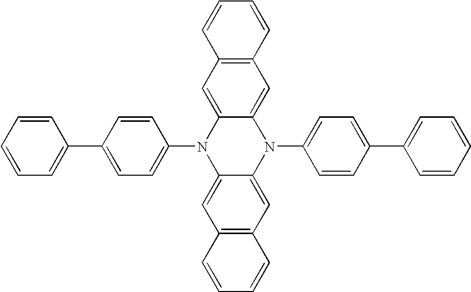 |
(XVI) |
 |
(XVII) |
 |
(XVIII) |
 |
(XIX) |
 |
(XX) |
 |
(XXI) |
 |
(XXII) |
 |
(XXIII) |
 |
(XXIV) |
 |
(XXV) |
 |
(XXVI) |
 |
(XXVII) |
 |
(XXVIII) |
 |
(XXIX) |
 |
(XXX) |
 |
(XXXI) |
 |
(XXXII) |
 |
(XXXIII) |
 |
(XXXIV) |
 |
(XXXV) |
 |
(XXXVI) |
 |
(XXXVII) |
 |
(XXXVIII) |
 |
(XXXIX) |
 |
(XL) |
 |
(XLI) |
 |
(XLII) |
 |
(XLIII) |
 |
(XLIV) |
 |
(XLV) |
 |
(XLVI) |
 |
(XLVII) |
 |
(XLVIII) |
 |
(XLIX) |
 |
(L) |
 |
(LI) |
 |
(LII) |
 |
(LIII) |
 |
(LIV) |
 |
(LV) |
 |
(LVI) |
 |
(LVII) |
 |
(LVIII) |
 |
(LIX) |
 |
(LX) |
 |
(LXI) |
 |
(LXII) |
 |
(LXIII) |
 |
(LXIV) |
 |
(LXV) |
 |
(LXVI) |
 |
(LXVII) |
 |
(LXVIII) |
 |
(LXIX) |
 |
(LXX) |
 |
(LXXI) |
 |
(LXXII) |
 |
(LXXIII) |
 |
(LXXIV) |
 |
(LXXV) |
 |
(LXXVI) |
 |
(LXXVII) |
 |
(LXXVIII) |
 |
(LXXIX) |
 |
(LXXX) |
 |
(LXXXI) |
 |
(LXXXII) |
 |
(LXXXIII) |
 |
(LXXXIV) |
 |
(LXXXV) |
 |
(LXXXVI) |
 |
(LXXXVII) |
 |
(LXXXVIII) |
 |
(LXXXIX) |
 |
(XC) |
 |
(XCI) |
 |
(XCII) |
| ITO: | indium-tin-oxide; used in forming the transparent anode on glass |
| substrates | |
| CFx: | polymerized fluorocarbon layer; used in forming a hole-injecting |
| layer on top of ITO | |
| NPB: | N,N′-di(naphthalene-1-yl)-N,N′-diphenyl-benzidine; used in |
| forming the hole-transporting layer in the organic EL unit, and | |
| also used as the host in forming the p-type doped organic layer | |
| in the connecting unit | |
| Alq: | tris(8-hydroxyquinoline)aluminum(III); used in forming both the |
| electron-transporting layer in the organic EL unit, and also used | |
| as host in forming the n-type doped organic layer in the | |
| connecting unit | |
| F4- | 2,3,5,6-tetrafluoro-7,7′,8,8′-tetracyanoquinodimethane; used as |
| TCNQ: | p-type dopant in forming the p-type doped organic layer in the |
| connecting unit | |
| Li: | Lithium; used as n-type dopant in forming the n-type doped |
| organic layer in the connecting unit | |
| Mg:Ag: | magnesium:silver at a ratio of 10:0.5 by volume; used in forming |
| the cathode. | |
-
- (1) a HTL, 75 nm thick, consisting of NPB;
- (2) an ETL (also serving as the emissive layer), 60 nm thick, consisting of Alq;
- (3) a cathode, approximately 210 nm thick, consisting of Mg:Ag.
-
- (1) a HTL, 90 nm thick, consisting of NPB;
- (2) an ETL (also serving as the emissive layer), 30 nm thick, consisting of Alq; [NPB(90 nm)/Alq(30 nm), denoted as EL1, consists of the 1st EL unit];
- (3) a n-type doped organic layer, 30 nm thick, consisting of Alq host doped with 1.2 vol. % Li;
- (4) a p-type doped organic layer, 60 nm thick, consisting of NPB host doped with 6 vol. % F4-TCNQ [Li doped Alq(30 nm)/F4-TCNQ doped NPB(60 nm) consists of the 1st connecting unit];
- (5) a HTL, 30 nm thick, consisting of NPB;
- (6) a LEL, 30 nm thick, consisting of Alq;
- (7) an
ETL 30 nm thick, consisting of Alq host doped with 1.2 vol. % Li; [NPB(30 nm)/Alq(30 nm)/Alq:Li(30 nm), denoted as EL2, consists of the 2nd EL unit; - (8) a cathode, approximately 210 nm thick, consisting of Mg:Ag.
- 100 cascaded OLED
- 110 anode
- 120 EL unit
- 120.1 1st EL unit
- 120.2 2nd EL unit
- 120. 3rd EL unit
- 120.(N−1) (N−1)th EL unit
- 120.N Nth EL unit
- 130 connecting unit
- 130.1 1st connecting unit
- 130.2 2nd connecting unit
- 130.(N−1) (N−1)th connecting unit
- 131 n-type doped organic layer
- 132 interfacial layer
- 133 p-type doped organic layer
- 140 cathode
- 150 voltage/current source
- 160 electrical conductors
Claims (30)


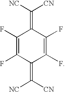


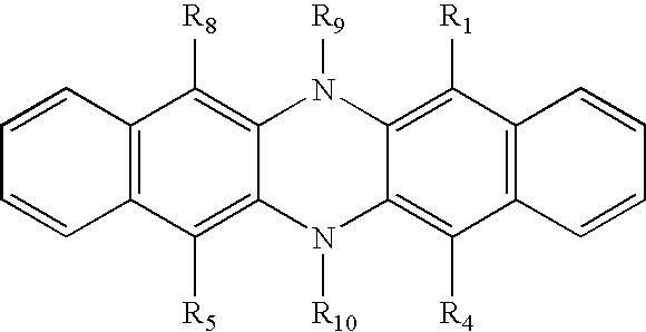


Priority Applications (6)
| Application Number | Priority Date | Filing Date | Title |
|---|---|---|---|
| US10/391,176 US6869699B2 (en) | 2003-03-18 | 2003-03-18 | P-type materials and mixtures for electronic devices |
| TW093102309A TWI348490B (en) | 2003-03-18 | 2004-02-02 | A p-type mixture for use in an electronic device |
| EP04075751A EP1463130A2 (en) | 2003-03-18 | 2004-03-09 | P-type materials and mixtures for electronic devices |
| JP2004076498A JP4813769B2 (en) | 2003-03-18 | 2004-03-17 | P-type material mixture for electronic devices |
| KR1020040017885A KR20040082319A (en) | 2003-03-18 | 2004-03-17 | P-type materials and mixtures for electronic devices |
| CNB2004100287934A CN100483773C (en) | 2003-03-18 | 2004-03-18 | P type material and mikture used for electronic device |
Applications Claiming Priority (1)
| Application Number | Priority Date | Filing Date | Title |
|---|---|---|---|
| US10/391,176 US6869699B2 (en) | 2003-03-18 | 2003-03-18 | P-type materials and mixtures for electronic devices |
Publications (2)
| Publication Number | Publication Date |
|---|---|
| US20040183066A1 US20040183066A1 (en) | 2004-09-23 |
| US6869699B2 true US6869699B2 (en) | 2005-03-22 |
Family
ID=32824854
Family Applications (1)
| Application Number | Title | Priority Date | Filing Date |
|---|---|---|---|
| US10/391,176 Expired - Lifetime US6869699B2 (en) | 2003-03-18 | 2003-03-18 | P-type materials and mixtures for electronic devices |
Country Status (6)
| Country | Link |
|---|---|
| US (1) | US6869699B2 (en) |
| EP (1) | EP1463130A2 (en) |
| JP (1) | JP4813769B2 (en) |
| KR (1) | KR20040082319A (en) |
| CN (1) | CN100483773C (en) |
| TW (1) | TWI348490B (en) |
Cited By (8)
| Publication number | Priority date | Publication date | Assignee | Title |
|---|---|---|---|---|
| US20070238857A1 (en) * | 2006-04-06 | 2007-10-11 | Xerox Corporation | Polydiazaacenes |
| US20070235720A1 (en) * | 2006-04-06 | 2007-10-11 | Xerox Corporation | Polydiazaacenes and electronic devices generated therefrom |
| US20080042556A1 (en) * | 2006-08-18 | 2008-02-21 | Chunghwa Picture Tubes, Ltd | Organic light emitting structure |
| US20090247305A1 (en) * | 2008-03-29 | 2009-10-01 | Hemanth Gundurao Kanekal | Electronic trading card and game system |
| US8330148B2 (en) | 2007-03-02 | 2012-12-11 | Osram Opto Semiconductors Gmbh | Electric organic component and method for the production thereof |
| WO2013172255A1 (en) | 2012-05-17 | 2013-11-21 | 国立大学法人九州大学 | Compound, light emitting material, and organic light emitting element |
| WO2014034535A1 (en) | 2012-08-30 | 2014-03-06 | 国立大学法人九州大学 | Light emitting material, compound and organic light emitting element using light emitting material |
| US9570697B2 (en) | 2003-12-26 | 2017-02-14 | Semiconductor Energy Laboratory Co., Ltd. | Light-emitting element |
Families Citing this family (28)
| Publication number | Priority date | Publication date | Assignee | Title |
|---|---|---|---|---|
| US6991859B2 (en) * | 2003-03-18 | 2006-01-31 | Eastman Kodak Company | Cascaded organic electroluminescent devices |
| US6903378B2 (en) * | 2003-06-26 | 2005-06-07 | Eastman Kodak Company | Stacked OLED display having improved efficiency |
| US7030554B2 (en) * | 2004-02-06 | 2006-04-18 | Eastman Kodak Company | Full-color organic display having improved blue emission |
| JP4461367B2 (en) * | 2004-05-24 | 2010-05-12 | ソニー株式会社 | Display element |
| US7351999B2 (en) * | 2004-12-16 | 2008-04-01 | Au Optronics Corporation | Organic light-emitting device with improved layer structure |
| JP2008530773A (en) * | 2005-02-04 | 2008-08-07 | ノヴァレッド・アクチエンゲゼルシャフト | Additives to organic semiconductors |
| US7494722B2 (en) * | 2005-02-23 | 2009-02-24 | Eastman Kodak Company | Tandem OLED having an organic intermediate connector |
| JP4915544B2 (en) * | 2005-05-11 | 2012-04-11 | パナソニック株式会社 | Organic electroluminescence device |
| US7531959B2 (en) * | 2005-06-29 | 2009-05-12 | Eastman Kodak Company | White light tandem OLED display with filters |
| US7564182B2 (en) * | 2005-06-29 | 2009-07-21 | Eastman Kodak Company | Broadband light tandem OLED display |
| DE102005039608A1 (en) * | 2005-08-19 | 2007-03-01 | Ormecon Gmbh | Composition with intrinsically conductive polymer |
| US7563860B2 (en) * | 2006-04-06 | 2009-07-21 | Xerox Corporation | Semiconductors and electronic devices generated therefrom |
| JP5568305B2 (en) | 2006-09-29 | 2014-08-06 | ユニバーシティ オブ フロリダ リサーチ ファンデーション インコーポレーティッド | Method and apparatus for infrared detection and display |
| SG176831A1 (en) * | 2009-09-07 | 2012-01-30 | Semiconductor Energy Lab | Light-emitting element, light-emitting device, lighting device, and electronic device |
| WO2011052285A1 (en) * | 2009-10-28 | 2011-05-05 | シャープ株式会社 | Novel compound, field-effective transistor, solar cell, method for producing said compound, field-effective transistor, and solar cell, composition for organic semiconductor layer, and composition for p-type semiconductor layer |
| DE102009046859A1 (en) * | 2009-11-19 | 2011-06-30 | Sensient Imaging Technologies GmbH, 06766 | Organic solar cell, useful e.g. in portable electronic applications, comprises a photoactive layer, two electrodes on both sides of the photoactive layer, an electron conducting layer, and a hole transport layer |
| EP2577747B1 (en) | 2010-05-24 | 2018-10-17 | University of Florida Research Foundation, Inc. | Method and apparatus for providing a charge blocking layer on an infrared up-conversion device |
| WO2012067139A1 (en) * | 2010-11-16 | 2012-05-24 | シャープ株式会社 | Compound, field-effect transistor and process for production thereof, solar cell and process for production thereof, organic light-emitting element and process for production thereof, and composition |
| EP2666191A4 (en) | 2011-02-28 | 2018-01-03 | University of Florida Research Foundation, Inc. | Photodetector and upconversion device with gain (ec) |
| BR112013033122A2 (en) * | 2011-06-30 | 2017-01-24 | Nanoholdings Llc | method and apparatus for detecting gain infrared radiation |
| WO2013135352A1 (en) | 2012-03-15 | 2013-09-19 | Merck Patent Gmbh | Electronic devices |
| JP2014082421A (en) | 2012-10-18 | 2014-05-08 | Samsung Display Co Ltd | Organic el material including amine derivative including 5,10-diaryl-5,10-dihydrophenazine moiety, and organic el element using the same |
| KR102135929B1 (en) * | 2013-12-31 | 2020-07-20 | 엘지디스플레이 주식회사 | White Organic Emitting Device |
| CN103985818B (en) * | 2014-04-01 | 2016-04-13 | 上海道亦化工科技有限公司 | A kind of organic electroluminescence device |
| JP6419940B2 (en) * | 2015-03-16 | 2018-11-07 | パイオニア株式会社 | Light emitting device |
| US10749058B2 (en) | 2015-06-11 | 2020-08-18 | University Of Florida Research Foundation, Incorporated | Monodisperse, IR-absorbing nanoparticles and related methods and devices |
| CN112079786A (en) * | 2019-06-14 | 2020-12-15 | 北京鼎材科技有限公司 | Compound, organic electronic light-emitting device comprising compound and application of compound |
| CN111072578A (en) * | 2019-11-25 | 2020-04-28 | 武汉华星光电半导体显示技术有限公司 | P-type dopant and organic light emitting diode |
Citations (13)
| Publication number | Priority date | Publication date | Assignee | Title |
|---|---|---|---|---|
| US3172862A (en) | 1960-09-29 | 1965-03-09 | Dow Chemical Co | Organic electroluminescent phosphors |
| US3173050A (en) | 1962-09-19 | 1965-03-09 | Dow Chemical Co | Electroluminescent cell |
| US3710167A (en) | 1970-07-02 | 1973-01-09 | Rca Corp | Organic electroluminescent cells having a tunnel injection cathode |
| US4356429A (en) | 1980-07-17 | 1982-10-26 | Eastman Kodak Company | Organic electroluminescent cell |
| US4505841A (en) | 1982-11-17 | 1985-03-19 | Chevron Research Company | Fused 6,6,6-membered heterocyclic electroactive polymers |
| US4769292A (en) | 1987-03-02 | 1988-09-06 | Eastman Kodak Company | Electroluminescent device with modified thin film luminescent zone |
| US5703436A (en) | 1994-12-13 | 1997-12-30 | The Trustees Of Princeton University | Transparent contacts for organic devices |
| JP2000021574A (en) | 1998-06-29 | 2000-01-21 | Canon Inc | Light emitting element |
| JP2000260565A (en) * | 1999-03-04 | 2000-09-22 | Futaba Corp | Organic el element |
| US6274980B1 (en) | 1998-11-16 | 2001-08-14 | The Trustees Of Princeton University | Single-color stacked organic light emitting device |
| US6337492B1 (en) | 1997-07-11 | 2002-01-08 | Emagin Corporation | Serially-connected organic light emitting diode stack having conductors sandwiching each light emitting layer |
| US6486601B1 (en) * | 1998-06-26 | 2002-11-26 | Idemitsu Kosan Co., Ltd. | Organic luminescence device with reduced leakage current |
| US20040004433A1 (en) * | 2002-06-26 | 2004-01-08 | 3M Innovative Properties Company | Buffer layers for organic electroluminescent devices and methods of manufacture and use |
Family Cites Families (4)
| Publication number | Priority date | Publication date | Assignee | Title |
|---|---|---|---|---|
| JPS6073562A (en) * | 1983-09-02 | 1985-04-25 | ボルウエル デイベロプメンツ プロプライアタリー リミテイド | Simulator apparatus |
| JP3150750B2 (en) * | 1992-03-13 | 2001-03-26 | 日本写真印刷株式会社 | Organic rectifier |
| JP3580078B2 (en) * | 1997-04-07 | 2004-10-20 | 東洋インキ製造株式会社 | Organic electroluminescent device material and organic electroluminescent device using the same |
| JP3503403B2 (en) * | 1997-03-17 | 2004-03-08 | 東洋インキ製造株式会社 | Light emitting material for organic electroluminescent device and organic electroluminescent device using the same |
-
2003
- 2003-03-18 US US10/391,176 patent/US6869699B2/en not_active Expired - Lifetime
-
2004
- 2004-02-02 TW TW093102309A patent/TWI348490B/en not_active IP Right Cessation
- 2004-03-09 EP EP04075751A patent/EP1463130A2/en not_active Withdrawn
- 2004-03-17 KR KR1020040017885A patent/KR20040082319A/en not_active Application Discontinuation
- 2004-03-17 JP JP2004076498A patent/JP4813769B2/en not_active Expired - Lifetime
- 2004-03-18 CN CNB2004100287934A patent/CN100483773C/en not_active Expired - Lifetime
Patent Citations (13)
| Publication number | Priority date | Publication date | Assignee | Title |
|---|---|---|---|---|
| US3172862A (en) | 1960-09-29 | 1965-03-09 | Dow Chemical Co | Organic electroluminescent phosphors |
| US3173050A (en) | 1962-09-19 | 1965-03-09 | Dow Chemical Co | Electroluminescent cell |
| US3710167A (en) | 1970-07-02 | 1973-01-09 | Rca Corp | Organic electroluminescent cells having a tunnel injection cathode |
| US4356429A (en) | 1980-07-17 | 1982-10-26 | Eastman Kodak Company | Organic electroluminescent cell |
| US4505841A (en) | 1982-11-17 | 1985-03-19 | Chevron Research Company | Fused 6,6,6-membered heterocyclic electroactive polymers |
| US4769292A (en) | 1987-03-02 | 1988-09-06 | Eastman Kodak Company | Electroluminescent device with modified thin film luminescent zone |
| US5703436A (en) | 1994-12-13 | 1997-12-30 | The Trustees Of Princeton University | Transparent contacts for organic devices |
| US6337492B1 (en) | 1997-07-11 | 2002-01-08 | Emagin Corporation | Serially-connected organic light emitting diode stack having conductors sandwiching each light emitting layer |
| US6486601B1 (en) * | 1998-06-26 | 2002-11-26 | Idemitsu Kosan Co., Ltd. | Organic luminescence device with reduced leakage current |
| JP2000021574A (en) | 1998-06-29 | 2000-01-21 | Canon Inc | Light emitting element |
| US6274980B1 (en) | 1998-11-16 | 2001-08-14 | The Trustees Of Princeton University | Single-color stacked organic light emitting device |
| JP2000260565A (en) * | 1999-03-04 | 2000-09-22 | Futaba Corp | Organic el element |
| US20040004433A1 (en) * | 2002-06-26 | 2004-01-08 | 3M Innovative Properties Company | Buffer layers for organic electroluminescent devices and methods of manufacture and use |
Non-Patent Citations (4)
| Title |
|---|
| "Double Injection Electroluminescence in Anthracene" by J. Dresner, RCA Review, 30, 322-334 (1969). |
| "Electroluminescence of doped organic thin films" by C. W. Tang et al., J. Appl. Physics 65 (9), May 1, 1989, pp. 3610-3616. |
| Bruhlmann et al., The Journal of Physical Chemistry, vol. 81, No. 5, (1977), p. 386-391.* * |
| U.S. Appl. No. 10/145,363, filed May 14, 2002, Parton et al. |
Cited By (14)
| Publication number | Priority date | Publication date | Assignee | Title |
|---|---|---|---|---|
| US9570697B2 (en) | 2003-12-26 | 2017-02-14 | Semiconductor Energy Laboratory Co., Ltd. | Light-emitting element |
| US10886497B2 (en) | 2003-12-26 | 2021-01-05 | Semiconductor Energy Laboratory Co., Ltd. | Light-emitting element |
| US20070235720A1 (en) * | 2006-04-06 | 2007-10-11 | Xerox Corporation | Polydiazaacenes and electronic devices generated therefrom |
| US7517477B2 (en) * | 2006-04-06 | 2009-04-14 | Xerox Corporation | Polydiazaacenes and electronic devices generated therefrom |
| US7517476B2 (en) * | 2006-04-06 | 2009-04-14 | Xerox Corporation | Polydiazaacenes |
| US20070238857A1 (en) * | 2006-04-06 | 2007-10-11 | Xerox Corporation | Polydiazaacenes |
| US20080042556A1 (en) * | 2006-08-18 | 2008-02-21 | Chunghwa Picture Tubes, Ltd | Organic light emitting structure |
| US8330148B2 (en) | 2007-03-02 | 2012-12-11 | Osram Opto Semiconductors Gmbh | Electric organic component and method for the production thereof |
| US8608573B2 (en) | 2008-03-29 | 2013-12-17 | Hemanth Gundurao Kanekal | Electronic trading card and game system |
| US9393484B2 (en) | 2008-03-29 | 2016-07-19 | Hemanth Gundurao Kanekal | Electronic trading card and game system |
| US20090247305A1 (en) * | 2008-03-29 | 2009-10-01 | Hemanth Gundurao Kanekal | Electronic trading card and game system |
| WO2013172255A1 (en) | 2012-05-17 | 2013-11-21 | 国立大学法人九州大学 | Compound, light emitting material, and organic light emitting element |
| US9660199B2 (en) | 2012-05-17 | 2017-05-23 | Kyulux, Inc. | Compound, light-emitting material, and organic light-emitting device |
| WO2014034535A1 (en) | 2012-08-30 | 2014-03-06 | 国立大学法人九州大学 | Light emitting material, compound and organic light emitting element using light emitting material |
Also Published As
| Publication number | Publication date |
|---|---|
| EP1463130A2 (en) | 2004-09-29 |
| CN100483773C (en) | 2009-04-29 |
| KR20040082319A (en) | 2004-09-24 |
| TW200500441A (en) | 2005-01-01 |
| JP2004281408A (en) | 2004-10-07 |
| JP4813769B2 (en) | 2011-11-09 |
| US20040183066A1 (en) | 2004-09-23 |
| CN1532959A (en) | 2004-09-29 |
| TWI348490B (en) | 2011-09-11 |
Similar Documents
| Publication | Publication Date | Title |
|---|---|---|
| US6869699B2 (en) | P-type materials and mixtures for electronic devices | |
| US6991859B2 (en) | Cascaded organic electroluminescent devices | |
| US6717358B1 (en) | Cascaded organic electroluminescent devices with improved voltage stability | |
| US6936961B2 (en) | Cascaded organic electroluminescent device having connecting units with N-type and P-type organic layers | |
| US8237157B2 (en) | Fluorocarbon electrode modification layer | |
| US6881502B2 (en) | Blue organic electroluminescent devices having a non-hole-blocking layer | |
| US7494722B2 (en) | Tandem OLED having an organic intermediate connector | |
| US6875320B2 (en) | Highly transparent top electrode for OLED device | |
| US8057916B2 (en) | OLED device with improved performance | |
| US7126267B2 (en) | Tandem OLED having stable intermediate connectors | |
| US6872472B2 (en) | Providing an organic electroluminescent device having stacked electroluminescent units | |
| EP1704604B1 (en) | Using a crystallization-inhibitor in organic electroluminescent devices | |
| EP1668717B1 (en) | Metal sub-layer within a hole-transporting region | |
| US7075231B1 (en) | Tandem OLEDs having low drive voltage | |
| US20060240277A1 (en) | Tandem OLED device | |
| US20090191428A1 (en) | Tandem oled device with intermediate connector | |
| US6919140B2 (en) | Organic electroluminescent devices with high luminance |
Legal Events
| Date | Code | Title | Description |
|---|---|---|---|
| AS | Assignment |
Owner name: EASTMAN KODAK COMPANY, NEW YORK Free format text: ASSIGNMENT OF ASSIGNORS INTEREST;ASSIGNORS:KLUBEK, KEVIN P.;LIAO, LIANG-SHENG;VARGAS, J. R.;AND OTHERS;REEL/FRAME:013889/0718;SIGNING DATES FROM 20030313 TO 20030317 |
|
| FEPP | Fee payment procedure |
Free format text: PAYOR NUMBER ASSIGNED (ORIGINAL EVENT CODE: ASPN); ENTITY STATUS OF PATENT OWNER: LARGE ENTITY |
|
| STCF | Information on status: patent grant |
Free format text: PATENTED CASE |
|
| FPAY | Fee payment |
Year of fee payment: 4 |
|
| FEPP | Fee payment procedure |
Free format text: PAYER NUMBER DE-ASSIGNED (ORIGINAL EVENT CODE: RMPN); ENTITY STATUS OF PATENT OWNER: LARGE ENTITY Free format text: PAYOR NUMBER ASSIGNED (ORIGINAL EVENT CODE: ASPN); ENTITY STATUS OF PATENT OWNER: LARGE ENTITY |
|
| AS | Assignment |
Owner name: GLOBAL OLED TECHNOLOGY LLC,DELAWARE Free format text: ASSIGNMENT OF ASSIGNORS INTEREST;ASSIGNOR:EASTMAN KODAK COMPANY;REEL/FRAME:023998/0368 Effective date: 20100122 Owner name: GLOBAL OLED TECHNOLOGY LLC, DELAWARE Free format text: ASSIGNMENT OF ASSIGNORS INTEREST;ASSIGNOR:EASTMAN KODAK COMPANY;REEL/FRAME:023998/0368 Effective date: 20100122 |
|
| FPAY | Fee payment |
Year of fee payment: 8 |
|
| FPAY | Fee payment |
Year of fee payment: 12 |