US6830649B2 - Apparatus and method for producing semiconductors - Google Patents
Apparatus and method for producing semiconductors Download PDFInfo
- Publication number
- US6830649B2 US6830649B2 US10/080,539 US8053902A US6830649B2 US 6830649 B2 US6830649 B2 US 6830649B2 US 8053902 A US8053902 A US 8053902A US 6830649 B2 US6830649 B2 US 6830649B2
- Authority
- US
- United States
- Prior art keywords
- wafer
- unit
- etching
- measuring instrument
- wetting
- Prior art date
- Legal status (The legal status is an assumption and is not a legal conclusion. Google has not performed a legal analysis and makes no representation as to the accuracy of the status listed.)
- Expired - Fee Related
Links
Images


Classifications
-
- H—ELECTRICITY
- H10—SEMICONDUCTOR DEVICES; ELECTRIC SOLID-STATE DEVICES NOT OTHERWISE PROVIDED FOR
- H10P—GENERIC PROCESSES OR APPARATUS FOR THE MANUFACTURE OR TREATMENT OF DEVICES COVERED BY CLASS H10
- H10P50/00—Etching of wafers, substrates or parts of devices
-
- H—ELECTRICITY
- H10—SEMICONDUCTOR DEVICES; ELECTRIC SOLID-STATE DEVICES NOT OTHERWISE PROVIDED FOR
- H10P—GENERIC PROCESSES OR APPARATUS FOR THE MANUFACTURE OR TREATMENT OF DEVICES COVERED BY CLASS H10
- H10P72/00—Handling or holding of wafers, substrates or devices during manufacture or treatment thereof
- H10P72/04—Apparatus for manufacture or treatment
- H10P72/0451—Apparatus for manufacturing or treating in a plurality of work-stations
- H10P72/0452—Apparatus for manufacturing or treating in a plurality of work-stations characterised by the layout of the process chambers
- H10P72/0454—Apparatus for manufacturing or treating in a plurality of work-stations characterised by the layout of the process chambers surrounding a central transfer chamber
-
- H—ELECTRICITY
- H10—SEMICONDUCTOR DEVICES; ELECTRIC SOLID-STATE DEVICES NOT OTHERWISE PROVIDED FOR
- H10P—GENERIC PROCESSES OR APPARATUS FOR THE MANUFACTURE OR TREATMENT OF DEVICES COVERED BY CLASS H10
- H10P72/00—Handling or holding of wafers, substrates or devices during manufacture or treatment thereof
- H10P72/04—Apparatus for manufacture or treatment
- H10P72/0451—Apparatus for manufacturing or treating in a plurality of work-stations
- H10P72/0468—Apparatus for manufacturing or treating in a plurality of work-stations comprising a chamber adapted to a particular process
-
- H—ELECTRICITY
- H10—SEMICONDUCTOR DEVICES; ELECTRIC SOLID-STATE DEVICES NOT OTHERWISE PROVIDED FOR
- H10P—GENERIC PROCESSES OR APPARATUS FOR THE MANUFACTURE OR TREATMENT OF DEVICES COVERED BY CLASS H10
- H10P72/00—Handling or holding of wafers, substrates or devices during manufacture or treatment thereof
- H10P72/30—Handling or holding of wafers, substrates or devices during manufacture or treatment thereof for conveying, e.g. between different workstations
- H10P72/33—Handling or holding of wafers, substrates or devices during manufacture or treatment thereof for conveying, e.g. between different workstations into and out of processing chamber
- H10P72/3304—Handling or holding of wafers, substrates or devices during manufacture or treatment thereof for conveying, e.g. between different workstations into and out of processing chamber characterised by movements or sequence of movements of transfer devices
-
- H—ELECTRICITY
- H10—SEMICONDUCTOR DEVICES; ELECTRIC SOLID-STATE DEVICES NOT OTHERWISE PROVIDED FOR
- H10P—GENERIC PROCESSES OR APPARATUS FOR THE MANUFACTURE OR TREATMENT OF DEVICES COVERED BY CLASS H10
- H10P50/00—Etching of wafers, substrates or parts of devices
- H10P50/20—Dry etching; Plasma etching; Reactive-ion etching
- H10P50/28—Dry etching; Plasma etching; Reactive-ion etching of insulating materials
- H10P50/286—Dry etching; Plasma etching; Reactive-ion etching of insulating materials of organic materials
- H10P50/287—Dry etching; Plasma etching; Reactive-ion etching of insulating materials of organic materials by chemical means
-
- H—ELECTRICITY
- H10—SEMICONDUCTOR DEVICES; ELECTRIC SOLID-STATE DEVICES NOT OTHERWISE PROVIDED FOR
- H10P—GENERIC PROCESSES OR APPARATUS FOR THE MANUFACTURE OR TREATMENT OF DEVICES COVERED BY CLASS H10
- H10P70/00—Cleaning of wafers, substrates or parts of devices
- H10P70/20—Cleaning during device manufacture
- H10P70/27—Cleaning during device manufacture during, before or after processing of conductive materials, e.g. polysilicon or amorphous silicon layers
- H10P70/273—Cleaning during device manufacture during, before or after processing of conductive materials, e.g. polysilicon or amorphous silicon layers the processing being a delineation of conductive layers, e.g. by RIE
-
- H—ELECTRICITY
- H10—SEMICONDUCTOR DEVICES; ELECTRIC SOLID-STATE DEVICES NOT OTHERWISE PROVIDED FOR
- H10P—GENERIC PROCESSES OR APPARATUS FOR THE MANUFACTURE OR TREATMENT OF DEVICES COVERED BY CLASS H10
- H10P74/00—Testing or measuring during manufacture or treatment of wafers, substrates or devices
- H10P74/20—Testing or measuring during manufacture or treatment of wafers, substrates or devices characterised by the properties tested or measured, e.g. structural or electrical properties
- H10P74/203—Structural properties, e.g. testing or measuring thicknesses, line widths, warpage, bond strengths or physical defects
-
- Y—GENERAL TAGGING OF NEW TECHNOLOGICAL DEVELOPMENTS; GENERAL TAGGING OF CROSS-SECTIONAL TECHNOLOGIES SPANNING OVER SEVERAL SECTIONS OF THE IPC; TECHNICAL SUBJECTS COVERED BY FORMER USPC CROSS-REFERENCE ART COLLECTIONS [XRACs] AND DIGESTS
- Y10—TECHNICAL SUBJECTS COVERED BY FORMER USPC
- Y10S—TECHNICAL SUBJECTS COVERED BY FORMER USPC CROSS-REFERENCE ART COLLECTIONS [XRACs] AND DIGESTS
- Y10S414/00—Material or article handling
- Y10S414/135—Associated with semiconductor wafer handling
- Y10S414/139—Associated with semiconductor wafer handling including wafer charging or discharging means for vacuum chamber
Definitions
- the present invention relates to an apparatus and a method for producing semiconductors, particularly to a semiconductor producing apparatus and method which are suited for conducting desired etching on semiconductor wafers.
- FIG. 6 is a schematic illustration of a typical conventional etching system.
- reference numeral 1 indicates an etching unit which etches the wafer (semiconductor wafer) by making use of plasma generated under reduced pressure.
- the wafer is worked in conformity to the mask pattern formed on said wafer.
- Numeral 2 designates an ashing unit which removes the mask remaining on the wafer immediately after etching by ashing process.
- Numeral 3 is a wafer transport means whereby the wafers contained in a cassette 5 are transported to said units.
- Numeral 4 refers to a wafer, such as a semiconductor wafer, which is to be etched
- numeral 5 denotes a wafer cassette, which is a jig for transporting the wafers such as semiconductor wafers to be etched. Approximately 25 sheets of wafer are contained in each cassette which is properly set in the etching system 6 .
- FIG. 7 is a diagram (flow chart and time chart) showing a process of treatments of a wafer (semiconductor wafer) by the said conventional etching system 6 .
- the wafer On completing the etching work by the etching unit 1 , the wafer is carried to the ashing unit 2 one by one by the transport means 3 and ashed by said unit 2 .
- the wafer which has finished the ashing treatment is then placed in the cassette 5 .
- the wafer-loaded cassette 5 is taken out and transported to a wetting unit not shown.
- the wafer is subjected to a wetting treatment (e.g., for peeling of the side wall) by the wetting unit.
- the wafer-containing cassette is transferred to a measuring device not shown, and in step 7 , the post-treatment measurement of size is made.
- each working unit is basically designed to perform treatment on the lot base, that is, according to this system, only after the whole number (lot) of the wafers contained in a cassette have been finished with one treatment, they are allowed to proceed to the next treatment step.
- the treatment by each working unit is conducted on the lot base as shown by the time chart of FIG. 7 . Therefore, according to this system, even if a failure or fault should be detected in step 7 (step for post-treatment measurements) which is the final step, the etching treatment for that lot is already finished, and there is a possibility that many non-conforming wafers exist in the lot.
- the semiconductor producing apparatus comprises an integrated measuring instrument for measuring the form or size of the element to be formed into a wafer, an etching unit for etching said wafer by making use of plasma generated under reduced pressure, an ashing unit for ashing said etched wafer, a wetting unit for wetting the etched wafer, a drying unit for drying the wafer which has finished said wetting treatment, a transport means by which said wafers taken into a wafer cassette are transported successively one by one to said integrated measuring instrument and said treating units, and a transport chamber in which said integrated measuring instrument, etching unit; ashing unit, wetting unit, drying unit and transport means are connected to a transport passage designed to be capable of being reduced in pressure, and which is provided with a wafer cassette inlet for receiving the cassette containing a plural number of sheets of wafer to be etched.
- FIG. 1 is a drawing illustrating the side wall protective film formed by etching.
- FIG. 2 is a drawing illustrating the process of measurement by the integrated measuring instrument.
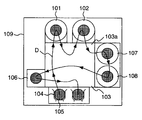
- FIG. 3 is a schematic illustration of the semiconductor producing apparatus in an embodiment of the present invention.
- FIG. 4 is a drawing illustrating the integrating process by the semiconductor producing apparatus.
- FIG. 5 is a drawing illustrating the treatments for each wafer by the semiconductor producing apparatus.
- FIG. 6 is a schematic illustration of a typical conventional etching system.
- FIG. 7 is a drawing illustrating the treatments for each wafer (semiconductor wafer).
- Control of characteristics (operating point) of transistors in the element manufacturing process is usually effected by controlling the gate length (CD value) of transistors.
- CD value the gate length of transistors.
- the scatter of CD value allowed in the gate etching process is approximately 5 nm.
- etching operation is carried out by supplying an additive gas (for example, O 2 or CF type gas) to the reactive gas (for example, Cl 2 or HBr).
- the additive gas serves for forming a film (for example, a material containing Si and O or a material containing Si and C) on the side of the element during working to produce an effect as a side wall protective film for preventing further advance of working on the side of the element.
- the side wall protective film may thicken to about 1 to 5 nm, so that such a film needs to be removed after etching.
- the formed protective film is small in thickness, there is a possibility that the element such as Cl or Br used for etching would remain in the protective film, so that it is necessary to remove the protective film by a cleansing step.
- FIG. 1 illustrates the side wall protective film formed by etching, wherein FIG. 1 ( a ) shows the condition of the wafer (wafer) before etching and FIG. 1 ( b ) shows the condition after etching.
- reference numeral 11 indicates a silicon substrate, 12 a ground film, 13 a material to be etched, and 14 a resist pattern.
- Numeral 15 in the drawing refers to the side wall protective film formed on the side of said material by etching.
- the thickness (1-5 nm) of the side wall protective film is an amount unnegligible in view of the controlled value of CD. Therefore, in control of the CD value in the semiconductor element manufacturing process, the presence of the protective film can not be ignored.
- FIG. 2 is a diagrammatic chart illustrating the measuring process by an integrated measuring instrument.
- OCD optical Critical Dimension measuring instrument
- said characteristics library is prepared by making use of simulation techniques.
- the expected form of the subject of measurement, film structure and optical constants such as refractive index (n) and extinction coefficient (k) are input. Therefore, in case said input information of the wafer to be measured is unavailable, it is impossible to make measurements of the subject wafer.
- an atomic force microscope which makes use of interatomic force of material can be used.
- This device requires much time for the measurement, so that it is unpractical as a meter which is expected to make measurement in the course of the treating process as in the present invention.
- FIG. 3 is a schematic illustration of the semiconductor manufacturing system in an embodiment of the present invention.
- numeral 101 designates an etching unit which etches the wafer (semiconductor wafer) by making use of plasma generated under reduced pressure.
- the wafer is worked in conformity to the mask pattern formed on said wafer.
- Numeral 102 refers to an ashing unit which ashes away the mask remaining on the wafer immediately after etching.
- 103 indicates a wafer transport means comprising a transport passage 103 a which can be depressurized.
- This transport means is capable of transporting the wafers contained in a cassette to the integrated measuring instrument and other working units, without being exposed to the air, along said depressurizable transport passage 103 a.
- 107 is a wetting unit which functions to remove the corrosive substances produced by the etching work to prevent corrosion of the etched wafer.
- a side wall protective film may deposit on the wall surface of the etched material as mentioned before. It is a role of said wetting unit to remove this side wall film.
- 108 is a drying unit which dries the wafer which has gone through the wetting treatment.
- This integrated measuring instrument 106 denotes an integrated measuring instrument which measures the fine worked form of the wafer before and after the treatment done by said etching unit 101 . As measurement of the wafer is made after the treatment by said wetting unit 107 , it is possible to make correct measurement of form and film thickness, free from the influence of said side wall protective film.
- This integrated measuring instrument 106 can be operated either under normal pressure or under reduced pressure, so that it may be mounted at a position in the wafer alignment mechanism set under normal pressure or the load lock chamber under reduced pressure, or halfway on the atmospheric air transport passage or wafer transport route, or alongside with any of said working units. As for the way of mounting of this metrology 106 , it may be directly installed at any of the above-said positions, or may be fitted in the upper part of a quartz window disposed at any of said positions.
- 104 represents the wafers such as semiconductor wafers which are to be etched, and 105 designates a fixture which aids transport of the wafer such as semiconductor wafer to be etched. Approximately 25 sheets of wafer are contained in each cassette which is set in position in the etching system 6 .
- a load lock chamber may be provided between said integrated measuring instrument 106 , each treating unit and said depressurizable transport passage 103 a .
- the transport passage between said wetting unit 107 and drying unit 108 is preferably designed to connect them directly without interposition of said depressurizable transport passage.
- Traffic line D in the drawing shows the wafer transport route, representing an example of the process in which the wafer is treated.
- the wafer which has completed the work by the integral treating system 109 is put back in the cassette 104 and carried to the next step through an inlet port not shown.
- FIG. 4 is a schematic chart illustrating the integral process (through-process) by said semiconductor manufacturing system 109 .
- this semiconductor manufacturing system comprises an integral metrology, an etching unit, an ashing unit, a wetting unit, a drying unit and a wafer transport means.
- the wafer transport means By the wafer transport means, the wafers (wafers) contained in each wafer cassette are transported one by one successively to the integrated measuring instrument and each working unit.
- the form or size of each received wafer is measured in step 21 .
- the wafer is etched in step 22 .
- it is possible to rectify the scatter of work in the preceding step by controlling the etching conditions (feed forward controlling) based on the form or the measured values of geometry.
- the wafer may be immediately subjected to etching work in step 22 by skipping step 21 .
- the etching conditions may be controlled (feed forward controlling) based on the results of measurements in the inspection step before the said preceding step.
- FIG. 5 is the diagrams (flow chart and time chart) illustrating the treating process of each wafer (semiconductor wafer) by the semiconductor manufacturing system.
- this semiconductor manufacturing system is provided with a wafer transport means whereby the wafers contained in the cassette 5 are transported one by one to the integrated measuring instrument and each working unit, without being exposed to the outer air, along said depressurizable transport passage 103 a.
- the cassette 105 containing the wafers which have got through the preceding steps is set in the semiconductor manufacturing system 109 .
- pre-treatment measurements (measurement of size, etc.) of the wafer are made.
- the wafers contained in the cassette are carried one by one continuously to the integrated measuring instrument 106 and measured successively.
- the wafers which have finished the measurements are conveyed one by one continuously to the etching unit 101 and etched one by one.
- the etched wafers are then led one by one continuously to the ashing unit 102 and ashed one by one.
- the ashed wafers are transported one by one continuously to the wetting unit 108 to go through the wetting treatment.
- step 34 the wafers which have gone through the-wetting treatment are subjected to drying operation and then carried one by one continuously to the integrated measuring instrument 106 whereby the form or size of each wafer is measured. The above process is repeated until one whole lot of the wafers are finished with all said treatments (step 35 ).
Landscapes
- Drying Of Semiconductors (AREA)
- Testing Or Measuring Of Semiconductors Or The Like (AREA)
Abstract
Description
Claims (25)
Applications Claiming Priority (2)
| Application Number | Priority Date | Filing Date | Title |
|---|---|---|---|
| JP2001384872A JP3686866B2 (en) | 2001-12-18 | 2001-12-18 | Semiconductor manufacturing apparatus and manufacturing method |
| JP2001-384872 | 2001-12-18 |
Publications (2)
| Publication Number | Publication Date |
|---|---|
| US20030114011A1 US20030114011A1 (en) | 2003-06-19 |
| US6830649B2 true US6830649B2 (en) | 2004-12-14 |
Family
ID=19187766
Family Applications (1)
| Application Number | Title | Priority Date | Filing Date |
|---|---|---|---|
| US10/080,539 Expired - Fee Related US6830649B2 (en) | 2001-12-18 | 2002-02-25 | Apparatus and method for producing semiconductors |
Country Status (4)
| Country | Link |
|---|---|
| US (1) | US6830649B2 (en) |
| JP (1) | JP3686866B2 (en) |
| KR (1) | KR100877361B1 (en) |
| TW (1) | TW536750B (en) |
Cited By (2)
| Publication number | Priority date | Publication date | Assignee | Title |
|---|---|---|---|---|
| US20040260420A1 (en) * | 2003-06-20 | 2004-12-23 | Tokyo Electron Limited. | Processing method and processing system |
| US20050218337A1 (en) * | 2004-03-30 | 2005-10-06 | Yoshitaka Kai | Vacuum processing apparatus and vacuum processing method |
Families Citing this family (2)
| Publication number | Priority date | Publication date | Assignee | Title |
|---|---|---|---|---|
| CN100388451C (en) * | 2004-11-02 | 2008-05-14 | 力晶半导体股份有限公司 | Defect detection method |
| KR102496037B1 (en) * | 2016-01-20 | 2023-02-06 | 삼성전자주식회사 | method and apparatus for plasma etching |
Citations (17)
| Publication number | Priority date | Publication date | Assignee | Title |
|---|---|---|---|---|
| US5135608A (en) * | 1989-07-11 | 1992-08-04 | Hitachi, Ltd. | Method of producing semiconductor devices |
| US5310410A (en) * | 1990-04-06 | 1994-05-10 | Sputtered Films, Inc. | Method for processing semi-conductor wafers in a multiple vacuum and non-vacuum chamber apparatus |
| JPH06302557A (en) * | 1993-04-15 | 1994-10-28 | Nec Yamaguchi Ltd | Dry-etching apparatus |
| US5474641A (en) * | 1992-10-23 | 1995-12-12 | Tokyo Electron Kabushiki Kaisha | Processing method and apparatus thereof |
| US5695564A (en) * | 1994-08-19 | 1997-12-09 | Tokyo Electron Limited | Semiconductor processing system |
| US5766360A (en) * | 1992-03-27 | 1998-06-16 | Kabushiki Kaisha Toshiba | Substrate processing apparatus and substrate processing method |
| US5769952A (en) * | 1994-06-07 | 1998-06-23 | Tokyo Electron, Ltd. | Reduced pressure and normal pressure treatment apparatus |
| US5913978A (en) * | 1995-04-20 | 1999-06-22 | Tokyo Electron Ltd. | Apparatus and method for regulating pressure in two chambers |
| US5934856A (en) * | 1994-05-23 | 1999-08-10 | Tokyo Electron Limited | Multi-chamber treatment system |
| US5940175A (en) * | 1996-11-01 | 1999-08-17 | Msp Corporation | Method and apparatus for surface inspection in a chamber |
| US5963329A (en) * | 1997-10-31 | 1999-10-05 | International Business Machines Corporation | Method and apparatus for measuring the profile of small repeating lines |
| US6042623A (en) * | 1998-01-12 | 2000-03-28 | Tokyo Electron Limited | Two-wafer loadlock wafer processing apparatus and loading and unloading method therefor |
| JP2000173530A (en) * | 1998-12-04 | 2000-06-23 | Nec Corp | Ion implantation device and ion implantation detecting method |
| US6106659A (en) * | 1997-07-14 | 2000-08-22 | The University Of Tennessee Research Corporation | Treater systems and methods for generating moderate-to-high-pressure plasma discharges for treating materials and related treated materials |
| US6264748B1 (en) * | 1997-08-15 | 2001-07-24 | Tokyo Electron Limited | Substrate processing apparatus |
| US20020155629A1 (en) * | 2000-11-20 | 2002-10-24 | Fairbairn Kevin P. | Semiconductor processing module with integrated feedback/feed forward metrology |
| US20030082466A1 (en) * | 2001-10-19 | 2003-05-01 | Asml, Lithography Division | Wafer handling system and method for use in lithography patterning |
Family Cites Families (5)
| Publication number | Priority date | Publication date | Assignee | Title |
|---|---|---|---|---|
| JPS5617022A (en) * | 1979-07-20 | 1981-02-18 | Hitachi Ltd | Treating apparatus |
| JPH04107821A (en) * | 1990-08-28 | 1992-04-09 | Nec Corp | Dry etching system |
| JP2764027B2 (en) * | 1996-01-29 | 1998-06-11 | 株式会社日立製作所 | Sample processing method and apparatus |
| KR100561703B1 (en) * | 1998-11-12 | 2006-03-17 | 동경 엘렉트론 주식회사 | Processing system |
| US6413867B1 (en) * | 1999-12-23 | 2002-07-02 | Applied Materials, Inc. | Film thickness control using spectral interferometry |
-
2001
- 2001-12-18 JP JP2001384872A patent/JP3686866B2/en not_active Expired - Fee Related
-
2002
- 2002-02-25 US US10/080,539 patent/US6830649B2/en not_active Expired - Fee Related
- 2002-03-07 TW TW091104311A patent/TW536750B/en not_active IP Right Cessation
- 2002-03-11 KR KR1020020012839A patent/KR100877361B1/en not_active Expired - Fee Related
Patent Citations (17)
| Publication number | Priority date | Publication date | Assignee | Title |
|---|---|---|---|---|
| US5135608A (en) * | 1989-07-11 | 1992-08-04 | Hitachi, Ltd. | Method of producing semiconductor devices |
| US5310410A (en) * | 1990-04-06 | 1994-05-10 | Sputtered Films, Inc. | Method for processing semi-conductor wafers in a multiple vacuum and non-vacuum chamber apparatus |
| US5766360A (en) * | 1992-03-27 | 1998-06-16 | Kabushiki Kaisha Toshiba | Substrate processing apparatus and substrate processing method |
| US5474641A (en) * | 1992-10-23 | 1995-12-12 | Tokyo Electron Kabushiki Kaisha | Processing method and apparatus thereof |
| JPH06302557A (en) * | 1993-04-15 | 1994-10-28 | Nec Yamaguchi Ltd | Dry-etching apparatus |
| US5934856A (en) * | 1994-05-23 | 1999-08-10 | Tokyo Electron Limited | Multi-chamber treatment system |
| US5769952A (en) * | 1994-06-07 | 1998-06-23 | Tokyo Electron, Ltd. | Reduced pressure and normal pressure treatment apparatus |
| US5695564A (en) * | 1994-08-19 | 1997-12-09 | Tokyo Electron Limited | Semiconductor processing system |
| US5913978A (en) * | 1995-04-20 | 1999-06-22 | Tokyo Electron Ltd. | Apparatus and method for regulating pressure in two chambers |
| US5940175A (en) * | 1996-11-01 | 1999-08-17 | Msp Corporation | Method and apparatus for surface inspection in a chamber |
| US6106659A (en) * | 1997-07-14 | 2000-08-22 | The University Of Tennessee Research Corporation | Treater systems and methods for generating moderate-to-high-pressure plasma discharges for treating materials and related treated materials |
| US6264748B1 (en) * | 1997-08-15 | 2001-07-24 | Tokyo Electron Limited | Substrate processing apparatus |
| US5963329A (en) * | 1997-10-31 | 1999-10-05 | International Business Machines Corporation | Method and apparatus for measuring the profile of small repeating lines |
| US6042623A (en) * | 1998-01-12 | 2000-03-28 | Tokyo Electron Limited | Two-wafer loadlock wafer processing apparatus and loading and unloading method therefor |
| JP2000173530A (en) * | 1998-12-04 | 2000-06-23 | Nec Corp | Ion implantation device and ion implantation detecting method |
| US20020155629A1 (en) * | 2000-11-20 | 2002-10-24 | Fairbairn Kevin P. | Semiconductor processing module with integrated feedback/feed forward metrology |
| US20030082466A1 (en) * | 2001-10-19 | 2003-05-01 | Asml, Lithography Division | Wafer handling system and method for use in lithography patterning |
Non-Patent Citations (1)
| Title |
|---|
| M.E. Lee et al., Analysis of Reflectometry and Ellipsometry Data from Patterned Structures, Characterization and Metrology for ULSI Technology: 1998 International Conference, The American Institute of Physics 1998. * |
Cited By (6)
| Publication number | Priority date | Publication date | Assignee | Title |
|---|---|---|---|---|
| US20040260420A1 (en) * | 2003-06-20 | 2004-12-23 | Tokyo Electron Limited. | Processing method and processing system |
| US20100133231A1 (en) * | 2003-06-20 | 2010-06-03 | Tokyo Electron Limited | Processing method and processing system |
| US8778205B2 (en) | 2003-06-20 | 2014-07-15 | Tokyo Electron Limited | Processing method and processing system |
| US20050218337A1 (en) * | 2004-03-30 | 2005-10-06 | Yoshitaka Kai | Vacuum processing apparatus and vacuum processing method |
| US7112805B2 (en) * | 2004-03-30 | 2006-09-26 | Hitachi High-Technologies Corporation | Vacuum processing apparatus and vacuum processing method |
| US20070023683A1 (en) * | 2004-03-30 | 2007-02-01 | Yoshitaka Kai | Vacuum processing apparatus and vacuum processing method |
Also Published As
| Publication number | Publication date |
|---|---|
| JP3686866B2 (en) | 2005-08-24 |
| KR20030051128A (en) | 2003-06-25 |
| TW536750B (en) | 2003-06-11 |
| US20030114011A1 (en) | 2003-06-19 |
| KR100877361B1 (en) | 2009-01-07 |
| JP2003188220A (en) | 2003-07-04 |
Similar Documents
| Publication | Publication Date | Title |
|---|---|---|
| US7085676B2 (en) | Feed forward critical dimension control | |
| KR100938636B1 (en) | Method for repeating post etch CDs in manufacturing equipment | |
| US7482178B2 (en) | Chamber stability monitoring using an integrated metrology tool | |
| US6625497B2 (en) | Semiconductor processing module with integrated feedback/feed forward metrology | |
| JP4440647B2 (en) | Method and system for repairing defects | |
| US7265382B2 (en) | Method and apparatus employing integrated metrology for improved dielectric etch efficiency | |
| US6924088B2 (en) | Method and system for realtime CD microloading control | |
| US7250309B2 (en) | Integrated phase angle and optical critical dimension measurement metrology for feed forward and feedback process control | |
| US8930156B2 (en) | Metrology through use of feed forward feed sideways and measurement cell re-use | |
| EP1679548A1 (en) | Apparatus and method for measuring etch depth of a substrate | |
| KR20010051255A (en) | Semiconductor manufacturing apparatus | |
| US7301645B2 (en) | In-situ critical dimension measurement | |
| US6830649B2 (en) | Apparatus and method for producing semiconductors | |
| US6582863B1 (en) | Method of controlling photolithography processes based upon scatterometric measurements of sub-nominal grating structures | |
| US7427457B1 (en) | Methods for designing grating structures for use in situ scatterometry to detect photoresist defects | |
| US9953886B2 (en) | Single-wafer real-time etch rate and uniformity predictor for plasma etch processes | |
| US6879406B1 (en) | Use of scatterometry as a control tool in the manufacture of extreme UV masks | |
| US7153711B2 (en) | Method for improving a drive current for semiconductor devices on a wafer-by-wafer basis |
Legal Events
| Date | Code | Title | Description |
|---|---|---|---|
| AS | Assignment |
Owner name: HITACHI, LTD., JAPAN Free format text: ASSIGNMENT OF ASSIGNORS INTEREST;ASSIGNORS:KAGOSHIMA, AKIRA;YAMAMOTO, HIDEYUKI;TORII, YOSHIMI;AND OTHERS;REEL/FRAME:012766/0070;SIGNING DATES FROM 20020219 TO 20020225 Owner name: TRECENTI TECHNOLOGIES, INC., JAPAN Free format text: ASSIGNMENT OF ASSIGNORS INTEREST;ASSIGNORS:KAGOSHIMA, AKIRA;YAMAMOTO, HIDEYUKI;TORII, YOSHIMI;AND OTHERS;REEL/FRAME:012766/0070;SIGNING DATES FROM 20020219 TO 20020225 Owner name: HITACHI HIGH-TECHNOLOGIES CORPORATION, JAPAN Free format text: ASSIGNMENT OF ASSIGNORS INTEREST;ASSIGNORS:KAGOSHIMA, AKIRA;YAMAMOTO, HIDEYUKI;TORII, YOSHIMI;AND OTHERS;REEL/FRAME:012766/0070;SIGNING DATES FROM 20020219 TO 20020225 |
|
| FEPP | Fee payment procedure |
Free format text: PAYOR NUMBER ASSIGNED (ORIGINAL EVENT CODE: ASPN); ENTITY STATUS OF PATENT OWNER: LARGE ENTITY |
|
| FPAY | Fee payment |
Year of fee payment: 4 |
|
| FEPP | Fee payment procedure |
Free format text: PAYOR NUMBER ASSIGNED (ORIGINAL EVENT CODE: ASPN); ENTITY STATUS OF PATENT OWNER: LARGE ENTITY Free format text: PAYER NUMBER DE-ASSIGNED (ORIGINAL EVENT CODE: RMPN); ENTITY STATUS OF PATENT OWNER: LARGE ENTITY |
|
| FPAY | Fee payment |
Year of fee payment: 8 |
|
| REMI | Maintenance fee reminder mailed | ||
| LAPS | Lapse for failure to pay maintenance fees | ||
| STCH | Information on status: patent discontinuation |
Free format text: PATENT EXPIRED DUE TO NONPAYMENT OF MAINTENANCE FEES UNDER 37 CFR 1.362 |
|
| STCH | Information on status: patent discontinuation |
Free format text: PATENT EXPIRED DUE TO NONPAYMENT OF MAINTENANCE FEES UNDER 37 CFR 1.362 |
|
| FP | Lapsed due to failure to pay maintenance fee |
Effective date: 20161214 |