US6825694B2 - Flip-flop circuit for use in electronic devices - Google Patents
Flip-flop circuit for use in electronic devices Download PDFInfo
- Publication number
- US6825694B2 US6825694B2 US10/255,468 US25546802A US6825694B2 US 6825694 B2 US6825694 B2 US 6825694B2 US 25546802 A US25546802 A US 25546802A US 6825694 B2 US6825694 B2 US 6825694B2
- Authority
- US
- United States
- Prior art keywords
- output
- node
- control node
- transistors
- transistor
- Prior art date
- Legal status (The legal status is an assumption and is not a legal conclusion. Google has not performed a legal analysis and makes no representation as to the accuracy of the status listed.)
- Expired - Fee Related
Links
Images


Classifications
-
- H—ELECTRICITY
- H03—ELECTRONIC CIRCUITRY
- H03K—PULSE TECHNIQUE
- H03K19/00—Logic circuits, i.e. having at least two inputs acting on one output; Inverting circuits
- H03K19/02—Logic circuits, i.e. having at least two inputs acting on one output; Inverting circuits using specified components
- H03K19/08—Logic circuits, i.e. having at least two inputs acting on one output; Inverting circuits using specified components using semiconductor devices
- H03K19/094—Logic circuits, i.e. having at least two inputs acting on one output; Inverting circuits using specified components using semiconductor devices using field-effect transistors
- H03K19/096—Synchronous circuits, i.e. using clock signals
- H03K19/0963—Synchronous circuits, i.e. using clock signals using transistors of complementary type
Definitions
- the present invention generally relates to the field of electronic circuits and more particularly to digital flip-flop circuits.
- Flip-flop circuits are well known in the field of digital electronics. Referring to FIG. 1, a typical flip-flop circuit 100 is depicted. Flip-flop circuit 100 is configured to receive a clock input (C) on a clock input node 122 and a data input (D) on a data input node 123 . Circuit 100 is further configured to produce a pair of complementary digital output signals comprising an output signal (Q) on an output node 126 and its logical complement output signal (QB) on output node 128 .
- C clock input
- D data input
- Circuit 100 is further configured to produce a pair of complementary digital output signals comprising an output signal (Q) on an output node 126 and its logical complement output signal (QB) on output node 128 .
- circuit 100 includes n-channel transistors 101 through 106 , p-channel transistors 107 through 110 , and inverters 112 , 114 , 116 , and 118 .
- the p-channel transistors 107 through 109 are connected between Vdd and a control node 120 and their gate terminals are controlled by clock signal C, data signal D, and signal CBD respectively.
- the n-channel transistors 101 through 103 form a series connection between control node 120 and Vss or ground while their gate terminals are also controlled by signals C, D, and CBD respectively.
- the n-channel transistors 104 , 105 , and 106 form a series connection between output node 126 and Vss with their gates controlled by clock signal C, a control node 120 , and signal CBD respectively.
- clock signal C When clock signal C is low (steady state) as represented in FIG. 2, p-channel transistor 107 turns on and pulls control node 120 high.
- the state of control node 120 is determined by the state of input signal D for a duration or interval referred to herein as the clocking duration or clocking interval.
- the length of the clocking interval is determined by the series combination of inverters 112 through 116 .
- the low to high transition of signal C ripples through inverters 112 through 116 to produce on node 124 a high-to-low transition on a signal identified as CBD (C Bar Delayed), which is a time-delayed complement of clock signal C.
- CBD transitions low.
- p-channel transistor turns on 109 and pulls control node 120 high.
- the series inverters 112 through 116 produce a clocking interval window during which C and CBD are both high following a low-to-high transition of clock signal C.
- control node 120 will be pulled low. Because, however, control node 120 is connected to the capacitive gate terminals of two transistors ( 105 and 110 ) and to the series resistance of transistors 101 through 103 , there will be an inherent delay associated with the high to low transition of control node 120 .
- control node 120 is connected to the gate electrode of the output transistor pair (transistor 105 and transistor 110 ), any delay in the transition of control node 120 is propagated to output nodes 126 and 128 thereby negatively impacting performance.
- the rise time and fall time associated with the depicted circuit configuration are unequal or asymmetrical because of the relatively long time it takes control node 120 to transition low.
- Asymmetrical timing in digital circuits is typically undesirable because timing requirements are typically understood to be independent of the data. It would be desirable, therefore, to implement a flip-flop circuit that achieved substantially symmetrical performance at low power and without a significant increase over the cost, complexity, and size of the circuit 100 .
- the problems identified above are in large part addressed by a flip-flop circuit according to the present invention in which a clock signal and a data input signal are received and a corresponding output produced.
- the circuit includes a set of series inverters connected to the clock signal to produce a delayed and complementary copy of the clock signal.
- the circuit further includes a set of three p-channel connectors connected in parallel between a supply voltage (Vdd) and a control node. The p-channel transistor gates are driven by the clock signal, the data signal, and the delayed signal.
- the circuit further includes three n-channel transistors connected in series between the control node and Vss and gated by clock signal C, data signal D, and the delayed signal.
- the control node controls the gate of a fourth p-channel transistor connected between Vdd and an output node.
- a set of three n-channel transistors is connected between the output node and ground.
- the gates of these transistors are controlled by the clock signal, the delayed signal, and an inverted copy of the data signal, which is provided directly to one of these output transistors via a control inverter.
- the n-channel transistor string between the control node and ground and the n-channel transistor string between the output node and ground may share a common transistor having a W/L roughly twice that of the other n-channel devices.
- the output node may be connected to a stabilization circuit to improve noise immunity.
- FIG. 1 is a circuit diagram of a conventional flip-flop circuit
- FIG. 2 is an equivalent circuit representation of the circuit of FIG. 1 when the clock signal has been deasserted
- FIG. 3 is an equivalent circuit representation of the circuit of FIG. 1 shortly after a transition of the clock signal from low to high;
- FIG. 4 is an equivalent circuit representation of the circuit of FIG. 1 after the clock signal transition has propagated through the series inverter path;
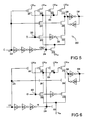
- FIG. 5 is a flip-flop circuit according to one embodiment of the present invention.
- FIG. 6 is an equivalent circuit representation of the circuit of FIG. 5 in its precharge state with the clock signal deasserted.
- FIG. 7 is an equivalent circuit representation of the circuit of FIG. 5 shortly after assertion of the clock signal.
- the invention is generally directed at a flip-flop circuit characterized by symmetrical timing, high performance, low power, and minimized size.
- the circuit includes an output transistor pair that determines that state of the circuit output.
- the output transistor pair is controlled by a first control node when the output is to be driven high and a second control node when the output is to be driven low.
- the first and second control nodes are preferably distinct or decoupled from one another such that capacitive loading associated with the first control node does not affect the second node and vice versa.
- Flip-flop circuit 200 is suitable for use in a wide variety of digital devices.
- Flip-flop circuit 200 is typically implemented as a part of an integrated circuit or module that contains other digital logic to achieve a desired logic design.
- Such an integrated circuit itself typically comprises one of multiple such modules of an electronic device.
- circuit 200 includes n-channel transistors 201 through 205 , p-channel transistors 207 through 210 , a control inverter 215 , a set of pulse width inverters 212 , 214 , and 216 , and a pair of stabilizing inverters 230 and 232 .
- Circuit 200 is configured to receive a clock signal C on a clock input node 222 and a data signal D on a data input node 223 .
- a set of inverters 212 , 214 , and 216 arranged in series, receive the clock signal C and generate a delayed signal CBD, which is a time-delayed, and logically complementary copy of the clock signal) on node 224 .
- the source/drain terminals of p-channel transistors (also referred to as precharge transistors) 207 , 208 , and 209 are connected between a supply voltage Vdd and control node 220 while the gates of these transistors are connected to clock signal C, data signal D, and signal CBD respectively.
- the source/drain terminals of n-channel transistors (also referred to herein as control node transistors) 201 , 202 , and 203 are connected in series between control node 220 and a second supply voltage (Vss or ground) while the gate terminals of these transistors are connected to clock signal C, data signal D, and signal CBD respectively.
- n-channel transistors 205 , 204 , and 203 are connected in series between output node 226 and the second supply voltage while the gate terminals for these transistors are connected to the logical complement of data signal D, clock signal C, and signal CBD respectively.
- the input of control inverter 215 is connected to data node 223 to receive the data input signal D while its output is connected to a second control node 225 , which is connected to the gate terminal of n-channel transistor 205 .
- a first control node 220 of circuit 200 is precharged high, via p-channel transistor 207 , when clock signal C is low as depicted in FIG. 6 .
- p-channel transistor (or first output transistor) 210 and n-channel transistor 204 are both cut-off thereby isolating output node 226 .
- circuit 200 operates as the equivalent circuit depicted in FIG. 7 with p-channel transistors 207 and 209 cut off and n-channel transistors 203 and 204 on.
- control node 220 is tied high by p-channel transistor 208 thereby maintaining p-channel transistor 210 in cut-off. Because control node 220 is precharged high, there is substantially no delay required to transition control node 220 to the high state from the precharge state.
- the low input signal D is inverted by control inverter 215 to turn on n-channel transistor (or second output transistor) 205 thereby completing the path from output node 226 to Vss. In this manner, second output transistor 205 forces output node 226 to a low state (the second state) in response to a low D signal.
- no transition time is required to cut off p-channel transistor 210 . It will be appreciated that the fall time of node 226 is primarily dependent upon the amount of time required to discharge node 226 through the series resistance represented by transistors 203 , 204 , and 205 .
- control node 220 If data signal D is high when the clock signal transitions high, p-channel transistors 207 , 208 , and 209 are all cut-off (until transistor 209 turns back on after the clocking interval) and transistors 201 , 202 , and 203 are turned on thereby permitting control node 220 to discharge and assume a low state. In this state, first output transistor 210 is turned on thereby forcing output node 226 to a high state. The discharge of control node 220 is improved over (faster than) circuit 100 as depicted in FIG. 1 because of reduced capacitive loading on the node.
- first control node 220 of circuit 200 which turns on to force output node to a first state
- second control node 225 which turns on to force output node 226 to a second state
- control node 220 is connected to the gate terminal of just a single transistor (first output transistor 210 )
- This reduction in capacitive loading beneficially improves or reduces the fall time of node 220 and improves the overall performance of circuit 200 .
- the transistor 203 of circuit 200 which replaces a pair of transistors 103 and 106 in circuit 100 of FIG. 1, has a W/L ratio roughly twice that of transistors 201 and 202 .
- the larger ratio of transistor 203 is able to accommodate greater current and represents less resistance in the path between control node 220 and ground. Because the larger transistor 203 replaces a pair of smaller transistors, the reduced resistance is achieved at little or no increase in area.
- circuit 200 achieves more symmetrical output behavior and improved performance in the case where D is high at the cost of just a single additional CMOS inverter ( 215 ).
- the size of this inverter is typically sufficiently small to justify its inclusion in the circuit.
- Circuit 200 beneficially reduces power consumption relative to circuit 100 of FIG. 1 .
- transistors 110 , 104 , 105 , and 106 may all be for a time following a low to high transistor of the clock signal when D is high.
- transistor 104 turns on.
- Transistor 106 remains turned on until CBD transitions low in response to the clock signal going high.
- node 120 With the data signal high, node 120 , which was precharged high, begins to discharge through transistors 101 through 103 .
- Vtp is the threshold voltage of transistor 110
- Transistor 105 does not turn off until control node 120 voltage discharges to Vtn (where Vtn is the threshold voltage of transistor 105 ).
- Vtn is the threshold voltage of transistor 105
- Circuit 200 beneficially eliminates this short circuit current by decoupling the control of transistor 205 from control node 220 .
- transistor 205 is turned off by inverter 215 without regard to the voltage on node 220 thereby preventing the formation of a short circuit current.
- Circuit 200 can be further optimized relative to circuit 100 by appropriate sizing of the transistors.
- transistors 101 through 103 are generally larger (greater W/L) than transistors 104 through 106 to address the asymmetry problem. Larger transistors 101 through 103 reduce the control node 120 discharge time, but result in greater power consumption. Transistors 101 through 103 are generally roughly twice the size of transistors 104 through 106 .
- the capacitance on node 220 is less than the capacitance on node 120 and, therefore, transistors 201 and 202 can be reduced in size relative to transistors 101 and 102 , without negatively affecting performance.
- transistors 201 and 202 have a W/L that is roughly 1.4 times the W/L of transistors 204 and 205 .
- transistors 201 and 202 are small relative to transistors 101 and 102 resulting in reduced power consumption at a comparable performance level.
- circuit 200 further includes an output stabilization circuit comprising a pair of back to back inverters 230 and 232 connected between output node 226 and output node 228 .
- the stabilization circuit compensates for noise that may be present on output node 228 . If noise such as a transient voltage spike is encountered on output node 228 , the stabilization circuit will maintain the state of output node 226 .
Landscapes
- Engineering & Computer Science (AREA)
- Power Engineering (AREA)
- Physics & Mathematics (AREA)
- Computer Hardware Design (AREA)
- Computing Systems (AREA)
- General Engineering & Computer Science (AREA)
- Mathematical Physics (AREA)
- Logic Circuits (AREA)
Abstract
Description
Claims (19)
Priority Applications (1)
| Application Number | Priority Date | Filing Date | Title |
|---|---|---|---|
| US10/255,468 US6825694B2 (en) | 2002-09-26 | 2002-09-26 | Flip-flop circuit for use in electronic devices |
Applications Claiming Priority (1)
| Application Number | Priority Date | Filing Date | Title |
|---|---|---|---|
| US10/255,468 US6825694B2 (en) | 2002-09-26 | 2002-09-26 | Flip-flop circuit for use in electronic devices |
Publications (2)
| Publication Number | Publication Date |
|---|---|
| US20040061531A1 US20040061531A1 (en) | 2004-04-01 |
| US6825694B2 true US6825694B2 (en) | 2004-11-30 |
Family
ID=32029123
Family Applications (1)
| Application Number | Title | Priority Date | Filing Date |
|---|---|---|---|
| US10/255,468 Expired - Fee Related US6825694B2 (en) | 2002-09-26 | 2002-09-26 | Flip-flop circuit for use in electronic devices |
Country Status (1)
| Country | Link |
|---|---|
| US (1) | US6825694B2 (en) |
Cited By (2)
| Publication number | Priority date | Publication date | Assignee | Title |
|---|---|---|---|---|
| US20060001451A1 (en) * | 2004-06-30 | 2006-01-05 | Malik Khurram Z | Dynamic-to-static logic converter |
| US20100207677A1 (en) * | 2009-02-13 | 2010-08-19 | Trivedi Pradeep R | Low latency flop circuit |
Families Citing this family (1)
| Publication number | Priority date | Publication date | Assignee | Title |
|---|---|---|---|---|
| CN105763172B (en) | 2016-02-03 | 2018-07-17 | 中国电子科技集团公司第二十四研究所 | High-speed low-power-consumption trigger |
Citations (2)
| Publication number | Priority date | Publication date | Assignee | Title |
|---|---|---|---|---|
| US5796282A (en) * | 1996-08-12 | 1998-08-18 | Intel Corporation | Latching mechanism for pulsed domino logic with inherent race margin and time borrowing |
| US6496038B1 (en) * | 2000-06-30 | 2002-12-17 | Intel Corporation | Pulsed circuit topology including a pulsed, domino flip-flop |
-
2002
- 2002-09-26 US US10/255,468 patent/US6825694B2/en not_active Expired - Fee Related
Patent Citations (2)
| Publication number | Priority date | Publication date | Assignee | Title |
|---|---|---|---|---|
| US5796282A (en) * | 1996-08-12 | 1998-08-18 | Intel Corporation | Latching mechanism for pulsed domino logic with inherent race margin and time borrowing |
| US6496038B1 (en) * | 2000-06-30 | 2002-12-17 | Intel Corporation | Pulsed circuit topology including a pulsed, domino flip-flop |
Cited By (4)
| Publication number | Priority date | Publication date | Assignee | Title |
|---|---|---|---|---|
| US20060001451A1 (en) * | 2004-06-30 | 2006-01-05 | Malik Khurram Z | Dynamic-to-static logic converter |
| US7098695B2 (en) * | 2004-06-30 | 2006-08-29 | Qualcomm Incorporated | Dynamic-to-static logic converter |
| US20100207677A1 (en) * | 2009-02-13 | 2010-08-19 | Trivedi Pradeep R | Low latency flop circuit |
| US8026754B2 (en) * | 2009-02-13 | 2011-09-27 | Apple Inc. | Low latency flop circuit |
Also Published As
| Publication number | Publication date |
|---|---|
| US20040061531A1 (en) | 2004-04-01 |
Similar Documents
| Publication | Publication Date | Title |
|---|---|---|
| US7405606B2 (en) | D flip-flop | |
| US7973560B2 (en) | Level shifter | |
| US6486719B2 (en) | Flip-flop circuits having digital-to-time conversion latches therein | |
| US20070164789A1 (en) | High Speed Level Shift Circuit with Reduced Skew and Method for Level Shifting | |
| US7583123B2 (en) | High-speed flip-flop circuit | |
| US6853228B2 (en) | Flip-flop circuit | |
| US5889416A (en) | Symmetrical nand gates | |
| US7180326B2 (en) | Noise elimination circuit | |
| US7053662B1 (en) | Method and circuit for high speed transmission gate logic | |
| US6677795B2 (en) | Flip-flop circuit | |
| US6825699B2 (en) | Charge pump circuit, passive buffer that employs the charge pump circuit, and pass gate that employs the charge pump circuit | |
| US11271549B2 (en) | Semiconductor device for controlling voltage at an input node of a circuit during a low power mode | |
| US7528630B2 (en) | High speed flip-flop | |
| US7199638B2 (en) | High speed voltage level translator | |
| US6097222A (en) | Symmetrical NOR gates | |
| US6825694B2 (en) | Flip-flop circuit for use in electronic devices | |
| US6650156B1 (en) | Integrated circuit charge pumps having control circuits therein that inhibit parasitic charge injection from control signals | |
| US5160860A (en) | Input transition responsive CMOS self-boost circuit | |
| US6489815B2 (en) | Low-noise buffer circuit that suppresses current variation | |
| US6407608B1 (en) | Clock input buffer with increased noise immunity | |
| US6323691B1 (en) | Logic circuit | |
| US20060071695A1 (en) | Signal driving circuits including inverters | |
| US6407604B1 (en) | Register and latch circuits | |
| US20260031815A1 (en) | Clock buffer circuit and a semiconductor apparatus using the clock buffer circuit | |
| US7224187B2 (en) | CMOS buffer circuits and integrated circuits using the same |
Legal Events
| Date | Code | Title | Description |
|---|---|---|---|
| AS | Assignment |
Owner name: INTERNATIONAL BUSINESS MACHINES CORPORATION, NEW Y Free format text: ASSIGNMENT OF ASSIGNORS INTEREST;ASSIGNOR:YOO, SEUNG-MOON;REEL/FRAME:013340/0174 Effective date: 20020924 |
|
| FEPP | Fee payment procedure |
Free format text: PAYOR NUMBER ASSIGNED (ORIGINAL EVENT CODE: ASPN); ENTITY STATUS OF PATENT OWNER: LARGE ENTITY |
|
| FPAY | Fee payment |
Year of fee payment: 4 |
|
| REMI | Maintenance fee reminder mailed | ||
| FPAY | Fee payment |
Year of fee payment: 8 |
|
| SULP | Surcharge for late payment |
Year of fee payment: 7 |
|
| AS | Assignment |
Owner name: LEAR CORPORATION, MICHIGAN Free format text: RELEASE BY SECURED PARTY;ASSIGNOR:JPMORGAN CHASE BANK, N.A.;REEL/FRAME:032722/0553 Effective date: 20100830 |
|
| REMI | Maintenance fee reminder mailed | ||
| LAPS | Lapse for failure to pay maintenance fees | ||
| STCH | Information on status: patent discontinuation |
Free format text: PATENT EXPIRED DUE TO NONPAYMENT OF MAINTENANCE FEES UNDER 37 CFR 1.362 |
|
| STCH | Information on status: patent discontinuation |
Free format text: PATENT EXPIRED DUE TO NONPAYMENT OF MAINTENANCE FEES UNDER 37 CFR 1.362 |
|
| FP | Lapsed due to failure to pay maintenance fee |
Effective date: 20161130 |