US6813696B2 - Semiconductor memory device and method of controlling the same - Google Patents
Semiconductor memory device and method of controlling the same Download PDFInfo
- Publication number
- US6813696B2 US6813696B2 US10/694,982 US69498203A US6813696B2 US 6813696 B2 US6813696 B2 US 6813696B2 US 69498203 A US69498203 A US 69498203A US 6813696 B2 US6813696 B2 US 6813696B2
- Authority
- US
- United States
- Prior art keywords
- data
- signal
- input
- clock
- output
- Prior art date
- Legal status (The legal status is an assumption and is not a legal conclusion. Google has not performed a legal analysis and makes no representation as to the accuracy of the status listed.)
- Expired - Lifetime
Links
Images


Classifications
-
- G—PHYSICS
- G11—INFORMATION STORAGE
- G11C—STATIC STORES
- G11C11/00—Digital stores characterised by the use of particular electric or magnetic storage elements; Storage elements therefor
- G11C11/21—Digital stores characterised by the use of particular electric or magnetic storage elements; Storage elements therefor using electric elements
- G11C11/34—Digital stores characterised by the use of particular electric or magnetic storage elements; Storage elements therefor using electric elements using semiconductor devices
- G11C11/40—Digital stores characterised by the use of particular electric or magnetic storage elements; Storage elements therefor using electric elements using semiconductor devices using transistors
- G11C11/401—Digital stores characterised by the use of particular electric or magnetic storage elements; Storage elements therefor using electric elements using semiconductor devices using transistors forming cells needing refreshing or charge regeneration, i.e. dynamic cells
- G11C11/4063—Auxiliary circuits, e.g. for addressing, decoding, driving, writing, sensing or timing
- G11C11/407—Auxiliary circuits, e.g. for addressing, decoding, driving, writing, sensing or timing for memory cells of the field-effect type
- G11C11/409—Read-write [R-W] circuits
-
- G—PHYSICS
- G11—INFORMATION STORAGE
- G11C—STATIC STORES
- G11C7/00—Arrangements for writing information into, or reading information out from, a digital store
- G11C7/10—Input/output [I/O] data interface arrangements, e.g. I/O data control circuits, I/O data buffers
- G11C7/1078—Data input circuits, e.g. write amplifiers, data input buffers, data input registers, data input level conversion circuits
- G11C7/1087—Data input latches
-
- G—PHYSICS
- G11—INFORMATION STORAGE
- G11C—STATIC STORES
- G11C11/00—Digital stores characterised by the use of particular electric or magnetic storage elements; Storage elements therefor
- G11C11/21—Digital stores characterised by the use of particular electric or magnetic storage elements; Storage elements therefor using electric elements
- G11C11/34—Digital stores characterised by the use of particular electric or magnetic storage elements; Storage elements therefor using electric elements using semiconductor devices
- G11C11/40—Digital stores characterised by the use of particular electric or magnetic storage elements; Storage elements therefor using electric elements using semiconductor devices using transistors
- G11C11/41—Digital stores characterised by the use of particular electric or magnetic storage elements; Storage elements therefor using electric elements using semiconductor devices using transistors forming static cells with positive feedback, i.e. cells not needing refreshing or charge regeneration, e.g. bistable multivibrator or Schmitt trigger
- G11C11/413—Auxiliary circuits, e.g. for addressing, decoding, driving, writing, sensing, timing or power reduction
-
- G—PHYSICS
- G11—INFORMATION STORAGE
- G11C—STATIC STORES
- G11C29/00—Checking stores for correct operation ; Subsequent repair; Testing stores during standby or offline operation
-
- G—PHYSICS
- G11—INFORMATION STORAGE
- G11C—STATIC STORES
- G11C29/00—Checking stores for correct operation ; Subsequent repair; Testing stores during standby or offline operation
- G11C29/04—Detection or location of defective memory elements, e.g. cell constructio details, timing of test signals
- G11C29/08—Functional testing, e.g. testing during refresh, power-on self testing [POST] or distributed testing
- G11C29/12—Built-in arrangements for testing, e.g. built-in self testing [BIST] or interconnection details
- G11C29/14—Implementation of control logic, e.g. test mode decoders
-
- G—PHYSICS
- G11—INFORMATION STORAGE
- G11C—STATIC STORES
- G11C7/00—Arrangements for writing information into, or reading information out from, a digital store
- G11C7/10—Input/output [I/O] data interface arrangements, e.g. I/O data control circuits, I/O data buffers
- G11C7/1015—Read-write modes for single port memories, i.e. having either a random port or a serial port
- G11C7/1018—Serial bit line access mode, e.g. using bit line address shift registers, bit line address counters, bit line burst counters
- G11C7/1021—Page serial bit line access mode, i.e. using an enabled row address stroke pulse with its associated word line address and a sequence of enabled column address stroke pulses each with its associated bit line address
-
- G—PHYSICS
- G11—INFORMATION STORAGE
- G11C—STATIC STORES
- G11C7/00—Arrangements for writing information into, or reading information out from, a digital store
- G11C7/10—Input/output [I/O] data interface arrangements, e.g. I/O data control circuits, I/O data buffers
- G11C7/1015—Read-write modes for single port memories, i.e. having either a random port or a serial port
- G11C7/1039—Read-write modes for single port memories, i.e. having either a random port or a serial port using pipelining techniques, i.e. using latches between functional memory parts, e.g. row/column decoders, I/O buffers, sense amplifiers
-
- G—PHYSICS
- G11—INFORMATION STORAGE
- G11C—STATIC STORES
- G11C7/00—Arrangements for writing information into, or reading information out from, a digital store
- G11C7/10—Input/output [I/O] data interface arrangements, e.g. I/O data control circuits, I/O data buffers
- G11C7/1051—Data output circuits, e.g. read-out amplifiers, data output buffers, data output registers, data output level conversion circuits
- G11C7/1066—Output synchronization
-
- G—PHYSICS
- G11—INFORMATION STORAGE
- G11C—STATIC STORES
- G11C7/00—Arrangements for writing information into, or reading information out from, a digital store
- G11C7/10—Input/output [I/O] data interface arrangements, e.g. I/O data control circuits, I/O data buffers
- G11C7/1072—Input/output [I/O] data interface arrangements, e.g. I/O data control circuits, I/O data buffers for memories with random access ports synchronised on clock signal pulse trains, e.g. synchronous memories, self timed memories
-
- G—PHYSICS
- G11—INFORMATION STORAGE
- G11C—STATIC STORES
- G11C7/00—Arrangements for writing information into, or reading information out from, a digital store
- G11C7/10—Input/output [I/O] data interface arrangements, e.g. I/O data control circuits, I/O data buffers
- G11C7/1078—Data input circuits, e.g. write amplifiers, data input buffers, data input registers, data input level conversion circuits
- G11C7/1096—Write circuits, e.g. I/O line write drivers
-
- G—PHYSICS
- G11—INFORMATION STORAGE
- G11C—STATIC STORES
- G11C7/00—Arrangements for writing information into, or reading information out from, a digital store
- G11C7/22—Read-write [R-W] timing or clocking circuits; Read-write [R-W] control signal generators or management
- G11C7/222—Clock generating, synchronizing or distributing circuits within memory device
Definitions
- the present invention relates to a semiconductor memory device in synchronization with an external clock signal and its control method, and relates in particular to synchronous DRAM (Synchronous Dynamic Random Access Memory: SDRAM) which reads or writes data synchronously with the external clock signal and its control method for writing data.
- SDRAM Synchronous Dynamic Random Access Memory
- the conventional DRAM inputs or outputs data independently (Asynchronous) from the clock signal supplied to a system, thereby preventing the input of following addresses until the data corresponding to the address is output from an address input.
- the cycle time of a data transfer depends upon the access time up to the data output, thus causing a difficulty in the improvement of data transfer rate.
- MPU processing unit
- PC personal computer
- SDRAM with the column access path divided into several pipelines and the read/write process between each pipelines synchronized with the rising edge of the external clock signal supplied from the system side has been developed. Furthermore, with no change in the basic architecture of the circuit, a SDRAM in DDR mode (Double Data Rate) which inputs or outputs the data synchronously with both the rising and falling edges of the external clock signal (CLK) is developed (for example, described in particular in Japanese Application No. 9-167451, Japanese Application No.
- DDR mode Double Data Rate
- the data transfer rate of the SDRAM in the DDR mode has an advantage of being approximately twice as fast as that of the SDRAM in which the data is synchronized in transmission only with the rising edge of the external clock signal (hereinafter called SDR mode for convenience), thus becoming the present mainstream of the SDRAM.
- the memory test equipment includes counting the number of defective memory cells and judging whether the repair of the defective memory cells is feasible under a situation identical to the normal operative condition. For example, in testing for the defective memory cells in the SDRAM, the memory test equipment generates a signal identical to the external clock signal CLK used during the actual operation of the SDRAM and input it to the SDRAM. It should be noted that a wafer test checks all chips formed on a semiconductor wafer and tests writing and reading of the predetermined data to each chip.
- the above-mentioned SDRAM having the DDR mode is quite different from the SDRAM having the conventional SDR mode in operations.
- the DDR mode since the DDR mode generates the write/read data in frequency twice that of the conventional type, it is required to newly introduce the memory test equipment which can generate the clock signal for a test corresponding to the DDR mode.
- This in turn requires the purchase of new memory test equipment for manufacturing SDRAM in the DDR mode, so resulting in higher investment in equipment and increasing the cost of the SDRAM having the DDR mode.
- the inability of using the conventional memory test equipment causes a delay in product development of the DDR mode SDRAM.
- FIG. 21 is a timing chart showing a comparison between the data reading tests in the wafer test of the semiconductor memory device regarding to an embodiment of the prior and present inventions.
- FIG. 22 is a timing chart showing a comparison between the data writing tests in the wafer test of the semiconductor memory device regarding to an embodiment of the prior and present inventions.
- FIG. 21 ( a ) and FIG. 22 ( a ) are the timing charts of the data reading and data writing tests of the SDRAM in the DDR type which is a conventional semiconductor memory device
- FIG. 21 ( b ) and FIG. 22 ( b ) are the timing charts of the data reading and data writing tests of the SDRAM of the DDR type which is a semiconductor memory device as an embodiment of the present invention later described.
- the completion of a series of data readings requires a time equivalent to 13 clk's after an active state.
- testing by operating the device with a half the frequency of the actual semiconductor tester like this leads to a problem to introduce an increase in manufacturing cost.
- testing the SDRAM of the DDR type under the ordinary operation requires expensive test equipment that has a frequency band twice as fast as the operation speed of the SDRAM, which consequently increases the manufacturing cost of the SDRAM of the DDR type significantly.
- Use of the ordinary test equipment requires all device clocks CLK to be operated with a half the frequency of the tester clock clk and a redundant timing must be set in all tests. Consequently, the test time becomes longer and also the manufacturing cost of the devices is increased.
- An object of the present invention is to provide a semiconductor memory device that can be easily tested and evaluated by the conventional memory test equipment and its control method, while having a transfer mode to transfer data in synchronization with the rising and falling edges of the external clock.
- a further object of the present invention is to provide a semiconductor memory device that can reduce the test time without the use of expensive test equipment.
- a semiconductor memory device operable in synchronization with an external clock signal comprising a data transfer circuit, having a first transfer mode and a second transfer mode, for transferring data in synchronization with rising and falling edges of an external clock signal in the first transfer mode, and for transferring data in synchronization with only one of the rising and falling edges in the second transfer mode.
- the data transfer circuit switches the first and second transfer modes in response to a mode switch signal.
- the conventional memory test equipment can be used to test and evaluate the semiconductor memory device by switching to the second transfer mode. In an actual use, it is also possible to realize a high-speed data transfer rate by switching to the first transfer mode.
- the mode switch signal is generated on the basis of a setting signal input from outside the device. Furthermore, the semiconductor memory device of the present invention has a register to latch the setting signal. By forming such a structure, the transfer mode of the data transfer circuit can easily be switched from the system side which utilizes the semiconductor memory device.
- an empty register in a mode register can be used as the register. It is possible to easily maintain the mode switch signal by utilizing the empty register of the mode register arranged also in the conventional SDRAM. Or, by arranging a switch signal input terminal to the semiconductor memory device of the present invention and by inputting a mode switch signal from the system side to the switch signal input terminal, the transfer mode of a direct data transfer circuit may be switched from the system side. By doing like this, the circuit structure of the semiconductor memory device can be more simply formed.
- the second transfer mode may transfer data in synchronization with the rising and falling edges of the external clock signal. By doing this, the transfer rate of half that of the first transfer mode can be realized with a duty ratio of the external clock equal to 50%.
- the data transfer circuit has a data input converter, for simultaneously transferring parallel data converted from serial data which are input serially in the first transfer mode, and for sequentially transferring the serial data in the second transfer mode.
- the data transfer circuit has a data input clock generating circuit, for generating a first clock signal in the first transfer mode or a second clock signal in the second transfer mode in response to the mode switch signal, and for transmitting the first clock signal or the second clock signal to the data input converter.
- a data input operation at the data input converter in the first or second transfer mode can be easily changed by a simple circuit structure.
- the data transfer circuit has a write control circuit, for generating a first write enable signal to simultaneously transfer the parallel data to a memory cell array in the first transfer mode, and for generating a second write enable signal to sequentially transfer the serial data to the memory cell array in the second transfer mode.
- a write enable signal in response to the first and second transfer modes are output on the basis of the mode switch signal, data can surely be transferred in both of the first and second transfer modes in synchronization with a data input converter which executes a data input operation by the clock signal on the basis of the mode switch signal also.
- the semiconductor memory device comprises a column address counter which can change a timing to count up a column address in response to the mode switch signal.
- a column address counter of the present invention comprises a clock generating circuit supplying a first internal address generating clock and a second internal address generating clock, a first address generating section generating a first internal address in synchronization with the first internal address generating clock, and a second address generating section generating a second internal address in synchronization with the second internal address generating clock.
- the clock generating circuit comprises a clock generator and a frequency divider, the clock generator generating an internal clock in response to the external clock, the frequency divider receiving the internal clock and generating a divided clock, and wherein the clock generating circuit outputs the internal clock as the first internal address generating clock in the first transfer mode, and outputs the divided clock as the first internal address generating clock and the internal clock as the second internal address generating clock in the second transfer mode.
- the semiconductor memory device of the present invention also comprises a burst counter which starts counting the internal clock according to a write or read command, and deactivates the clock generator signal when the predetermined number of the internal clocks is counted. Furthermore, the burst counter comprises a burst length conversion circuit for converting the predetermined number of the internal clocks in response to the mode switch signal.
- the data transfer circuit transfers data to a memory cell array when the data is the write data.
- the reason of the data write failure is easily analyzed using the conventional test equipment particularly by switching the first transfer mode to the second transfer mode when data are written.
- a control method of the semiconductor memory device operable in synchronization with an external clock signal comprising transferring data in synchronization with both of rising and falling edges of the external clock signal in a first transfer mode, and transferring the data in synchronization with one of the rising and falling edges in a second transfer mode.
- this control method since it is possible to switch to the second transfer switch in the test of the semiconductor memory device, the failure analysis of the memory cells is easily made by using the conventional memory test equipment.
- the first transfer method which can realize a high-speed data transfer rate can be employed in the actual use of the semiconductor memory device.
- the first and second transfer modes are switched in response to a switch signal which is generated on the basis of a setting signal input from outside of the device or directly input from the outside. Also, the data is transferred in synchronization with the rising edge of the external clock signal in the second transfer mode. Further, in this control method, in the first transfer mode, a plurality of data serially input are converted from serial data to parallel data and the converted parallel data are simultaneously transferred. In the second transfer mode, a plurality of data are sequentially transferred.
- the step of transferring includes outputting a first write enable signal to a write amplifier in the first transfer mode and outputting a second write enable signal in the second transfer mode in response to a switch signal when the data is transferred to a memory cell array. Furthermore, in the control method of the semiconductor memory device of the present invention, a timing to count up a column address is changed in response to the switch signal.
- the second transfer mode is selected when the data is written in a test mode.
- a semiconductor memory device of a double data rate type for reading the data in response to rising and falling edges of a clock having an operating mode to immediately read the data with a read command.
- a semiconductor memory device of a double data rate type for writing data in response to both of rising and falling edges of a clock having an operating mode for immediately writing the data after a write command is received.
- a semiconductor memory device of a double data rate type for writing data in response to both of rising and falling edges of a clock having a single data rate mode to write data in response to one of the rising and falling edges of the clock.
- the semiconductor memory device of the present invention has not only the double data rate mode but also a mode to read data immediately with a write command.
- the semiconductor memory device of the present invention has not only the double data rate mode but also the single data rate mode to read data in response to one of the rising and falling edges of a clock.
- the semiconductor memory device of the present invention has not only the double data rate mode but also a mode to write data immediately with a write command.
- the semiconductor memory device of the present invention has not only the double data rate mode but also the single data rate mode to write data in response to one of rising or falling edges of a clock.
- a semiconductor memory device capable of reducing a test time can be provided without the use of expensive test equipment.
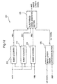
- FIG. 1 is a block diagram showing a total structure of the semiconductor memory device in the first embodiment of the present invention.
- FIG. 2 is a table describing an example of commands that are generated at a command decoder of the semiconductor memory device in the first embodiment of the present invention.
- FIG. 3 is a block diagram showing a structure of a data input clock generating section and a write amplifier control section of the semiconductor memory device in the first embodiment of the present invention.
- FIG. 4 is a circuit diagram showing an example of a circuit structure which has a data input clock generating section, a serial/parallel conversion section, and a write amplifier control section of the semiconductor memory device in the first embodiment of the present invention.
- FIG. 5 is a timing chart showing a control method of a write operation in the DDR mode of the semiconductor memory device in the first embodiment of the present invention.
- FIG. 6 is a timing chart showing a control method of a write operation in the SDR mode of the semiconductor memory device in the first embodiment of the present invention.
- FIG. 7 is a circuit block diagram of a column address counter of the semiconductor memory device in the first embodiment of the present invention.
- FIG. 8 is a timing chart showing a control method of an operation of the column address counter of the semiconductor memory device in the first embodiment of the present invention.
- FIG. 9 is a diagram showing a circuit example of a clock generating section in the column address counter of the semiconductor memory device in the first embodiment of the present invention.
- FIG. 10 is a diagram showing a circuit example of a 1 ⁇ 2-frequency divider and a clock switch section in the column address counter of the semiconductor memory device in the first embodiment of the present invention.
- FIG. 11 is a timing chart showing an operation of the clock generation section in the column address counter of the semiconductor memory device in the first embodiment of the present invention.
- FIG. 12 is a diagram showing a circuit block in a burst counter of the semiconductor memory device in the first embodiment of the present invention.
- FIG. 13 is a diagram showing a circuit example in a burst counter of the semiconductor memory device in the first embodiment of the present invention.
- FIG. 14 is a diagram showing a circuit example in a burst counter of the semiconductor memory device in the first embodiment of the present invention.
- FIG. 15 is a timing chart showing an operation of the burst counter of the semiconductor memory device in the first embodiment of the present invention.
- FIG. 16 is a diagram showing a circuit block of an address generating section of the semiconductor memory device in the first embodiment of the present invention.
- FIG. 17 is a diagram showing a circuit example of an A 0 generating section in the address generating section of the semiconductor memory device in the first embodiment of the present invention.
- FIG. 18 is a diagram showing a circuit example of an A 1 generating section in the address generating section of the semiconductor memory device in the first embodiment of the present invention.
- FIG. 19 is a diagram showing a circuit example of an A 2 generating section in the address generating section of the semiconductor memory device in the first embodiment of the present invention.
- FIG. 20 is a diagram showing a circuit example of a carry decision section in the address generating section of the semiconductor memory device in the first embodiment of the present invention.
- FIG. 21 is a timing chart showing a comparison between data read tests in the semiconductor memory device in the second embodiment of the prior and present invention.
- FIG. 22 is a timing chart showing a comparison between data write tests in the semiconductor memory device in the second embodiment of the prior and present invention.
- FIG. 23 is a block diagram (first) showing an example of the read circuit of the semiconductor memory device in the second embodiment of the present invention.
- FIG. 24 is a block diagram (second) showing an example of a read circuit of the semiconductor memory device in the second embodiment of the present invention.
- FIG. 25 is a timing chart describing a read operation in the DDR mode in the semiconductor memory device in the second embodiment of the present invention.
- FIG. 26 is a timing chart describing a read operation in the SDR mode in the semiconductor memory device in the second embodiment of the present invention.
- FIG. 27 is a circuit diagram showing an example of an output data latch and an output data buffer at an output section in the semiconductor memory device in the second embodiment of the present invention.
- FIG. 28 is a block diagram (first) showing an example of a write circuit of the semiconductor memory device in the second embodiment of the present invention.
- FIG. 29 is a block diagram (second) showing an example of a write circuit of the semiconductor memory device in the second embodiment of the present invention.
- FIG. 30 is a block diagram (third) showing an example of a write circuit of the semiconductor memory device in the second embodiment of the present invention.
- FIG. 31 is a timing chart describing a write operation in the DDR mode in the semiconductor memory device in the second embodiment of the present invention.
- FIG. 32 is a timing chart explaining the write operation in the SDR mode in the semiconductor memory device in the second embodiment of the present invention.
- FIG. 33 is a circuit diagram showing an example of an input data latch and an address latch at the input section in the semiconductor memory device in the second embodiment of the present invention.
- FIG. 34 is a. block diagram showing a total structure of a transformation example of the semiconductor memory device in the second embodiment of the present invention.
- the first embodiment describes a structure, in a data write operation, which operates in the DDR type during the ordinary operation and can operate in the SDR type during the test operation.
- a schematic structure of the semiconductor memory device in the first embodiment is described with reference to a system block diagram shown in FIG. 1 .
- the semiconductor memory device in the first embodiment comprises a basic structure of the SDRAM that operates in the DDR mode.
- an inside of the SDRAM 1 is divided into two banks (bank 0 and bank 1 ) where each can be controlled independently.
- the SDRAM 1 in the first embodiment has two banks 0 and 1 , actually a plurality of banks (for example, four banks) can be provided of course.
- the banks 0 and 1 have the same circuit structure. For example, if they are 16 Mb SDRAM's, the same situation as operating two independent two 8 Mb DRAM's can be made.
- a memory cell section 2 in which memory cells consisting of a transistor for a transfer gate and a capacitor (both are omitted in the diagrams) are arranged in the matrix. Also, a row selection line (word line) and a bit line extending to the direction of the row and column are formed between each memory cells at the memory cell section 2 .
- a gate electrode of the transistor in each memory cell arranged in the same direction of the row is connected to the same row selection line, and a drain electrode of the transistor in each memory cells arranged in the same direction of the column is connected to the same bit line.
- a plurality of these row selection lines are driven by a row decoder 4
- a plurality of column selection lines which control a column gate between the bit line and a data bus 10 are driven by a column decoder 6 .
- a sense amplifier 8 is provided to output an amplified signal existing at the paired bit lines.
- a data bus 10 is connected to a write amplifier/sense buffer 12 .
- data which are output to the data bus 10 are controlled on the basis of a write control signal WE from a write amplifier control section (write control section) 14 .
- WE write amplifier control section
- the data of the memory cell selected at a desired row selection line is amplified at a sense amplifier and is output to the data bus 10 via a column gate which is controlled by the desired column selection line.
- data on the data bus 10 is written to the sense amplifier 8 and amplified, and then written to the predetermined memory cell.
- SDRAN 1 has a clock buffer 16 , a command decoder 18 , an address buffer/register & bank select 20 , an I/O data buffer/register 22 , control signal latch circuits 24 and 26 , a mode register 28 , and column address counters 30 , and 32 .
- An external clock signal CLK and a clock enable signal CKE are supplied to the clock buffer 16 externally.
- the clock buffer 16 generates a clock signal CLK 0 ° in synchronization with the rising edge of the external clock signal CLK, while it generates a clock signal CLK 180 ° in synchronization with the falling edge of the external clock signal CLK.
- the clock buffer 16 controls the supply of the clock signal CLK 0 ° and the clock signal CLK 180 ° to each circuit of the SDBAM 1 on the basis of the level of a clock enable signal CRE.
- the clock enable signal CKE is supplied from the clock buffer 16 to each of the command decoder 18 , the address buffer/register & bank selector 20 , and a data input clock generator 34 in the I/O data buffer/register 22 .
- the command decoder 18 decodes a chip select signal/CS, a row address strobe signal/RAS, a column address strobe signal/CAS, and a write enable signal/WE, thus generating a variety of control signals (command) controlling the operation of the SDRAM 1 by combinations of these signals.
- “/” shows that each signal is activated with a signal level being low.
- the generated control signals are input to the control signal latch circuits 24 and 26 , the column address counter 30 , the mode register 28 , and so on.
- FIG. 2 shows a command function name, a command name, the state of the clock enable signal CKE, the chip select signal/CS, the row address strobe signal/RAS, the column address strobe signal/CAS, each state of the write enable signal/WE, and the state of each bit of addresses A 0 ⁇ A 11 which will be described later.
- “H” shows a high level
- “L” shows a low level
- “X” shows a high or low level
- V shows a definite input
- n shows a state in the present clock cycle
- n ⁇ 1 shows a state one cycle previous.
- the I/O data buffer register 22 inputs or outputs the write/read data between either bank 0 or bank 1 , and it has 32 bit parallel data lines respectively for writing or reading to write the data to the memory cell section or to read the data from the memory cell section 2 .
- the data lines are connected to each of the write amplifier/sense buffer 12 in the banks 0 and 1 after diverging on the way.
- the I/O data buffer/register 22 has the data input clock generating section 34 as will be described later.
- control signal latch circuits 24 and 26 After receiving the control signal (command) described before from the command decoder 18 , based on it, the control signal latch circuits 24 and 26 generate a various internal control signals (RAS, CAS, WE, and so on) and output them to banks 0 and 1 . As has been described before, the write control signal WE output from the signal latch circuit 24 is input to the write amplifier control section 14 in the bank 0 .
- the mode register 28 has a register consisting of 12 bits of A 0 ⁇ A 11 , and therefore can set the data length (burst length: for example, 1, 2, 4, or 8) sequentially accessing during a burst mode which will be described later, a burst type in a sequential mode or in an interleave mode, or a CAS latency which outputs the data with delay of the predetermined number of clocks (for example, 1, 2, or 3 clocks) from the receiving time of the read (READ) command during the burst transfer mode.
- a 0 ⁇ A 2 are used for setting the burst length
- a 3 is used for setting the burst type
- a 4 ⁇ A 6 are used for setting the CAS latency.
- the setting of the mode register 28 is described with reference to FIG. 2 .
- the clock enable signal CKE (n ⁇ 1) is “H” and CKE(n) is “X”.
- the chip select signal/CS, the row address strobe signal/RAS, the column address strobe signal/CAS and the write enable signal/WD are all “L”, Furthermore, when the addresses A 0 -A 10 are “V′1 and address A 11 is “L”, a mode register set (MRS) command is generated to set the data to the registers A 0 -A 11 of the mode register 28 .
- MRS mode register set
- the mode register 28 When the generated MRS command is executed, the mode register 28 receives the signal A 0 -A 11 for setting the mode register 28 which is input to the address buffer/register & bank select 20 as the setting signal input from the external, thereby setting its own register A 0 -A 11 . With this, the settings of the predetermined burst length, the burst type and the CAS latency are completed.
- the mode register 28 in the embodiment 1 uses, for example, the bit A 11 as a register to switch and set the SDRAM 1 to one of the DDR mode and SDR mode when the data is written. If the bit A 11 is “0”, the data write operation of the SDRAM 1 is set to the DDR mode, and if it is “1”, the operation is set to the SDR mode.
- the mode register 28 outputs a DDR signal (switch signal), which shows one of the DDR or SDR mode, to the column address counters 30 and 32 along with outputting the set burst length, the burst type, and information of the CAS latency to the column address counters 30 and 32 .
- the mode register 28 also transmits the DDR signal to the data input clock generating section 34 in the I/O data buffer/register 22 and to the write amplifier control section 14 in the banks 0 and 1 .
- a data transfer circuit which can be used by switching the DDR mode and the SDR mode at least by the I/O data buffer/register 22 and the write amplifier control section 14 is formed.
- the mode register 28 is an example of the switching means to switch the data transfer circuit to either the DDR or SDR mode.
- the column address counters 30 and 32 are counters to sequentially increment the column address of the data write/read in the burst mode.
- the column address counters 30 and 32 count up the column address received from the address buffer/register & bank selector 20 in synchronization with the clocks CLK 0 ° and CLK 180 ° supplied from the clock buffer 16 , thereby making it possible to read or write the sequential address data.
- the transfer type of the data using the column address counters 30 and 32 is referred to a burst mode.
- the column addresses whose number is the same as that of the data sequentially input or output are generated and supplied to the banks 0 and 1 at each predetermined clock, on the basis of the burst length set to the mode register 28 .
- FIG. 3 shows, when the data is written, the I/O data buffer/register 22 , signals supplied to the write amplifier control section 14 and to the write amplifier in the write amplifier/sense buffer 12 in the bank 0 , and the flow of signals supplied.
- FIG. 3 shows an operation to process either one bit of a bundle of data DQ 0 -DQn input to the I/O data buffer/register 22 , the whole processing of the data DQ 0 -DQn consisting of actual n+1 bits can also be executed in the same way.
- the I/O data buffer/register 22 comprises the above-mentioned data input clock generating section 34 , a data input latch circuit 36 , and serial/parallel conversion section 38 which is a data input/output conversion section.
- the pulses of the clock signals CLK 0 ° and CLK 180 ° generated at the clock buffer 16 and the DDR signal from the mode register 28 inputs to the data input clock generating circuit 34 .
- the three kinds of signals consisting of a clock signal CLK-A, a clock signal-B, and a clock signal-C are generated at the data input clock generating section 34 , where the CLK-A is formed by synthesizing the clock signal CLK 0 ° and the clock signal CLK 180 °.
- the CLK-B is formed on the basis of the clock signal CLK 0 °
- the CLK-C is formed on the basis of the clock signal CLK 180 °.
- the generated clock signal cLK-A is input to the data input latch circuit 36 , thereby controlling the external data DQ which input to the data input latch circuit 36 .
- output signals S 2 and S 3 controlled by the clock signals CLK-B and CLK-C are output to write amplifiers 40 and 42 in the bank 0 at the serial/parallel conversion section 38 .
- the signal S 2 which is a DQ( FIRST ) previously input to the data input latch circuit 36 , is input to the write amplifier 40 .
- the signal S 3 which is a DQ( SECOND ) in turn input to the data input latch circuit 36 , is input to the write amplifier 42 .
- the write command WE generated at the command decoder 18 is input to the write amplifier control section 14 in the bank 0 through the control signal latch circuit 24 , and the pluses of the clock signals CLK 0 ° and CLK 180 ° from the clock buffer 16 and the DDR signal from the mode register 28 are input.
- the write amplifier control section 14 simultaneously sets the write control signals WE 1 and WE 2 “H” to the write amplifiers 40 and 42 with the predetermined interval on the basis of the clock signals CLK 0 ° and CLK 180 °.
- the write amplifiers 40 and 42 output the signals S 2 as data DB 0 and /DB 0 and S 3 as data DB 1 and /DB 1 respectively to the side of the memory cell section 2 during the write control signals WE 1 and WE 2 are “H”.
- the period in which the write control signals WE 1 and WE 2 are “H” is actually a data input definite period, and therefore the data can be written.
- the data DQ( FIRST ) and DQ( SECOND ) which are input sequentially to the data input latch circuit 36 are converted at a serial/parallel conversion section 38 , and thereby the 2 data of DQ( FIRST ) and DQ( SECOND ) can be simultaneously output to the write amplifiers 40 and 42 respectively.
- the clock signals CLK-B and CLK-C are fixed at “H” level not to generate a pulse at the data input clock generating section 34 , so that the period of the signals S 2 and S 3 are defined only by the clock signal CKL-A which inputs to the data input latch circuit 36 .
- the write amplifier control section 14 in case the DDR signal from the mode register 28 is “L”, alternatively sets the write control signals WE 1 and WE 2 to the write amplifiers 40 and 42 as “H” at the predetermined interval on the basis only of the clock signal CLK 0 °. Therefore, the data Db 0 and /Db 0 , and DB 1 and /DB 1 can be alternatively output from the write amplifiers 40 and 42 to the side of the memory cell section 2 with a cycle twice as long as that in the DDR mode. This is equivalent to executing the same SDR operation as the conventional SDRAM.
- the test and evaluation can be made by the use of the memory test equipment corresponding only to the conventional SDR mode without buying and preparing new memory test equipment for the SDRAM which operates in the DDR mode having a clock frequency twice as high as the conventional one as the memory test equipment to use for the circuit evaluation.
- the memory test equipment can be used together with the one for the conventional SDRAM, so that the burden of the test evaluation can be reduced and an increase in investment for the equipment can be suppressed.
- Two three-input NAND circuits 50 and 52 are provided at the side of the signal input of the data input clock-generating section 34 .
- the clock signal CLK 0 ° and the write command WE are input to two-input terminals of the NAND circuit 50 and the rest of the input terminals are continuously maintained in the “H” state.
- the clock signal CLK 180 °, the write command WE, and the DDR signal are input.
- the DDR signal is input to an inverter 62 .
- An output terminal of the NAND circuit 50 is connected to an inverter 56 and to one of the input terminals of the two-input NAND circuit 54 , while an output terminal of the NAND circuit 52 is connected to an inverter 60 and to the other terminal of the two-input NAND circuit 54 .
- An output of the NAND circuit 54 is input to the data input latch circuit 36 in the I/O data buffer/register 22 as the clock signal CLK-A.
- An output terminal of the inverter 56 is connected to one of the input terminals of a two-input NOR circuit 66 , while one of the terminals of a capacitor 58 for the signal delay is connected between the inverter 56 and the NOR circuit 66 .
- the other terminal of the capacitor 58 is, for example, maintained at the ground potential.
- an output terminal of the inverter 60 is connected to one of the input terminals of a two-input NOR circuit 68 , while one of the terminals of a capacitor 64 for the signal delay is connected between the inverter 60 and the NOR circuit 68 .
- the other terminal side of the capacitor 64 is, for example, maintained at the ground potential.
- To the other terminals of the two-input NOR circuits 66 and 68 the output terminal of the inverter 62 are respectively connected.
- An output terminal of the NOR circuit 66 is connected to an input terminal of an inverter 70 and then an output of the inverter 70 is input to the serial/parallel conversion section 38 in the I/O data buffer/resister 22 as the clock signal CLK-B.
- an output terminal of the NOR circuit 68 is connected to the input terminal of an inverter 72 , while an output of the inverter 72 is input to the serial/parallel conversion section 38 in the I/O data buffer/register 22 as the clock signal CLK-C.
- the SDRAM 1 when the DDR signal and the write command WE becomes “H” state, in short, the SDRAM 1 is in a mode to execute the write operation in the DDR type, the output of the NAND circuit 50 becomes “L” when the clock signal CLK 0 ° becomes “H”, and “H” when the clock signal CLK 0 ° becomes “L”.
- the output of the NAND circuit 52 becomes “L” when the clock signal CLK 180 ° becomes “H”, and “H” when the clock signal CLK 0 ° becomes “L”.
- the clock signal CLK-A synchronizing with both the rising and falling edges of the external clock signal CLK is output as a synthesized signal of the clock signal CLK 0 ° and clock signal CLK 180 ° at the output of the NAND circuit 54 whose two inputs are outputs from the NAND circuits 50 and 52 .
- a signal which has converted the output of the NAND circuit 50 through the inverter 56 is input to one of the input terminals of the NOR circuit 66 and a signal at “L” level which has converted the DDR signal through the inverter 62 is input to the other of the input terminals of the NOR circuit 66 . Therefore, a signal which has converted the clock signal CLK 0 ° is output from the NOR circuit 66 .
- an output of the NOR circuit 66 becomes a signal output which is delayed the predetermined time from the clock signal CLK 0 ° by the capacitor 58 operating as a signal delay circuit.
- This signal is input to the inverter 70 to be converted, and the clock signal CLK-B of a like-pole with the predetermined phase shift from the clock signal CLK 0 ° is output from the inverter 70 .
- NOR circuit 68 a signal which has converted the output of the NAND circuit 52 through an inverter 62 is input to one of the input terminals of the NOR circuit 68 and a signal at “L” level which has converted the DDR signal through the inverter 62 is input to the other terminal. Therefore, a signal which has converted the clock signal CLK 180 ° is output from the NOR circuit 68 . At this time, the output of the NOR circuit 68 becomes a signal output delayed the predetermined time from the clock signal CLK 180 ° by the capacitor 64 operating as a signal delay circuit. This signal is input to an inverter 72 to be converted and the clock signal CLK-C of a like-pole with the predetermined phase shift from the clock signal CLK 180 ° is output from the inverter 72 .
- a signal in synchronization with the clock signal CLK 0 °, in short, the clock signal CLK-A in synchronization with the rising edge of the external clock signal CLK, is output from the output of the NAND circuit to which the outputs from these NAND circuits 50 and 52 are input.
- NOR circuit 66 a signal converted from the output of the NAND circuit 50 through the inverter 56 is input to one of the input terminals of the NOR circuit 66 and a signal at “H” level converted from the DDR signal through the inverter 62 is input to the other terminal. Therefore, the output of the NOR circuit 66 continuously becomes “L”, and the clock signal CLK-B which is continuously maintained “H” after inputting to and converted by the next stage inverter 70 is output. Similarly, when the DDR signal is “L”, the clock signal CLK-C continuously maintained at “H” is output also from the NOR circuit 68 .
- FIG. 5 shows the timings (burst length is 8) of the write operation of the SDRAM 1 when the DDR signal is “H”.
- FIG. 6 shows timings (burst length is 4) of the write operation of the SDRAM 1 when the DDR signal is “L”. In the write operation in the DDR mode as shown in FIG.
- the clock signal CLK-A is generated by synthesizing both of the clock signals CLK CLK 0 ° and CLK 180 °
- the clock signal CLK-B is generated from the clock signal CLK 0 ° with the predetermined time delay
- the clock signal CLK-C is generated from the clock signal CLK 180 ° with the predetermined time delay.
- the clock signal CLK-A is generated on the basis of the clock signals CLK CLK 0 °, thereby maintaining the clock signal CLK-B and CLK-X at “H”.
- the write data (DQ) transferred from the data lines (omitted in FIG. 4) connected to a pad (pad) is input to the data input latch circuit 36 .
- the data input latch circuit 36 latches the DATA DQ in synchronization with the clock signal CLK-A input from the data input clock generating section 34 , and then transfers it to the serial/parallel conversion section 38 as a signal S 1 .
- the serial/parallel conversion section 38 has a latch circuit 82 consisting of two inverters 84 and 86 , where one output is the input for the other to latch the signal S 1 from the data input latch circuit 36 . Also, the signal S 1 is input also to a latch circuit 88 consisting of inverters 90 and 92 through a transfer gate circuit 74 .
- the transfer gate circuit 74 is formed by connecting a n-channel MOSFET 76 and p-channel MOSFET 78 in parallel, where ON/OFF of the n-channel MOSFET 76 is controlled by the level of the clock signal CLK-B and ON/OFF of the p-channel MOSFET 78 is controlled according to the output from an inverter 80 reversing the level of the clock signal CLK-B. Therefore, when the clock signal CLK-B becomes “H”, the n-channel MOSFET 76 and p-channel MOSFET 78 become ON state, and the signal flows to the transfer gate circuit 74 .
- a transfer gate circuit 94 consisting of an n-channel MOSFET 98 and p-channel MODFET 96 is provided at the next stage of the latch circuit 82 . Also, at the next stage of the latch circuit 88 , a transfer gate circuit 100 consisting of an n-channel MODFET 102 and a p-channel MOSFET 104 is provided.
- the clock signal CLK-C is input to the gate of the n-channel MODFET's 98 and 102 in the transfer gate circuits 94 and 100 , and ON/OFF is controlled by the level of the clock signal CLK-C. Also, the clock signal CLK-C is reversed at an inverter and then input to the gate of the p-channel MOSFET's 96 and 104 in the transfer gate circuits 94 and 104 . So that, when the clock CLK-C become “H”, a signal flows to the transfer gates 94 and 100 , thereby cutting off the signal at the transfer gates 94 and 100 .
- Latch circuits 108 and 114 are respectively provided at the next stage of the transfer gate circuits 94 and 100 .
- the latch circuit 108 has two inverters 100 and 112 in which one output is the input for the other and this maintains the data maintained at the latch circuit 82 as the signal S 3 when it is input through the transfer gate circuit 94 .
- the latch circuit 114 has two inverters 116 and 118 in which one output is the input for the other, also maintaining the data maintained at the latch circuit 88 as the S 2 when they are input through the transfer gate circuit 100 .
- the signal S 2 maintained at the latch circuit 114 is output to the write amplifier 40 in the bank 0 .
- the signal S 3 maintained at the latch circuit 108 is output to the write amplifier 42 .
- a write operation of the serial/parallel conversion section 38 having the above circuit structure, when the DDR signal and the write command WE are in “H” state, in short, when the SDRAM 1 is in the DDR mode, is described with reference to FIG. 4 and FIG. 5 .
- the data D 0 inputs to the data input latch circuit 36 through the data pad, and then latches at the rising edge of the clock signal CLK-A.
- the next data D 1 is latched at the rising edge of the clock signal CLK-A and then is input to the serial/parallel conversion section 38 as the signal S 1 .
- the clock signal CLK-B remains “L”
- the signal is discontinued at the transfer gate circuit 74 , thereby keeping the data D 0 without the input of the signal S 1 to the latch circuit 88 .
- the latch circuit 82 changes the data holding content from D 0 to D 1 by the signal S 1 .
- the clock signal CLK-C rising with the predetermined time delay from the clock signal CLK-A becomes “H”, so making the two transfer gate circuits 94 and 100 conductive.
- the data D 0 maintained at the latch circuit 88 is maintained at the latch circuit 114 and then is input to the write amplifier 40 as the signal S 2
- the data D 1 maintained at the latch circuit 82 is maintained at the latch circuit 108 and then is input to the write amplifier 42 as the signal S 3 .
- the DDR signal is “H”
- the signals S 2 and S 3 which maintain each different data are maintained while the transfer gate circuits 94 and 100 are in the conductive state, and the data of the signals S 2 and S 3 are sequentially updated every time the transfer gate circuits 94 and 100 becomes conductive. Since the transfer gate circuits 94 and 100 are controlled by the clock signal CLK-C, consequently, the data of the S 2 and S 3 are updated with a clock pulse interval of the clock signal CLK-C.
- the burst length is 8 and eight data of D 0 ⁇ D 7 are sequentially input, thereby latching these data by the clock signal CLK-A generated in synchronization with both the rising and falling edges of the external clock signal CLK. Therefore, the eight data D 0 ⁇ D 8 are read to the SDRAM 1 with a time delay as long as 4 cycles of the clock signal CLK. In short, the write operation in the DDR mode is executed.
- the bit data sequentially input are sequentially converted to two-bit in parallel and then are output. Therefore, by arranging the same number (for example, 16 of DQ 0 ⁇ D 15 ) of serial/parallel conversion sections 38 as the data in parallel, the 16 bit data sequentially input to the I/O data buffer/register 22 are arranged in two parallel lines, thus making it possible to output to the bank 0 .
- the burst length is 4, four data of D 0 ⁇ D 3 are sequentially input, and these data are latched by the clock signal CLK-A generated in synchronization with the rising edge of the external clock signal CLK. Therefore, the four data D 0 ⁇ D 3 are input into the SDRAM 1 with delays of up to four cycles of the external signal CLK. In short, the write operation in the SDR mode is executed.
- the DDR signal is input to each one terminal of an inverter 124 and a two-input NAND circuit 130 .
- An output terminal of the inverter 124 is connected to each terminals of two two-input NAND circuits 126 and 128 .
- the clock signal CLK 0 ° is input to a 1 ⁇ 2-frequency divider 120 .
- the clock signal CLK 0 ° inputting to the 1 ⁇ 2-frequency divider 120 is output from the 1 ⁇ 2-frequency divider 120 after the number of the clock is thinned out to a half.
- An output of the 1 ⁇ 2-frequency divider is input to the other terminal of the NAND circuit 126 and to the inverter 122 .
- the clock signal CLK 180 ° is input to the other terminal of the NAND circuit 130 .
- the write command WE is input to the write pulse generating circuits 136 and 138 .
- An output terminal of the NAND circuit 126 is connected to one terminal of a two-input NAND circuit 132 . Also, an output terminal of the NAND circuit 128 is connected to one terminal of a 2-input NAND circuit 134 . Further, an output terminal of the NAND circuit 130 is connected to the other terminals of the two NAND circuits 132 and 134 . An output terminal of the NAND circuit 132 is connected to a write pulse generating circuit 136 and an output terminal of the NAND circuit 134 is connected to a write pulse generating circuit 138 .
- the write pulse generating circuit 138 transmits an write enable signal WE 1 to the write amplifier 40 and the write pulse generating circuit 136 transmits a write enable signal WE 2 to the write amplifier 42 .
- a signal which changes corresponding to the state transition of the clock CLK 180 ° is output to the write pulse generating circuit 136 .
- the write enable signals WE 1 and WE 2 are simultaneously output from the write pulse generating circuits 138 and 136 to the write amplifiers 40 and 42 . It should be noted that each width of the enable periods of the write enable signals WE 1 and WE 2 is adjusted in each of the write pulse generating circuits 138 and 136 .
- the write enable signals WE 1 and WE 2 are transmitted to the write amplifiers 40 and 42 in synchronization with the data output of the signals S 2 and S 3 updated with the interval of the clock pulse of the clock signal CLK-C from the serial/parallel conversion section 38 .
- the write amplifier 40 which receives the enable signal WE 1 sends data DB 0 and /DB 0 to the side of the memory cell section 2 and the write amplifier 42 which receives the enable signal WE 2 simultaneously sends the data DB 1 and /DB 1 to the side of memory cell section 2 as well.
- the two bit data is sent in parallel to the memory cell section 2 and is then memorized.
- the signal inputting to the NAND circuit 128 is a signal which has reversed the signal 1 ⁇ 2 CLK at the inverter 122 , the output of the NAND circuit 128 becomes a signal which has reversed the output of the NAND circuit 126 .
- a signal changing according to the state transition of the signal 1 ⁇ 2CLK from the 1 ⁇ 2-frequency divider 120 is output to the write pulse generating circuit 136 .
- a signal changing according to the state transition of the signal 1 ⁇ 2CLK which has reversed the output signal from the 1 ⁇ 2-frequency divider 120 is output to the write pulse generating circuit 138 . Therefore, in the write operation in the SDR mode, the write enable signals WE 1 and WE 2 are alternatively output from the write generation circuits 138 and 136 to the write amplifiers 40 and 42 .
- the write enable signals WE 1 and WE 2 are alternatively transmitted to the write amplifiers 40 and 42 in synchronization with the same data output to the write amplifiers 40 and 42 where the data are updated as the signals S 2 and S 3 with a clock pulse interval of the clock signal CLK-A.
- the write amplifier 40 which has received the write enable signal WE 1 sends the data DB 0 and /DB 0 to the side of the memory cell section 2
- the write amplifier 42 which has received the write enable signal WE 2 in turn sends the DB 1 and /DB 1 to the side of the memory cell section 2 . With this, one bit data is sent serially to the memory cell section 2 and memorized.
- an external command input (WRT) shown in FIG. 5 and FIG. 6 is a command to be a trigger for the write operation.
- the clock signal CLK-A starts latching the data one clock delayed after the external command (WRT) is input.
- the SDR mode in FIG. 6 though the data latching by the clock signal CLK-A starts simultaneously with the external command, there are the only difference on the standard in both modes and not the essential one.
- the semiconductor memory device in the first embodiment when the semiconductor memory device is tested and evaluated it is possible to use the memory test equipment of the conventional type by switching to the SDR mode. Also, a high-speed data transfer rate can be realized by switching to the DDR mode in case of the actual use.
- FIG. 7 shows a circuit block of the column address counter 30 .
- the column address counter 30 generates a clock signal cacpz as soon as the write/read control signal from the command decoder 18 is input, and in response to the clock signal cacpz, the address generates section 514 inputs the column address A 0 -An output by the address buffer/register & bank select 20 .
- a burst counter 504 generates a burst period signal endz to start a burst operations and a clock generator 502 generates a clock signal intpz in response to a burst length in synchronization with the rising edge of the clock signal CLKO°.
- the column address counter 30 On the basis of the clock signal intpz, clock signals intp 12 z and intp 0 z are generated, and the column address is counted up at an address generating section 514 by these clock signal intp 12 z and intp 0 z to generate sequential addresses.
- the column address counter 30 On the basis of the burst length set at the mode register 28 , the number of the column addresses having the number of data which is sequentially input or output are generated at every predetermined clock to be supplied to the banks 0 and 1 .
- the clock signal CLKO° generated at the clock buffer 16 inputs to the clock generator 502 provided at a clock generating section 500 in the column address counter 30 . Further, the write/read control signal from the command decoder 18 and the burst period signal endz from the burst counter 504 are input at the clock generator 502 .
- the clock generator 502 outputs the clock cacpz for reading the external address and the clock signal intpz for generating the clock signal (intp 0 z and intp 12 z ) for counting up in the internal generating address.
- the clock signal intpz output from the clock generator 502 inputs to the 1 ⁇ 2-frequency divider 506 , on terminal B of a two-input switching switch 510 in a clock switch section 508 , and one input terminal of a two-input AND circuit 512 in the clock section 508 .
- the 1 ⁇ 2-frequency divider 506 generates a signal having a cycle twice as long as the clock signal intpz and then outputs to the other terminal A of the switching switch 510 .
- the switching switch 510 on the basis of the level of the DDR signal from the mode register 28 , switches the clock signal intpz and the signal having a cycle twice as long as the clock signal intpz.
- the switching switch 510 selects the terminal A when operating the SDRAM 1 in the SDR mode and the terminal B when operating the SDRAM 1 in the DDR mode.
- the signal selected by switching is input to an address generation section (A 1 , A 2 ) 142 in the address generation section 514 as the clock signal intp 12 z .
- a signal which has reversed the DDR signal is input to the AND circuit 512 in the clock switch section 508 , outputting the clock signal intp 0 z to an address generating section (A 0 ) 140 on the basis of the level of the DDR signal.
- the subordinate addresses A 1 and A 2 among the addresses A 0 ⁇ An that input to the address buffer/register & bank select 20 are input to the address generating section (A 1 , A 2 ) 142 .
- the address generating section (A 1 , A 2 ) 142 outputs the incremented addresses A 1 and A 2 among the column addresses to each of the bank 0 and 1 .
- the least significant address A 0 among the addresses A 0 ⁇ An which are input to the address buffer/register & bank select 20 is input to the address generating section (A 0 ) 140 .
- the address generating section (A 0 ) 140 outputs the address A 0 among the column addresses to each of the banks 0 and 1 .
- FIG. 8 is a timing chart showing an example of the operation of the column address counter 30 when the burst length is 8.
- the switching switch 510 When the DDR signal at the “H” level inputs to the switching switch 510 , the switching switch 510 outputs the clock signal intpz as the clock signal intp 12 z to the address generating section 142 after connecting to the terminal B.
- the inversion signal of the DDR signal at the “H” level is input to the AND circuit 512 , the clock signal intp 0 z which is an output of the AND circuit 512 is retained at the “L” level.
- the address A 0 signal is not output from the address generating section (A 0 ) 140 . Therefore, in the burst mode in the DDR mode, the address A 0 signal is not output from the address generating section (A 0 ) 140 .
- no problem is caused because the address A 0 automatically switches in the SDRAM 1 by the serial/parallel conversion of the write data in case of the DDR mode.
- the switching switch 510 When the DDR signal at the “L” level is input to the switching switch 510 , the switching switch 510 outputs a clock signal connecting to the terminal A and having a cycle twice as long as the clock signal intpz to the address generating section 142 as the clock signal intp 12 z . Also, since the inversed signal of the DDR signal at the “L” level is input to the AND circuit 512 , the clock signal intpz is output from the AND circuit 512 as the clock signal intp 0 z.
- the column address counters 30 and 32 in the first embodiment can sequentially count up and output the column address of the data write/read in the burst mode at the predetermined timing corresponding to both the DDR mode and the SDR mode.
- the clock generating section 500 is roughly divided into the clock generator 502 , the 1 ⁇ 2-frequency divider 506 , and the clock switch section 508 .
- the clock generator 502 has a D flip-flop (D-FF) 520 triggered at the falling edge of the clock CLK 0 °.
- the burst period signal endz output from the burst counter 504 is input to the D-FF 520 .
- the burst counter 504 on the basis of a signal setting the burst length from the mode register 28 , becomes “H” state during the burst period when a reset signal RESET is input, thereby generating the burst period signal endz which becomes “L” state as soon as the completion of the burst.
- the burst counter 504 controls the output of the burst period signal endz by counting the clock signal intpz supplied from the clock generator 502 .
- An output of the D-FF 520 is input to one of the input terminals of a two-input NAND circuit 522 .
- an output terminal of a rising edge pulsing circuit 526 is connected.
- the rising edge pulsing circuit 526 generates pluses at the rising edge of the input clock CLK 0 °, so outputting them to the NAND circuit 522 .
- An output terminal of the NAND circuit 522 is connected to one of the input terminals of a two-input NOR circuit 524 .
- a signal which has reversed the read/write command from the command decoder 18 at an inverter 523 is input. From the NOR circuit 524 , the clock signal intpz is output to generate the clocks (intp 0 z , intp 12 z ) for counting up the internal generating address.
- the read/write command from the command decoder 18 is input to a rising edge pulsing circuit 528 .
- the rising edge pulsing circuit 528 generates a clock signal cacpz to input the column address A 0 ⁇ An, which is output from the address buffer/register & bank select 20 , to the address generating section 514 .
- the clock signals cacpz and intpz from the clock generator 502 described above are input to the 1 ⁇ 2-frequency divider 506 , while the clock signals cacpz is input as reset signal RESET and the clock signal intpz is input for generating the burst period signal endz to the burst counter 504 respectively. Further, the clock signal cacpz is also output to the address generating section 514 and the like, which will be later described.
- the clock signal cacpz input to the 1 ⁇ 2-frequency divider 506 is input to a set terminal of a latch circuit 530 and the clock signal intpz is input to a reset terminal of the latch circuit 530 while it is also output to the clock switch section 508 .
- the generated clock signal intp 12 z is input.
- An output of the latch circuit 530 is output to the clock switch section 508 through a transfer control circuit 532 .
- a transfer control signal ctlpz delayed from the clock signals cacpz and intpz is input to the transfer control circuit 532 .
- An output of the transfer control circuit 532 is connected to one of the input terminals of a two-input OR circuit 534 in the clock switch section 508 .
- the DDR signal from the mode register 28 is input.
- An output terminal of the OR circuit 534 is connected to one input terminal of a two-input AND circuit 536 .
- the clock signal output from the NOR circuit 524 is input.
- the output of the AND circuit 536 is transmitted to the address generating section (A 1 , A 2 ), as well as the output is supplied to the latch circuit 530 of the 1 ⁇ 2-frequency divider 506 .
- the switching switch consists of the OR circuit 534 and the AND circuit 536 .
- the clock signal intpz output from the clock generator 502 is input to an input terminal of the two-input AND circuit 512 and a signal reversed from the DDR signal is input to the other input terminal.
- FIG. 10 shows a more detailed example of the circuit of the 1 ⁇ 2-frequency divider 506 and the clock switching switch 508 .
- a RS flip-flop (RS-FF) 540 is used as the latch circuit 530 in the 1 ⁇ 2-frequency divider 506 .
- the 1 ⁇ 2-frequency divider 500 has a transfer gate circuit 546 and a latch circuit 548 , where the transfer gate circuit 546 is formed by connecting a p-channel MOSFET and n-channel MOSFET in parallel and the latch circuit 548 consists of two inverters in which the output of one is the other's input.
- an inverter 542 which reverses the clock signal ctlpz inputs to a transfer gate circuit 546 and an inverter 544 , which reverses again the signal reversed at the inverter 542 are provided.
- NOR circuit 550 As a configuration element of the switching switch 510 in the clock switch section 508 a two-input NOR circuit 550 , which has one of the input terminals to input a signal n 113 latched at a latch circuit 548 in the 1 ⁇ 2-frequency divider is provided.
- the DDR signal is input to the other input terminal of the NOR circuit 550 .
- An output terminal of the NOR circuit 550 is connected to a two-input NAND circuit 556 through an inverter 552 .
- the clock signal intpz inputs to the other input terminal of the NAND circuit 556 .
- An output of the NAND circuit 556 inputs to the address generating section 514 through an inverter 558 as the clock signal intp 12 z , and at the same time inputs to the set terminal of the RS-FF 540 .
- the clock signal intpz and a signal is reversed from the DDR signal at an inverter 554 are input.
- An output terminal of the NAND circuit 560 is connected to an inverter 562 , thus outputting the clock signal intp 0 z.
- FIG. 11 An operation during the data write in the SDR mode of the column address counter 30 having the structure in FIG. 9 and FIG. 10 is shown in a timing chart in FIG. 11 .
- the clock signal cacpz is generated by the rising pulsing circuit 528 with the predetermined delay time.
- the clock signal cacpz resets the burst counter 504 and at the same time inputs to the set terminal of the latch circuit 530 in the 1 ⁇ 2-frequency divider 506 .
- the burst counter 504 When the burst counter 504 is reset by the clock signal cacpz, it sets the burst period signal endz in “H” state until the clock signal intpz output from the NOR circuit 524 is counted to the predetermined number based on the burst length set from the mode register 28 .
- the clock signal intpz is output from the NOR circuit 524 in synchronization with pulses which are generated on based on the rising edge of the clock CLK 0 ° generated at the rising edge pulsing circuit 526 .
- the burst counter 504 sets the burst period signal endz in “L” state after counting the clock signal intpz up to (burst length-1).
- a transfer gate circuit 546 transfers the state of the output n 110 to a latch circuit 548 on the basis of the clock signal ctlpz .
- a signal n 113 reversed from the output n 110 is latched. Since the DDR signal is “L” when operated in the SDR mode, an output of the NOR circuit 560 in the clock switch section 508 is equivalent to the clock signal intpz. Also, since an output of the NOR circuit 550 is equivalent to the signal n 113 , the clock signal intp 12 z having twice the cycle of the clock signal intp 0 z is output by taking an AND between the clock signal intpz and the signal n 113 at the NAND circuit 556 .
- the clock signal intp 12 z is equal to intpz and the clock signal intp 0 z is fixed to “L” in the DDR mode.
- the burst counter 504 in the first embodiment is made to count the clock signal intpz generated in synchronization with the rising edge of the clock CLK 0 °. So, as shown in FIG. 12, the clock signal intpz is supplied respectively to a burst 2 counter 570 , burst 4 counter 572 , and burst 8 counter 574 . Also, the clock signal cacpz to reset the counters 570 , 572 , and 574 is input to each of the counters. The outputs int 2 z , int 4 z , and int 8 z from these counters are made to input to a burst period signal generating section 578 .
- the time required for the burst length is different in the DDR mode and the SDR mode so that the burst time in the DDR mode is half that in the SDR mode.
- the burst length in the SDR mode is decided by (the clock signal cacpz+the number of the pulses of the clock signal intpz)
- the burst length in the DDR mode is (the clock signal cacpz+the number of the pulses of the clock signal intpz)/2. Therefore, the burst length in the DDR mode is required to be converted half that of in the SDR mode.
- a burst length signal conversion section 576 is provided.
- signals b 11 z , b 12 z , b 14 z , and b 18 z are input to indicate the burst length from the mode register 28 , and furthermore the DDR signal is input.
- signals bst 1 z and bst 4 z , and bst 8 z are output to the burst period signal generating section 578 .
- the burst 2 counter 570 has a D-FF 580 and a D-FF 582 .
- the clock signal cacpz is input to a reset R input terminal of each of the D-FF 580 and 582 .
- the clock signal intpz is input to a clock input terminal of the low level trigger in the D-FF 580 and to one of the input terminals of a two-input AND circuit 594 which is provided at the front stage of a clock input terminal of the low level trigger in the D-FF 582 .
- a /Q output terminal of the D-FF 580 is connected to the other input terminal of the AND circuit 594 and at the same time it is connected to a D input terminal of the D-FF 580 .
- An output terminal of the AND circuit 594 is connected to a clock input terminal of the D-FF 582 .
- a /Q output terminal of the D-FF 582 is connected to a D input terminal of the D-FF 582 and a Q output terminal of the D-FF 582 is connected to one of the input terminals of a two-input NAND circuit 604 in the burst period signal generating section 578 .
- the burst 4 counter 572 has a D-FF 584 and a D-FF 586 .
- the clock signal cacpz is input to each reset R input terminal of the D-FF's 584 and 586 .
- the clock signal intpz is input to the other input terminal of the AND circuit 596 .
- An output terminal of the AND circuit 596 is connected to clock input terminals of the low level triggers of the D-FF's 584 and 586 .
- a Q output terminal of the D-FF 584 is connected to a D input of the D-FF 586 .
- a Q output terminal of the D-FF 586 is connected to a D input terminal of the D-FF 584 .
- a Q output terminal of the D-FF 586 is connected to one of input terminals of a two-NAND circuit 606 in the burst period signal generating section 578 and at the same time to the other input terminal of the two-input AND circuit 598 in the burst 8 counter 574 .
- the burst 8 counter 574 has a D-FF 590 and D-FF 592 .
- the clock signal cacpz is input to a reset R input terminal of each of the D-FF's 590 and 592 .
- the clock signal intpz is input to one of input terminals of an AND circuit 600 .
- An output terminal of the AND circuit 598 is connected to the other input terminal of the AND circuit 600 .
- An output terminal of the AND circuit 600 is connected to clock input terminals of the low level trigger of the D-FF's 590 and 592 .
- a Q output terminal of the D-FF 590 is connected to a D input terminal of the D-FF 592 .
- a /Q output terminal of the D-FF 592 is connected to a D input terminal of the D-FF 590 .
- a Q output terminal of the D-F 592 is connected to one of input terminals of a two-input NAND circuit 608 in the burst period signal generating section 578 .
- each signal of bst 2 z , bst 4 z , and bst 8 z for a burst length conversion from the burst length signal converter 576 are respectively input.
- Those output terminals of the NAND circuits 604 , 606 , and 606 are connected to an input terminal of a four-input NAND circuit 610 .
- a signal bst 1 z for the burst length conversion is connected to an input of a NAND circuit 610 through an inverter 602 .
- An output of the NAND circuit 610 is input as the burst period signal endz to an input terminal of the D-FF 520 in the clock generating section 502 through an inverter 612 .
- the DDR signal and signals b 11 z , b 12 z , b 14 z , and b 18 z indicating the burst length are input from the mode register 28 to the burst length signal conversion section 576 .
- the burst length is equal to 4
- only the signal b 14 z becomes “H”.
- the DDR signal is input to each one of the input terminals of an inverter 620 and two-input NOR circuits 630 and 636 .
- An output terminal of the inverter 620 which outputs the DDR signal after reversing it is connected to each one of input terminals of two-input NOR circuits 626 , 632 , 638 , and a two-input NAND circuit 642 respectively.
- the signal b 11 z indicating that the burst length is equal to 1 is input to an inverter 622 .
- the signal b 12 z indicating that the burst length is equal to 2 is input to each of the other input terminals of the NOR circuits 626 and 630 respectively.
- the signal b 14 z indicting that the burst length is equal to 4 is input to each of the other input terminals of the NOR circuits 632 and 636 respectively.
- the signal b 18 z indicating that the burst length is equal to 8 is input to the other terminals of the NOR circuit 638 and the NAND circuit 642 respectively.
- Output terminals of the inverter 622 and the NOR circuit 626 are connected to input terminals of a two-input NOR circuit 628 and the NOR circuit 628 outputs the signal bst 1 z .
- Output terminals of the NOR circuits 630 and 626 are not connected to input terminals of a two-input NOR circuit 634 and the NOR circuit 634 outputs the signal bst 2 z .
- Output terminal of the NOR circuits 636 and 628 are not connected to input terminals of a two-input NOR circuit 640 and the NOR circuit 640 outputs the signal bst 4 z .
- an output terminal of the NAND circuit 642 is connected to an inverter 624 and the signal bst 8 z is output from the inverter 624 .
- FIG. 14 ( b ) is a table showing the state of conversion of the burst length signals corresponding to the DDR mode and SDR mode.
- the burst length signal conversion section 576 in the first embodiment for example, when the burst length signal b 14 z is equal to “H”, the signal bst 4 z is equal to “H” in the SDR mode, so deciding the “H” state of the burst period signal endz by the output signal int 4 z of the burst 4 counter 572 , while the signal bst 2 z is equal to “H” in the DDR mode, so deciding the “H” state of the burst period signal endz by the burst 2 counter 570 .
- the burst time in the DDR mode can be made half that of in the SDR mode.
- alphabets a ⁇ g designate states of signals at the locations of alphabets a ⁇ g and are suitably described with reference to FIG. 13 .
- the D-FF's 580 and 582 are reset by the clock signal cacpz, the Q terminals of the D-FF's 580 and 582 become “L”, the /Q terminals become “H”, and the D terminals become “H”. Therefore, the signal int 2 z equal to “L” is output from the Q terminal of the D-FF 582 .
- a clock enters from the AND circuit 594 to the D-FF 582 and the signal int 2 z being equal to “H” is output from the Q terminal.
- the signals bst 1 z , bst 2 z , bst 4 z and bst 8 z generated at the burst length signal conversion section 576 are input, so setting one of them “H”.
- the clock signal cacpz is input to each of the D-FF's 580 ⁇ 592
- each of the D-FF's 580 ⁇ 592 is reset, and the signals int 2 z ⁇ 8 z become equal to “L”, the burst period signal endz becomes equal to “H”.
- the burst indicating signal bst 2 z is equal to “H”
- the clock signal intpz is next input and the signal int 2 z becomes “H”
- the burst period signal endz becomes equal to “L” and the burst transfer is completed.
- FIG. 16 is a block diagram showing the address generating section 514 in FIG. 7 in more detail.
- an A 0 generating section 650 shows a part of the address generating section (A 0 ) in FIG. 7 while an A 1 generating section 652 and A 2 generating section 654 show a part of the address generating section (A 1 ,A 2 ).
- the clock signals cacpz an intp 0 z are input to the A 0 generating section and an external address signal a 00 cz of the least significant bit of the address is input from the address buffer/register 20 .
- the clock signals cacpz and intp 12 z are input to the A 1 generating section and an external address signal a 01 cz of the second least significant bit of the address is input from the address buffer/register 20 .
- the clock signals cacpz and intp 12 z are input to the A 2 generating section and an external address signal a 02 cz of the next lower bit of the subordinate bit a 01 cz is input from the address buffer/register 20 .
- An address signal bca 00 z is output from the A 0 generating section 650 and an address signal bca 01 z is output from the A 1 generating section 652 . Also, an address signal bca 02 z is output from the A 2 generating section 654 .
- the address signals bca 01 z and bca 02 z which are output also input to a carry decision section 656 .
- the burst length signal b 18 z from the mode register 28 is input to be used to prevent a carry at write/read operation when the burst length is 8.
- the output signal ica 02 z of the carry decision section 656 is input to the A 2 generating section 654 .
- FIG. 17 shows an example of the circuit of the A 0 generating section 650 .
- the clock signal cacpz as the gate control signal and its signal reversed by an inverter 660 control a transfer gate circuit 668 .
- an external address signal a 00 cz reversed at an inverter 662 is latched to latch circuits 674 and 676 , thus being output to each bank as the address signal bca 00 z .
- a signal reversed from the external address signal a 00 cz is output to each bank as an address signal bca 00 z by turning on a transfer gate circuit 672 and turning off a transfer gate circuit 670 , using an inverter 664 .
- FIG. 18 shows an example of the circuit of the A 1 generating section 652 . Since the circuit structure of the A 1 generating section 652 is the same as one shown in FIG. 17, its description is omitted.
- the clock signal cacpz when the clock signal cacpz inputs, the external address signal a 01 cz is latched and the latched external address signal a 01 cz is output to each bank as the address signal bca 01 z . Also, when the clock signal intp 12 z inputs, the signal reversed from the external address a 01 cz is output to each bank as the address signal bca 01 z.
- FIG. 19 shows an example of the circuit of the A 2 generating section 654 .
- the circuit structure of the A 2 generating section 654 is similar to that of the A 1 generating section 652 in FIG. 18, and it inputs the external address a 02 cz by the clock signal cacpz, thereby outputting it to each bank as the address signal bca 02 z .
- the carry of the A 2 generating section 654 is judged at the carry decision section 656 by the outputs of the A 1 generating section 652 and the A 2 generation section 654 , thus outputting an address signal bca 02 z by the consequent signal ica 02 z in synchronization with the clock signal intp 12 z.
- FIG. 20 shows an example of the circuit of the carry decision section 656 .
- a signal indicating that the burst length from the mode register 28 is equal to 8 and the address signal bca 01 z from the A 1 generating section 652 are input to a NAND circuit 706 .
- An output of the NAND circuit 706 controls two transfer gate circuits 712 and 714 , so outputting the address signal bca 02 z output from the A 2 generating section as it is or a converted signal ica 02 z .
- the address signal bca 02 z is reversed at an inverter 716 through a transfer gate circuit 712 .
- the signal ica 02 z is equal to “L” and input to the A 2 generating section 654 .
- FIG. 21 is a timing chart showing the comparison of the data reading tests (data readings of wafer tests) of the semiconductor memory device in the prior and the second embodiment.
- FIG. 22 is a timing chart showing the comparison of the data writing tests (data writings of wafer tests) of the semiconductor memory device in the prior and the second embodiment.
- FIGS. 21 ( a ) and 22 ( a ) are timing charts of the conventional data reading test and the data writing test of the semiconductor memory device (the SDRAM of the DDR type)
- FIG. 21 ( b ) and FIG. 22 ( b ) are timing charts of the data reading test and the data writing test of the semiconductor memory device (the SDRAM of the DDR type) of the second embodiment as will be described later.
- the data read and data write in the wafer tests in the SDRAM of the DDR type as the semiconductor memory device in the second embodiment is executed in the single data rate (SDR) mode.
- the SDRAM of the DDR type in the second embodiment is the SDRAM of the DDR type reading and writing the data at both of the rising and falling timings of the clock, it also has the single data rate mode (SDR mode) reading the data at the timing of the rising (or falling) of the clock. Therefore, the test for the data read and data write supplies the tester clock clk of the semiconductor tester as it is to the SDRAM of the DDR type, so reading or writing the data in the SDR mode.
- the SDRAM in the second embodiment by executing the wafer test in the SDR mode, will have only one read/write data for one clock and even at the proving test in the wafer test the elimination of the supply of the redundant clock (a clock CLK having a cycle twice as long a the tester clock CLK) to the device results in a reduction of the test time required for it.
- the smallest CAS latency at the time of reading in the DDR mode is 1.5 in the SDRAM of the DDR type in the second embodiment. This is caused from the fact that the read data is determined by specifications to be output together with the strobe signal in the SDRAM of the DDR type, this strobe signal is generated inside of the SDRAM after receiving the read command, and the delay from the read command input to the strobe signal output arises as a main cause to determine the CAS latency.
- the SDR mode is used as a mode exclusively for the test, it is possible to form to output the data with the access time of the column address strobe signal (CAS).
- this strobe signal is determined by the specifications to be input with a timing delay of approximately one clock cycle from the write command signal. So, there is a delay between receiving the write command to receiving the write data.
- the SDR mode since the SDR mode is used in the mode exclusively for the test, it can be formed to write the data input almost simultaneously with the write command.
- FIG. 23 and FIG. 24 are block diagrams showing an example of the read circuit of the semiconductor memory device in the second embodiment.
- the second embodiment shows a structure switchable to any one of the operation modes of the DDR type and SDR type in the read operation.
- a reference code 211 shows a clock buffer, 212 a command latch and decoder, 213 an address buffer, 214 a burst length counter, 215 an address latch, each of 216 and 217 an address latch and counter, 298 a mode register, and 299 an OR circuit.
- a reference code 218 shows the first clock generator, 219 and 220 address predecoders, 221 a selector, 222 an address conversion circuit, 223 and 224 address main decoders, 225 a memory cell array for the odd number address, 226 a memory cell array for the even number address, and 227 the second clock generator.
- reference codes 228 and 229 show data bus amplifiers, 230 and 231 selectors, 232 the first output data latch, 233 the second output data latch, and 234 a data output buffer.
- reference codes 351 and 352 show inverters, 353 an AND gate, and 354 and 355 OR gates.
- the clock buffer 211 receives a clock CLK supplied from the external and then outputs the clock CLK to the command latch and decoder 212 , the address buffer 213 , and the first clock generator 218 .
- the command and latch decoder 212 latches a command COMM according to the clock CLK and as well as decodes it to control by transmitting the address latch clock ALCK to the mode register 298 , the burst length counter 214 , the address latch 215 , and both address latch and counters 216 and 217 .
- the address buffer 213 receives an address ADD (for example, 10 bit address signal a 9 ⁇ a 0 ), then supplies the address to the address latch 215 , to the address latch and counter's 216 and 217 , and also to the mode register 298 .
- an address ADD for example, 10 bit address signal a 9 ⁇ a 0
- the DDR signal as the switch signal and the CAS latency control signal CLS input to the OR circuit from the mode register 298 to make the SDRMA in the second embodiment operable in the DDR mode or SDR mode. Therefore, when the SDRAM in the second embodiment is tested and evaluated, for example, by the conventional memory test equipment, it is possible to execute the write/read operation in the SDR mode for this SDRAM by controlling either the DDR signal of the mode register 28 or the CAS latency control signal CLS.
- the output signal from the OR circuit 299 is shown by CLS.
- the address latch 215 supplies, for example, the upper digits addresses (a 9 ⁇ a 3 ) to the address predecoders 219 and 220 latching them.
- the address latch and counter 216 supplies, for example, the subordinate addresses (a 2 ,a 1 ) to the address predecoder 219 , the selector 221 , and the address conversion circuit 222 receiving a increment control by the burst length counter 214 .
- the address latch and counter 217 supplies the least significant address (a 0 ) to the selector 221 and the address shift register 300 .
- the address conversion circuit 222 supplies the subordinate addresses (a 2 , a 1 ) which are generated by adding the subordinate addresses (a 2 , a 1 ) from the address latch and counter 216 to “1”.
- the selector 221 according to the lest significant address (a 0 ), outputs either the signal from the address latch and counter 216 or the signal from the address conversion circuit 222 to the address predecoder 220 .
- An output of the address predecoder 219 is supplied to the memory cell array 225 for the odd number address through the address main decoder 223 .
- the data corresponding to an indicated address in the memory cell array for the odd number address is supplied to read to the data bus amplifier 228 to be supplied to the selectors 230 and 231 .
- an output of the address predecoder 220 is supplied to the memory cell array 226 for the even number address through the address main decoder 224 .
- the data (even data) corresponding to an indicated address in the memory cell array 226 for the even address are read to the data bus amplifier 229 to be supplied to the selectors 230 and 231 .
- the data bus amplifier data latch signal DADLS from the second clock generator 227 is supplied. It should be noted that the second clock generator 227 not only receives an output of the first clock generator 218 and generates the data bus amplifier data latch signal DADLS but also generates a control signal with the predetermined timing and supply, for example, to the AND gate 353 and OR gates 354 and 355 .
- An address shift register 300 receives the least significant address (a 0 ) from the address latch and counter 217 and then outputs a latch address (lca 0 ) to the selectors 230 and 231 as a selection control signal.
- a data output clock DOCK 0 is supplied to the first output data latch 232 . Also, the data output clock DOCK 0 and a data output clock DOCK 1 are supplied to the second output data latch 233 . Output data respectively latched by the first and second output data latches 232 and 233 are output to an output terminal (DOUT) through the data buffer 234 .
- the output clock OCK 0 is generated as an output of the AND gate 353 which has an signal reversing the CS latency control signal CLS by the inverter 352 and the second output signal of the second clock generator 227 as the input.
- the output clock OCK 1 is generated as an output of the OR gate 355 which has the inputs of the CAS latency control signal CLS and the second output signal of the second clock generator 227 .
- the data output clock DOCK 1 is generated by reversing the data output clock DOCK 0 which is the output of the OR gate 354 by the inverter 351 .
- FIG. 25 is a timing chart to describe the read operation in the DDR mode of the semiconductor memory device in the second embodiment shown in FIG. 23 and FIG. 24 .
- FIG. 26 is a timing chart to describe the read operation in the SDR mode of the semiconductor memory device in the second embodiment shown in FIG. 23 and FIG. 24 .
- FIG. 27 is a circuit diagram showing an example of the output section of the semiconductor memory device in the second embodiment shown in FIG. 23 and FIG. 24 .
- the address (ADD: for example, a 9 ⁇ a 0 is “1111111111”) is latched, and the read operation is executed to the latched address ADD and simultaneously also to the address which has counted up the address ADD.
- the access operation is simultaneously executed to the memory cell array 225 for the odd number address and to the memory cell array 226 for the even number address.
- the output (latch address) a 9 ⁇ a 3 of the address latch 215 is “1111111”
- the output (latch address) a 2 , a 1 of the address latch 216 is “11”
- the output (shift address) a 2 ,a 1 of the address conversion circuit 222 is “00”.
- a 0 is equal to 1
- the output (odd number address) a 9 ⁇ a 1 of the address main decoder 223 is “111111111” and the output (even number address) a 9 ⁇ a 1 of the address main decoder 224 is “111111100”.
- FIG. 27 is a circuit diagram showing an example of the selectors 230 and 231 , the first and second output data latches 232 and 233 , and the output data buffer 234 (output section) of the semiconductor memory device in the second embodiment shown with reference to FIG. 23 and FIG. 24 .
- inverters 356 and 357 are provided at the output of the selectors 230 and 231
- a latch 358 is provided at the output of the first and second output data latches 232 and 233 .
- the selector 230 selects the even number data 0 (1111111000) and outputs it to the first output data latch 233 through the inverter 356 . Also, the selector 231 selects the odd number data 0 (1111111111) and outputs the second output data latch 233 through the inverter 357 . On the other hand, when the latch address lca 0 is at high level “H”, the selector 230 selects the odd number data 0 (1111111111) and outputs it to the first output data latch 232 through the inverter 356 .
- the selector 231 selects the even number data 0 (1111111000) and outputs it to the second output data latch 233 through the inverter 357 .
- data latched to the first output data latch 232 is first output from the data output buffer, and then data latched to the second output data latch is output.
- a 0 is equal to 0, in short, when the lest significant bit of the external address is an even number, data is required to be output to the external in the order of the even data and odd data, while when a 0 is equal to 1, odd number data is required to be output to the external ahead of the even number.
- the selectors 230 and 231 are provided to latch the data which first outputs to the first output data latch like this and to latch the data which next outputs to the second output data latch.
- the selectors 230 and 231 select the odd number data 0 (1111111111) or even number data 0 (1111111000) according to the level of the latch address lca 0 to supply the first and second output data latches 232 and 233 .
- the data that should be read first (for example, odd number data 0 : “1111111111”) is input to the first output data latch 232 and the data that should be read next (for example, even number data 0 : “1111111000”) is input to the second output data latch 233 .
- each of the OR circuits 354 and 355 and the AND circuit 353 operates merely as a buffer, the DOCK 0 , OCK 0 , and OCK 1 are supplied from the second clock generator 227 to the output data latches 232 and 233 and the data output buffer 234 at the timing shown in FIG. 25 .
- the data clock DOCK 0 is at high level “H” (Dock 1 is at low level “L”)
- the first output data latch 232 inputs in the odd number 0 (1111111111), thus outputting it to the output data buffer 234 through the latch 358 .
- the second output data latch 233 inputs in the odd number 0 (1111111000) and maintain it in the latch 330 .
- the second output data latch 233 outputs the even data 0 (1111111000) maintained at the latch to the output data buffer 234 through the latch 358 .
- the data in the first output data latch 232 and the data in the second output data latch 233 are supplied to the data output buffer 234 , so being output to the output terminal DOUT (the external of the chip) according to the output clocks OCK 0 and OCK 1 .
- the control signal CSZ is for controlling the state of the output terminal of the data output buffer 234 . For example, when no read operation or write operation is executed, the control signal CDZ is controlled to be high level “H”, thus making the output of the data output buffer 234 to high impedance state.
- the address (ADD: for example, a 9 ⁇ a 0 is “1111111111”) is latched and the read operation is also simultaneously executed to the address which counts up the address ADD plus one along with the latched address ADD and.
- the access operation is executed simultaneously to the memory cell array 225 for the odd number address and to the memory cell array 226 for the even number address.
- the output (latch address) a 9 ⁇ a 3 of the address latch 115 is “1111111”
- the output (latch address) a 2 ,a 1 of the address latch 216 is “11”
- the output (shift address) a 2 , a 1 of the address conversion circuit 222 is “00”.
- the output (odd number address) a 9 ⁇ a 1 of the address main decoder 223 is “111111111”
- the output (even number address) a 9 ⁇ a 1 of the address main decoder 224 is “111111100”.
- the selector 230 selects the even number data 0 (1111111000) and outputs it to the first output data latch 232 through the inverter 356 , while the selector 231 selects the odd number data 0 (1111111111) and outputs it to the second output data latch 233 through the inverter 357 .
- the selector 230 selects the odd number data 0 (1111111111) and outputs it to the first output data latch 232 through the inverter 356
- the selector 231 selects the even number data 0 (1111111000) and outputs it to the second output data latch 233 through the inverter 357 .
- the selectors 230 and 231 select the odd number data 0 (1111111111) or the even data number 0 (1111111000) in accordance with the level of the latch address lca 0 and supplies it to the first and second output data latches 232 and 233 .
- the data clock DOCK 0 is maintained at high level “H”
- the output clock OCK 0 is maintained at low level “L”
- the output clock OCK 1 is maintained at high level “H”
- the data (for example, odd number data 0 (1111111111)) of the first output data latch 232 is output to the output terminal DOUT (the external of the chip) through the data output buffer 234 as it is.
- the second output data latch 233 does not output the data because the data clock DOCK 1 is maintained at low level “L”.
- the semiconductor memory device in the second embodiment provides not only the DDR mode which is an ordinary operation but also, for example, the SDR mode usable in the read test for the wafer test, and it can start the SDR mode by merely controlling the level of the signals (DOCK 0 , DOCK 1 , OCK 1 , OCK 1 , and so on) by only switching the level of the CAS latency control signal CLS.
- FIG. 28 through FIG. 30 is each a block diagram showing an example of the write circuit of the semiconductor memory device in the second embodiment.
- FIG. 28 through FIG. 30 the same reference numbers are referred to the structural elements having the same functional action shown in FIG. 23 and FIG. 24 omitting the descriptions.
- a reference number 227 ′ shows the second clock generator
- 236 and 237 show write amplifiers
- 238 and 239 show address latches
- 240 shows a data strobe buffer
- 241 shows a data buffer
- 242 and 243 show data latches
- 244 and 245 show the selectors
- 246 shows the first input data latch
- 247 show the second input data latch
- 248 shows a pulse generator.
- the data strobe buffer 240 receives the data strobe DQS in synchronization with a data signal DQ and then supplies the first internal data strobe signal in response to the rising edge of a DQS to the address latch 239 and the data latch 242 . At the same time, the data strobe buffer 240 supplies the second internal data strobe signal to the pulse generator 248 and the data latch 243 in synchronization with the falling edge of the data strobe signal DQ.
- the data buffer 241 receives the data DQ, the data latch 242 , latches the data DQ corresponding to the rising edge of the DQS responding to the first internal data strobe signal, and the data latch 243 latches, responding to the second internal data strobe signal, the data DQ corresponding to the falling edge of the DQS.
- the output (DQS (“H”)) of the data latch 242 and the output (DQS (“L”)) of the data latch 243 are supplied to the selectors 244 and 245 and each one of the outputs is selected by the output (a 0 ) of the address latch 239 , so being supplied to the first and second input data latches 246 and 247 .
- the selector 244 selects the output of the data latch 242 when the address a 0 is equal to 1 (odd number address) and the output of the data latch 243 when the address a 0 is equal to 0 (even address), so supplying it to the first input data latch 246 .
- the selector 245 selects the output of the data latch 243 when the address a 0 is equal to 1 (odd address) and the output of the data latch 242 when the address a 0 is equal to 0 (even address), so supplying it to the second input data latch 247 .
- the output of the first input data latch 246 is supplied to the memory cell array 225 for the odd number address through the write amplifier 236 and then the data is written to the address assigned by the address main decoder 223 .
- the output of the second input data latch 247 is supplied to the memory cell array for the even number address through the write amplifier 237 and the data is then written to the address assigned by the address main decoder 224 .
- outputs (control signals) lac 0 Z and lac 0 x from the address latch 238 are supplied to the write amplifiers 236 and 237 .
- the CAS latency control signal CLS is supplied to the second clock generator 227 ′, address latch 238 and pulse generator 248 .
- the second clock generator 227 ′ receives the output of the first clock generator 218 and the CAS latency control signal CLS, then generates a pulse (write timing signal) WTS and a write amplifier enable signal WAES which are generated two clocks later than a write command, and supplies the write timing signal WTS to the address latch 238 and the first and second input data latches 246 and 247 . Further, it also supplies the write amplifier enable signal WAES to the write amplifiers 236 and 237 .
- FIG. 31 is a timing chart describing a write operation in the DDR mode of the semiconductor memory device in the second embodiment shown in FIG. 28 through FIG. 30, while FIG. 32 is a timing chart describing a write operation in the SDR mode of the semiconductor memory device in the second embodiment shown in FIG. 28 through FIG. 30 .
- FIG. 33 is a circuit diagram showing an example of the input data latch and the address latch in the input section of the semiconductor memory device in the second embodiment shown FIGS. 28 through 30.
- the data latches 242 and 243 are latched at rising and following falling timings of a data strobe DQS approximately one clock cycle delayed.
- the address latch 239 latches the address a 0 from the address latch and counter at the rising of the data strobe DQS, and when a 0 is equal to 1 (odd number address ADD: for example, a 9 ⁇ a 0 is “1111111111”), the latch (column) address dca 0 becomes high level “H”.
- the selector 244 selects the DQS (“H”) data which is an output of the data latch 242 , so transferring it to the first input data latch 246 through an inverter 491 .
- the selector 245 selects the DQS (“L”) data which is an output of the data latch 243 , so transferring it to the second input data latch 247 through an inverter 492 .
- the first and second data latches 246 and 247 latch the data transferred through the selectors 244 and 245 .
- the first and second data latches 246 and 247 transmit the write data to the write amplifiers 236 and 237 (latches 462 and 472 ).
- the write amplifiers 236 and 237 write the write data to the memory cell array 225 for the odd number address and to the memory array 226 for the even number address by respectively the write amplifier enable signal WAES.
- the selector 244 is connected to the side of data latch 242 and the selector 245 is connected to the side of the data latch 243 .
- the data (DQS (“H”): odd number data 0 : 1111111111) input at the rise timing of the data strobe DQS is transferred to the first input data latch 246 through the data buffer 241 , data latch 242 , and selector 244 .
- the same data is transferred to the second input data latch 247 through the data buffer 241 , the data latch 243 , and the selector 245 .
- the data latch signal DLS output from the pulse generator is fixed to high level “H” because the CLS signal at “H” level is input to the pulse generator, and therefore the first and second input data latches 246 and 247 input the data (1111111111) together.
- the data latch signal DLS (by switching the level of the CAS latency control signal CLS which inputs to the pulse generator 248 ) is fixed to high level “H”, so that the data supplied through the inverters 491 and 492 are maintained at the latches 461 and 471 as they are.
- the first input data latch 246 transfers the write data (odd number data: data 0 : 1111111111) to the write amplifier 236 and the second input data latch 247 transfers the write data (even number data: data 0 : 1111111111) to the write amplifier 247 .
- the pulse (write timing signal) WTS generated from the edge of the clock which inputs a write command
- the same data maintained at the latches 461 and 471 are transferred, in accordance with a pulse of the high level “H” of the write timing signal WTS, to the latches 462 ad 472 respectively through the inverters and then the write data (1111111111) is transferred to the write amplifiers 236 and 237 .
- the address latch 238 latches the address a 0 and its reversed signal by the write timing signal WTS and then outputs the latch addresses lca 0 Z an lca 0 X to the write amplifiers 236 and 237 .
- the semiconductor memory device in the second embodiment provides, for example, the SDR mode usable for the writing test in a wafer test besides the DDR mode which is an ordinary operation, and it can start the SDR mode by merely controlling the level of the signals (DQS, DLS, WTS, WAES, and so on) only by switching the level of the CAS latency control signal CLS.
- the SDRAM having the memory arrays ( 25 , 26 ) for the even number and odd number addresses is described as an example, the semiconductor memory device in the second embodiment is not limited to the SDRAM having the above structure. Also, there is no need to say that the level of each signal, and the circuit structure and the like, can transform in various ways.
- a semiconductor memory device which can reduce the test time is provided without the use of the expensive test equipment.
- the external setting signal is set to the register in the mode register 28 through the address buffer/register & bank select 20 , thereby switching the level of the DDR signal on the basis of this setting.
- the present invention is not limited to this and, by providing a switch signal input terminal to which the external DDR signal directly inputs on the substrate of the SDRAM 1 and by directly supplying the DDR signal from the system side without the use of the mode register 28 , the data transfer mode can be controlled to be switched.
- the present invention is not limited to this.
- the control signal used in the conventional SDRAM can be used instead of the DDR signal.
- the FIG. 34 shows a schematic structure adding a transformation on the semiconductor memory device in the first embodiment in FIG. 1 .
- the same codes are referred to the structure elements having the same functional action as those in the first embodiment omitting the description.
- the CAS latency control signal CLS is output together with the DDR signal from the mode register 28 and the DDR signal and the CAS latency control signal CLS are input to an OR circuit 160 . Therefore, when the SDRAM 1 in the second embodiment is, for example, tested and evaluated by the conventional memory test equipment, the SDRAM 1 can be easily switched to execute the write operation in the SDR mode by controlling either the DDR signal of the mode register 28 or CAS latency control signal CLS.
Abstract
Description
Claims (4)
Priority Applications (1)
| Application Number | Priority Date | Filing Date | Title |
|---|---|---|---|
| US10/694,982 US6813696B2 (en) | 1998-09-24 | 2003-10-29 | Semiconductor memory device and method of controlling the same |
Applications Claiming Priority (9)
| Application Number | Priority Date | Filing Date | Title |
|---|---|---|---|
| JP10-269719 | 1998-09-24 | ||
| JP26971998 | 1998-09-24 | ||
| JP28799298 | 1998-10-09 | ||
| JP109287992 | 1998-10-09 | ||
| JP10-287992 | 1998-10-09 | ||
| JP33670898A JP3948141B2 (en) | 1998-09-24 | 1998-11-27 | Semiconductor memory device and control method thereof |
| JP10-336708 | 1998-11-27 | ||
| US09/264,672 US6671787B2 (en) | 1998-09-24 | 1999-03-09 | Semiconductor memory device and method of controlling the same |
| US10/694,982 US6813696B2 (en) | 1998-09-24 | 2003-10-29 | Semiconductor memory device and method of controlling the same |
Related Parent Applications (1)
| Application Number | Title | Priority Date | Filing Date |
|---|---|---|---|
| US09/264,672 Division US6671787B2 (en) | 1998-09-24 | 1999-03-09 | Semiconductor memory device and method of controlling the same |
Publications (2)
| Publication Number | Publication Date |
|---|---|
| US20040085832A1 US20040085832A1 (en) | 2004-05-06 |
| US6813696B2 true US6813696B2 (en) | 2004-11-02 |
Family
ID=27335746
Family Applications (2)
| Application Number | Title | Priority Date | Filing Date |
|---|---|---|---|
| US09/264,672 Expired - Lifetime US6671787B2 (en) | 1998-09-24 | 1999-03-09 | Semiconductor memory device and method of controlling the same |
| US10/694,982 Expired - Lifetime US6813696B2 (en) | 1998-09-24 | 2003-10-29 | Semiconductor memory device and method of controlling the same |
Family Applications Before (1)
| Application Number | Title | Priority Date | Filing Date |
|---|---|---|---|
| US09/264,672 Expired - Lifetime US6671787B2 (en) | 1998-09-24 | 1999-03-09 | Semiconductor memory device and method of controlling the same |
Country Status (4)
| Country | Link |
|---|---|
| US (2) | US6671787B2 (en) |
| JP (1) | JP3948141B2 (en) |
| KR (3) | KR100371425B1 (en) |
| TW (1) | TW425546B (en) |
Cited By (10)
| Publication number | Priority date | Publication date | Assignee | Title |
|---|---|---|---|---|
| US20040062103A1 (en) * | 2002-10-01 | 2004-04-01 | Peter Beer | Memory circuit with a test mode for writing test data |
| US20050088906A1 (en) * | 2003-10-22 | 2005-04-28 | Samsung Electronics Co., Ltd. | Semiconductor memory device having different synchronizing timings depending on the value of CAS latency |
| US20060044874A1 (en) * | 2004-08-25 | 2006-03-02 | Kabushiki Kaisha Toshiba | Semiconductor memory device |
| US20070143649A1 (en) * | 2005-12-21 | 2007-06-21 | Etron Technology, Inc. | Test patterns to insure read signal integrity for high speed DDR DRAM |
| US20100122104A1 (en) * | 2006-05-31 | 2010-05-13 | Mosaid Technologies Incorporated | Apparatus and method for interfacing to a memory |
| US20100243376A1 (en) * | 2009-03-31 | 2010-09-30 | Mcgee Ricky D | Lubricant fill and drain assembly for a gearbox |
| US20110029762A1 (en) * | 2009-07-31 | 2011-02-03 | Elpida Memory, Inc. | Semiconductor device performing serial parallel conversion |
| US20120106268A1 (en) * | 2010-10-27 | 2012-05-03 | Kabushiki Kaisha Toshiba | Synchronous type semiconductor storage device and dram |
| US20130235670A1 (en) * | 2011-09-01 | 2013-09-12 | Grace Semiconductor Manufacturing Corporation | Flash memory |
| US20150016193A1 (en) * | 2013-07-10 | 2015-01-15 | Robert Bosch Gmbh | Circuit configuration and operating method for same |
Families Citing this family (71)
| Publication number | Priority date | Publication date | Assignee | Title |
|---|---|---|---|---|
| US6782459B1 (en) * | 2000-08-14 | 2004-08-24 | Rambus, Inc. | Method and apparatus for controlling a read valid window of a synchronous memory device |
| KR100401490B1 (en) * | 2000-10-31 | 2003-10-11 | 주식회사 하이닉스반도체 | Row buffers circuit for semiconductor memory device |
| TW527537B (en) * | 2001-01-03 | 2003-04-11 | Leadtek Research Inc | Conversion device of SDR and DDR, and interface card, motherboard and memory module interface using the same |
| KR100403632B1 (en) * | 2001-05-03 | 2003-10-30 | 삼성전자주식회사 | Data input circuit and data input method for synchronous semiconductor memory device |
| US7003643B1 (en) | 2001-04-16 | 2006-02-21 | Micron Technology, Inc. | Burst counter controller and method in a memory device operable in a 2-bit prefetch mode |
| JP2003007056A (en) | 2001-06-18 | 2003-01-10 | Mitsubishi Electric Corp | Semiconductor memory |
| DE10141026B4 (en) | 2001-08-22 | 2011-06-22 | Qimonda AG, 81739 | Method for testing memory units to be tested and test device |
| US7082071B2 (en) * | 2001-08-23 | 2006-07-25 | Integrated Device Technology, Inc. | Integrated DDR/SDR flow control managers that support multiple queues and MUX, DEMUX and broadcast operating modes |
| US6795360B2 (en) * | 2001-08-23 | 2004-09-21 | Integrated Device Technology, Inc. | Fifo memory devices that support all four combinations of DDR or SDR write modes with DDR or SDR read modes |
| JP2003085974A (en) * | 2001-09-13 | 2003-03-20 | Toshiba Corp | Semiconductor integrated circuit and memory system |
| US20030120989A1 (en) * | 2001-12-26 | 2003-06-26 | Zumkehr John F. | Method and circuit to implement double data rate testing |
| KR100443347B1 (en) * | 2001-12-27 | 2004-08-09 | 주식회사 하이닉스반도체 | Double Data Rate SDRAM having Single Data Rate SDRAM function and the test Method thereof |
| US6957308B1 (en) * | 2002-07-11 | 2005-10-18 | Advanced Micro Devices, Inc. | DRAM supporting different burst-length accesses without changing the burst length setting in the mode register |
| US6760261B2 (en) * | 2002-09-25 | 2004-07-06 | Infineon Technologies Ag | DQS postamble noise suppression by forcing a minimum pulse length |
| KR100894984B1 (en) * | 2003-01-20 | 2009-04-24 | 삼성전자주식회사 | Synchronous output buffer, Synchronous memory device and Method for testing access time |
| ITRM20030198A1 (en) * | 2003-04-28 | 2004-10-29 | Micron Technology Inc | ROM-BASED CONTROL UNIT MONITOR IN ONE |
| US7177379B1 (en) | 2003-04-29 | 2007-02-13 | Advanced Micro Devices, Inc. | DDR on-the-fly synchronization |
| KR100618828B1 (en) * | 2003-06-04 | 2006-08-31 | 삼성전자주식회사 | Semiconductor memory devices and operating methods that are configured to output data bits at a lower rate in a test mode of operation |
| US7120075B1 (en) | 2003-08-18 | 2006-10-10 | Integrated Device Technology, Inc. | Multi-FIFO integrated circuit devices that support multi-queue operating modes with enhanced write path and read path queue switching |
| US7634623B2 (en) * | 2003-08-29 | 2009-12-15 | Micron Technology, Inc. | Method and apparatus for self-timed data ordering for multi-data rate memories and system incorporating same |
| JP3920830B2 (en) | 2003-09-19 | 2007-05-30 | 三洋電機株式会社 | Interface circuit, data processing circuit, data processing system, integrated circuit |
| KR100583152B1 (en) | 2004-02-19 | 2006-05-23 | 주식회사 하이닉스반도체 | SEMICONDUCTOR MEMORY DEIVCE HAVING TEST MODE OF tAA CHARACTOR |
| KR100624261B1 (en) * | 2004-04-20 | 2006-09-18 | 주식회사 하이닉스반도체 | Data input apparatus of DDR SDRAM and method of inputting data in a DDR SDRAM |
| US8688892B2 (en) | 2004-05-26 | 2014-04-01 | OCZ Storage Solutions Inc. | System and method for increasing DDR memory bandwidth in DDR SDRAM modules |
| KR100607196B1 (en) * | 2004-07-05 | 2006-08-01 | 삼성전자주식회사 | Semiconductor memory device and test methode of this |
| US7502433B1 (en) | 2004-08-17 | 2009-03-10 | Xilinx, Inc. | Bimodal source synchronous interface |
| US7091890B1 (en) * | 2004-08-17 | 2006-08-15 | Xilinx, Inc. | Multi-purpose source synchronous interface circuitry |
| KR100610439B1 (en) * | 2004-09-08 | 2006-08-09 | 주식회사 하이닉스반도체 | Semiconductor memory device |
| JP4672341B2 (en) * | 2004-11-22 | 2011-04-20 | 株式会社東芝 | Semiconductor memory device |
| KR100630742B1 (en) * | 2005-03-17 | 2006-10-02 | 삼성전자주식회사 | Data sampling method for changing DQS to clock domain and data input circuit of synchronous semiconductor memory device using same |
| JP2006277867A (en) * | 2005-03-30 | 2006-10-12 | Toshiba Corp | Semiconductor memory device |
| JP2006277872A (en) * | 2005-03-30 | 2006-10-12 | Elpida Memory Inc | Semiconductor memory device and its test method |
| US7831882B2 (en) * | 2005-06-03 | 2010-11-09 | Rambus Inc. | Memory system with error detection and retry modes of operation |
| US9459960B2 (en) * | 2005-06-03 | 2016-10-04 | Rambus Inc. | Controller device for use with electrically erasable programmable memory chip with error detection and retry modes of operation |
| JP4896450B2 (en) | 2005-06-30 | 2012-03-14 | 株式会社東芝 | Storage device |
| KR100744042B1 (en) * | 2005-09-28 | 2007-07-30 | 주식회사 하이닉스반도체 | Internal address generator of semiconductor memory device |
| US20070165015A1 (en) * | 2006-01-18 | 2007-07-19 | Au Optronics Corporation | Efficient use of synchronous dynamic random access memory |
| KR100805004B1 (en) * | 2006-06-15 | 2008-02-20 | 주식회사 하이닉스반도체 | Data strobe signal generator for generating data strobe signal based on adjustable preamble value and semiconductor memory device with the same |
| JP5019419B2 (en) | 2006-07-07 | 2012-09-05 | ルネサスエレクトロニクス株式会社 | Display data receiving circuit and display panel driver |
| KR100819104B1 (en) * | 2006-09-07 | 2008-04-03 | 삼성전자주식회사 | Circuit for parallel bit test and method for parallel bit test by the same |
| JP4952260B2 (en) * | 2007-01-12 | 2012-06-13 | 横河電機株式会社 | Memory test equipment |
| JP2008257776A (en) | 2007-04-03 | 2008-10-23 | Elpida Memory Inc | Semiconductor storage device and control method thereof |
| KR100884604B1 (en) * | 2007-09-04 | 2009-02-19 | 주식회사 하이닉스반도체 | Semiconductor memory apparatus and method for obtaining sufficient timing margin for internal operation |
| DE102007051839B4 (en) * | 2007-10-30 | 2015-12-10 | Polaris Innovations Ltd. | Control circuit, memory device with a control circuit and method for performing a write command or for operating a memory device with a control circuit |
| KR100913968B1 (en) * | 2007-12-12 | 2009-08-26 | 주식회사 하이닉스반도체 | Semiconductor memory apparatus |
| KR101529291B1 (en) | 2008-02-27 | 2015-06-17 | 삼성전자주식회사 | Flash memory device and flash memory system including the same |
| JP5665263B2 (en) * | 2008-05-30 | 2015-02-04 | ピーエスフォー ルクスコ エスエイアールエルPS4 Luxco S.a.r.l. | Semiconductor memory device and method for testing semiconductor memory device |
| JP2009301612A (en) * | 2008-06-10 | 2009-12-24 | Elpida Memory Inc | Semiconductor memory device |
| KR100945802B1 (en) * | 2008-06-24 | 2010-03-08 | 주식회사 하이닉스반도체 | Semiconductor Integrated Circuit for Generating a Clock |
| JP5304129B2 (en) * | 2008-09-17 | 2013-10-02 | 富士通株式会社 | Memory device |
| KR20110005055A (en) | 2009-07-09 | 2011-01-17 | 삼성전자주식회사 | Synchronous dram semiconductor device for controlling output data |
| US8451238B2 (en) * | 2009-09-02 | 2013-05-28 | Amazon Technologies, Inc. | Touch-screen user interface |
| US8164975B2 (en) * | 2009-09-23 | 2012-04-24 | Micron Technology, Inc. | Data capture system and method, and memory controllers and devices |
| TWI451428B (en) * | 2010-06-03 | 2014-09-01 | Sunplus Technology Co Ltd | Programmable loading test system with advance features for completed memory system |
| KR101719299B1 (en) * | 2010-12-17 | 2017-03-23 | 에스케이하이닉스 주식회사 | Non-volatile memory |
| JP2012198965A (en) * | 2011-03-22 | 2012-10-18 | Toshiba Corp | Nonvolatile semiconductor storage device |
| KR102091823B1 (en) * | 2012-12-17 | 2020-03-20 | 에스케이하이닉스 주식회사 | Address input circuit of semiconductor apparatus |
| CN104681075B (en) * | 2013-11-26 | 2017-11-17 | 旺宏电子股份有限公司 | Storage arrangement and its operating method |
| US9293176B2 (en) * | 2014-02-18 | 2016-03-22 | Micron Technology, Inc. | Power management |
| US9509640B2 (en) * | 2014-12-05 | 2016-11-29 | Xilinx, Inc. | Latency control in a transmitter/receiver buffer |
| KR102647419B1 (en) * | 2016-09-28 | 2024-03-14 | 에스케이하이닉스 주식회사 | Memory device |
| US9818462B1 (en) * | 2017-01-19 | 2017-11-14 | Micron Technology, Inc. | Apparatuses and methods for providing internal clock signals of different clock frequencies in a memory device |
| US10846253B2 (en) | 2017-12-21 | 2020-11-24 | Advanced Micro Devices, Inc. | Dynamic page state aware scheduling of read/write burst transactions |
| KR102511341B1 (en) * | 2018-02-27 | 2023-03-20 | 에스케이하이닉스 주식회사 | Memory device, memory controller and memory system including them, and method for operating them |
| KR20200050679A (en) * | 2018-11-02 | 2020-05-12 | 에스케이하이닉스 주식회사 | Semiconductor device |
| TWI734150B (en) | 2019-07-24 | 2021-07-21 | 群聯電子股份有限公司 | Memory interface circuit, memory storage device and signal generation method |
| CN112309445B (en) * | 2019-08-01 | 2023-10-13 | 群联电子股份有限公司 | Memory interface circuit, memory storage device and signal generation method |
| US11205462B2 (en) | 2019-09-11 | 2021-12-21 | Stmicroelectronics International N.V. | Circuit for generating and trimming phases for memory cell read operations |
| US10902904B1 (en) * | 2019-09-11 | 2021-01-26 | Micron Technology, Inc. | Apparatuses and methods for providing multiphase clocks |
| KR20210158571A (en) * | 2020-06-24 | 2021-12-31 | 에스케이하이닉스 주식회사 | Semiconductor memory device including latency setting circuit |
| TWI763556B (en) * | 2021-07-12 | 2022-05-01 | 瑞昱半導體股份有限公司 | Memory system and memory access interface device thereof |
Citations (17)
| Publication number | Priority date | Publication date | Assignee | Title |
|---|---|---|---|---|
| JPH10302465A (en) | 1997-04-22 | 1998-11-13 | Samsung Electron Co Ltd | Operation controller for semiconductor memory device |
| US5892730A (en) | 1997-05-29 | 1999-04-06 | Mitsubishi Denki Kabushiki Kaisha | Synchronous semiconductor memory device operable in a plurality of data write operation modes |
| US5930819A (en) | 1997-06-25 | 1999-07-27 | Sun Microsystems, Inc. | Method for performing in-line bank conflict detection and resolution in a multi-ported non-blocking cache |
| JPH11213668A (en) | 1998-01-23 | 1999-08-06 | Samsung Electronics Co Ltd | Synchronous semiconductor memory device and its output control method |
| US6061292A (en) | 1998-08-21 | 2000-05-09 | Winbond Electronics Corporation | Method and circuit for triggering column select line for write operations |
| US6091663A (en) | 1997-09-04 | 2000-07-18 | Samsung Electronics Co., Ltd. | Synchronous burst semiconductor memory device with parallel input/output data strobe clocks |
| US6094375A (en) | 1997-12-30 | 2000-07-25 | Samsung Electronics Co., Ltd. | Integrated circuit memory devices having multiple data rate mode capability and methods of operating same |
| US6094727A (en) | 1998-06-23 | 2000-07-25 | Micron Technology, Inc. | Method and apparatus for controlling the data rate of a clocking circuit |
| US6118729A (en) | 1997-10-28 | 2000-09-12 | Kabushiki Kaisha Toshiba | Synchronous semiconductor memory device |
| US6128233A (en) | 1998-08-07 | 2000-10-03 | Samsung Electronics, Co., Ltd. | Data transmission circuitry of a synchronous semiconductor memory device |
| US6134180A (en) | 1998-08-04 | 2000-10-17 | Samsung Electronics, Co., Ltd. | Synchronous burst semiconductor memory device |
| US6151664A (en) | 1999-06-09 | 2000-11-21 | International Business Machines Corporation | Programmable SRAM and DRAM cache interface with preset access priorities |
| US6226755B1 (en) | 1999-01-26 | 2001-05-01 | Compaq Computer Corp. | Apparatus and method for enhancing data transfer to or from a SDRAM system |
| US6259647B1 (en) * | 1998-07-17 | 2001-07-10 | Mitsubishi Denki Kabushiki Kaisha | Synchronous semiconductor memory device allowing easy and fast test |
| US6279073B1 (en) | 1999-09-30 | 2001-08-21 | Silicon Graphics, Inc. | Configurable synchronizer for double data rate synchronous dynamic random access memory |
| US6317372B1 (en) * | 1999-06-16 | 2001-11-13 | Fujitsu Limited | Semiconductor memory device equipped with serial/parallel conversion circuitry for testing memory cells |
| US6512719B2 (en) * | 2000-07-05 | 2003-01-28 | Hitachi, Ltd. | Semiconductor memory device capable of outputting and inputting data at high speed |
Family Cites Families (2)
| Publication number | Priority date | Publication date | Assignee | Title |
|---|---|---|---|---|
| JPH0191396A (en) * | 1987-09-30 | 1989-04-11 | Mitsubishi Electric Corp | Shift register |
| JPH02143998A (en) * | 1988-11-25 | 1990-06-01 | Alps Electric Co Ltd | Programmable rom |
-
1998
- 1998-11-27 JP JP33670898A patent/JP3948141B2/en not_active Expired - Fee Related
-
1999
- 1999-03-09 US US09/264,672 patent/US6671787B2/en not_active Expired - Lifetime
- 1999-03-15 TW TW088103986A patent/TW425546B/en not_active IP Right Cessation
- 1999-03-25 KR KR10-1999-0010204A patent/KR100371425B1/en not_active IP Right Cessation
-
2001
- 2001-07-24 KR KR10-2001-0044510A patent/KR100396350B1/en not_active IP Right Cessation
- 2001-07-24 KR KR1020010044509A patent/KR100354884B1/en not_active IP Right Cessation
-
2003
- 2003-10-29 US US10/694,982 patent/US6813696B2/en not_active Expired - Lifetime
Patent Citations (20)
| Publication number | Priority date | Publication date | Assignee | Title |
|---|---|---|---|---|
| JPH10302465A (en) | 1997-04-22 | 1998-11-13 | Samsung Electron Co Ltd | Operation controller for semiconductor memory device |
| KR19980077763A (en) | 1997-04-22 | 1998-11-16 | 윤종용 | Operation control device of semiconductor memory device |
| US6060916A (en) | 1997-04-22 | 2000-05-09 | Samsung Electronics, Co., Ltd. | Operation controller for a semiconductor memory device |
| US5892730A (en) | 1997-05-29 | 1999-04-06 | Mitsubishi Denki Kabushiki Kaisha | Synchronous semiconductor memory device operable in a plurality of data write operation modes |
| US5930819A (en) | 1997-06-25 | 1999-07-27 | Sun Microsystems, Inc. | Method for performing in-line bank conflict detection and resolution in a multi-ported non-blocking cache |
| US6091663A (en) | 1997-09-04 | 2000-07-18 | Samsung Electronics Co., Ltd. | Synchronous burst semiconductor memory device with parallel input/output data strobe clocks |
| US6118729A (en) | 1997-10-28 | 2000-09-12 | Kabushiki Kaisha Toshiba | Synchronous semiconductor memory device |
| US6094375A (en) | 1997-12-30 | 2000-07-25 | Samsung Electronics Co., Ltd. | Integrated circuit memory devices having multiple data rate mode capability and methods of operating same |
| JPH11213668A (en) | 1998-01-23 | 1999-08-06 | Samsung Electronics Co Ltd | Synchronous semiconductor memory device and its output control method |
| US6151271A (en) | 1998-01-23 | 2000-11-21 | Samsung Electronics Co., Ltd. | Integrated circuit memory devices having data selection circuits therein which are compatible with single and dual rate mode operation and methods of operating same |
| US6094727A (en) | 1998-06-23 | 2000-07-25 | Micron Technology, Inc. | Method and apparatus for controlling the data rate of a clocking circuit |
| US6259647B1 (en) * | 1998-07-17 | 2001-07-10 | Mitsubishi Denki Kabushiki Kaisha | Synchronous semiconductor memory device allowing easy and fast test |
| US6134180A (en) | 1998-08-04 | 2000-10-17 | Samsung Electronics, Co., Ltd. | Synchronous burst semiconductor memory device |
| US6128233A (en) | 1998-08-07 | 2000-10-03 | Samsung Electronics, Co., Ltd. | Data transmission circuitry of a synchronous semiconductor memory device |
| US6061292A (en) | 1998-08-21 | 2000-05-09 | Winbond Electronics Corporation | Method and circuit for triggering column select line for write operations |
| US6226755B1 (en) | 1999-01-26 | 2001-05-01 | Compaq Computer Corp. | Apparatus and method for enhancing data transfer to or from a SDRAM system |
| US6151664A (en) | 1999-06-09 | 2000-11-21 | International Business Machines Corporation | Programmable SRAM and DRAM cache interface with preset access priorities |
| US6317372B1 (en) * | 1999-06-16 | 2001-11-13 | Fujitsu Limited | Semiconductor memory device equipped with serial/parallel conversion circuitry for testing memory cells |
| US6279073B1 (en) | 1999-09-30 | 2001-08-21 | Silicon Graphics, Inc. | Configurable synchronizer for double data rate synchronous dynamic random access memory |
| US6512719B2 (en) * | 2000-07-05 | 2003-01-28 | Hitachi, Ltd. | Semiconductor memory device capable of outputting and inputting data at high speed |
Non-Patent Citations (2)
| Title |
|---|
| Cases, M., Packaging Challenges in the design of . . . IEEE, Conference, 2000. |
| Office Action of corressponding Korean application 97-15004, dated Sep. 3, 2001, with English Translation. |
Cited By (22)
| Publication number | Priority date | Publication date | Assignee | Title |
|---|---|---|---|---|
| US20040062103A1 (en) * | 2002-10-01 | 2004-04-01 | Peter Beer | Memory circuit with a test mode for writing test data |
| US20050088906A1 (en) * | 2003-10-22 | 2005-04-28 | Samsung Electronics Co., Ltd. | Semiconductor memory device having different synchronizing timings depending on the value of CAS latency |
| US7130241B2 (en) * | 2003-10-22 | 2006-10-31 | Samsung Electronics Co., Ltd. | Semiconductor memory device having different synchronizing timings depending on the value of CAS latency |
| US20070008809A1 (en) * | 2003-10-22 | 2007-01-11 | Samsung Electronics, Co., Ltd. | Semiconductor memory device having different synchronzing timings depending on the value of CAS latency |
| US7221618B2 (en) | 2003-10-22 | 2007-05-22 | Samsung Electronics Co., Ltd. | Semiconductor memory device having different synchronizing timings depending on the value of CAS latency |
| US7369457B2 (en) | 2004-08-25 | 2008-05-06 | Kabushiki Kaisha Toshiba | Semiconductor memory device |
| US20060044874A1 (en) * | 2004-08-25 | 2006-03-02 | Kabushiki Kaisha Toshiba | Semiconductor memory device |
| US7236424B2 (en) * | 2004-08-25 | 2007-06-26 | Kabushiki Kaisha Toshiba | Semiconductor memory device |
| US20070247963A1 (en) * | 2004-08-25 | 2007-10-25 | Kabushiki Kaisha Toshiba | Semiconductor memory device |
| US7370250B2 (en) | 2005-12-21 | 2008-05-06 | Etron Technology, Inc. | Test patterns to insure read signal integrity for high speed DDR DRAM |
| US20070143649A1 (en) * | 2005-12-21 | 2007-06-21 | Etron Technology, Inc. | Test patterns to insure read signal integrity for high speed DDR DRAM |
| US20100122104A1 (en) * | 2006-05-31 | 2010-05-13 | Mosaid Technologies Incorporated | Apparatus and method for interfacing to a memory |
| US8209562B2 (en) | 2006-05-31 | 2012-06-26 | Mosaid Technologies Incorporated | Double data rate converter circuit includes a delay locked loop for providing the plurality of clock phase signals |
| US20100243376A1 (en) * | 2009-03-31 | 2010-09-30 | Mcgee Ricky D | Lubricant fill and drain assembly for a gearbox |
| US20110029762A1 (en) * | 2009-07-31 | 2011-02-03 | Elpida Memory, Inc. | Semiconductor device performing serial parallel conversion |
| US8259526B2 (en) * | 2009-07-31 | 2012-09-04 | Elpida Memory, Inc. | Semiconductor device performing serial parallel conversion |
| US20120106268A1 (en) * | 2010-10-27 | 2012-05-03 | Kabushiki Kaisha Toshiba | Synchronous type semiconductor storage device and dram |
| US8625384B2 (en) * | 2010-10-27 | 2014-01-07 | Kabushiki Kaisha Toshiba | Synchronous type semiconductor storage device and DRAM |
| US20130235670A1 (en) * | 2011-09-01 | 2013-09-12 | Grace Semiconductor Manufacturing Corporation | Flash memory |
| US8755231B2 (en) * | 2011-09-01 | 2014-06-17 | Grace Semiconductor Manufacturing Corporation | Flash memory |
| US20150016193A1 (en) * | 2013-07-10 | 2015-01-15 | Robert Bosch Gmbh | Circuit configuration and operating method for same |
| US9343122B2 (en) * | 2013-07-10 | 2016-05-17 | Robert Bosch Gmbh | Circuit configuration for selecting and outputting digital input data and operating method for same |
Also Published As
| Publication number | Publication date |
|---|---|
| KR20010083253A (en) | 2001-08-31 |
| JP3948141B2 (en) | 2007-07-25 |
| KR100354884B1 (en) | 2002-10-07 |
| JP2000182399A (en) | 2000-06-30 |
| TW425546B (en) | 2001-03-11 |
| US20040085832A1 (en) | 2004-05-06 |
| KR100371425B1 (en) | 2003-02-07 |
| US6671787B2 (en) | 2003-12-30 |
| KR100396350B1 (en) | 2003-09-02 |
| KR20000022606A (en) | 2000-04-25 |
| US20010039602A1 (en) | 2001-11-08 |
| KR20010083252A (en) | 2001-08-31 |
Similar Documents
| Publication | Publication Date | Title |
|---|---|---|
| US6813696B2 (en) | Semiconductor memory device and method of controlling the same | |
| US6396768B2 (en) | Synchronous semiconductor memory device allowing easy and fast test | |
| US6470467B2 (en) | Synchronous semiconductor memory device capable of performing operation test at high speed while reducing burden on tester | |
| US6324118B1 (en) | Synchronous semiconductor memory device having improved operational frequency margin at data input/output | |
| US5430688A (en) | Synchronous dynamic random access memory | |
| US5537354A (en) | Semiconductor memory device and method of forming the same | |
| US20230214335A1 (en) | Apparatuses and methods including memory commands for semiconductor memories | |
| US7414914B2 (en) | Semiconductor memory device | |
| US20020118575A1 (en) | Semiconductor device | |
| US20190317545A1 (en) | Apparatuses and methods for providing internal memory commands and control signals in semiconductor memories | |
| US11276442B2 (en) | Apparatuses and methods for clock leveling in semiconductor memories | |
| US8325537B2 (en) | Mode register output circuit | |
| US8089817B2 (en) | Precise tRCD measurement in a semiconductor memory device | |
| US6564287B1 (en) | Semiconductor memory device having a fixed CAS latency and/or burst length | |
| US6496403B2 (en) | Semiconductor memory device | |
| US6809975B2 (en) | Semiconductor memory device having test mode and memory system using the same | |
| US6262939B1 (en) | Semiconductor integrated circuit device | |
| JP5568204B2 (en) | Semiconductor memory device | |
| US6307410B1 (en) | Semiconductor integrated circuit device | |
| JPH04212776A (en) | Test circuit of semiconductor memory device | |
| US20100223514A1 (en) | Semiconductor memory device |
Legal Events
| Date | Code | Title | Description |
|---|---|---|---|
| STCF | Information on status: patent grant |
Free format text: PATENTED CASE |
|
| FEPP | Fee payment procedure |
Free format text: PAYOR NUMBER ASSIGNED (ORIGINAL EVENT CODE: ASPN); ENTITY STATUS OF PATENT OWNER: LARGE ENTITY |
|
| FPAY | Fee payment |
Year of fee payment: 4 |
|
| AS | Assignment |
Owner name: FUJITSU MICROELECTRONICS LIMITED, JAPAN Free format text: ASSIGNMENT OF ASSIGNORS INTEREST;ASSIGNOR:FUJITSU LIMITED;REEL/FRAME:021976/0876 Effective date: 20081104 Owner name: FUJITSU MICROELECTRONICS LIMITED,JAPAN Free format text: ASSIGNMENT OF ASSIGNORS INTEREST;ASSIGNOR:FUJITSU LIMITED;REEL/FRAME:021976/0876 Effective date: 20081104 |
|
| AS | Assignment |
Owner name: FUJITSU SEMICONDUCTOR LIMITED, JAPAN Free format text: CHANGE OF NAME;ASSIGNOR:FUJITSU MICROELECTRONICS LIMITED;REEL/FRAME:024804/0269 Effective date: 20100401 |
|
| FPAY | Fee payment |
Year of fee payment: 8 |
|
| AS | Assignment |
Owner name: SOCIONEXT INC., JAPAN Free format text: ASSIGNMENT OF ASSIGNORS INTEREST;ASSIGNOR:FUJITSU SEMICONDUCTOR LIMITED;REEL/FRAME:035508/0637 Effective date: 20150302 |
|
| FPAY | Fee payment |
Year of fee payment: 12 |