US6801080B1 - CMOS differential input buffer with source-follower input clamps - Google Patents
CMOS differential input buffer with source-follower input clamps Download PDFInfo
- Publication number
- US6801080B1 US6801080B1 US10/249,414 US24941403A US6801080B1 US 6801080 B1 US6801080 B1 US 6801080B1 US 24941403 A US24941403 A US 24941403A US 6801080 B1 US6801080 B1 US 6801080B1
- Authority
- US
- United States
- Prior art keywords
- voltage
- input
- current
- transistor
- differential
- Prior art date
- Legal status (The legal status is an assumption and is not a legal conclusion. Google has not performed a legal analysis and makes no representation as to the accuracy of the status listed.)
- Expired - Fee Related, expires
Links
Images


Classifications
-
- H—ELECTRICITY
- H03—ELECTRONIC CIRCUITRY
- H03K—PULSE TECHNIQUE
- H03K5/00—Manipulating of pulses not covered by one of the other main groups of this subclass
- H03K5/01—Shaping pulses
- H03K5/08—Shaping pulses by limiting; by thresholding; by slicing, i.e. combined limiting and thresholding
-
- H—ELECTRICITY
- H03—ELECTRONIC CIRCUITRY
- H03K—PULSE TECHNIQUE
- H03K5/00—Manipulating of pulses not covered by one of the other main groups of this subclass
- H03K5/22—Circuits having more than one input and one output for comparing pulses or pulse trains with each other according to input signal characteristics, e.g. slope, integral
- H03K5/24—Circuits having more than one input and one output for comparing pulses or pulse trains with each other according to input signal characteristics, e.g. slope, integral the characteristic being amplitude
- H03K5/2472—Circuits having more than one input and one output for comparing pulses or pulse trains with each other according to input signal characteristics, e.g. slope, integral the characteristic being amplitude using field effect transistors
- H03K5/2481—Circuits having more than one input and one output for comparing pulses or pulse trains with each other according to input signal characteristics, e.g. slope, integral the characteristic being amplitude using field effect transistors with at least one differential stage
Definitions
- This invention relates to differential input buffers, and more particularly to differential buffers that are relatively insensitive to input conditions.
- Matching of delays in electronic circuits is a long-standing design challenge.
- One of many applications that require matched delays is a zero-delay buffer that uses a PLL to synchronize outputs to inputs.
- the PLL adjusts the circuit delay to exactly match the clock period and thus the apparent delay of the zero-delay buffer is zero with respect to the clock.
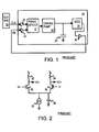
- FIG. 1 shows a zero-delay buffer that requires precise delay matching.
- Zero-delay buffer chip 10 may be integrated with a larger system or may be sold as a stand-alone zero-delay chip.
- Clock source 18 generates a reference clock CLK that is input to chip 10 .
- This reference clock passes through input buffer 22 and is compared in phase to a feedback clock FB that passes through a similar input buffer 24 .
- Phase comparator 12 compares the phases of CLK and FB and activates charge pump 14 to charge or discharge filter capacitor 20 .
- voltage-controlled oscillator VCO 16 senses the capacitor voltage and adjusts the output frequency of an output clock that is buffered by output buffer 26 .
- the FB clock output by buffer 26 can drive other logic directly, or additional internal or external buffering can generate other clocks.
- Many PLL's can be included in parallel to separately drive and adjust parallel clock lines that are synchronized to each other and to the reference clock.
- Input buffers 22 , 24 must to have closely matched delays. Otherwise a phase error is introduced that can cause VCO 16 to output the wrong frequency.
- the physical design of input buffers 22 , 24 can be closely matched to avoid skews.
- clock source 18 may have a different driver than output buffer 26 , and may drive less current or may drive signal edges more slowly.
- the metal traces for CLK and FB may also differ.
- the FB clock trace may be much shorter than the reference clock CLK trace.
- Input buffers that can adapt for such external mis-matches are desirable.
- FIG. 2 shows a prior-art differential input buffer.
- Inputs signals V+, V ⁇ are applied to the gates of n-channel differential transistors 36 , 38 , respectively.
- Resistor loads 32 , 34 supply matched currents to transistors 36 , 38 , and these currents are combined at current sink 30 .
- Differential outputs VO ⁇ , VO+ are taken from the drains of transistors 36 , 38 , respectively.
- Such a differential buffer is delay-independent of common-mode level within a certain range.
- the differential transistors tend to linearize I/Vin, for a range of about 2 ⁇ V, where ⁇ V is the gate bias of transistors 36 , 38 , or Vgs ⁇ Vt, where Vgs is the average gate-to-source voltage and Vt is the n-channel transistor threshold voltage.
- ⁇ V is the gate bias of transistors 36 , 38
- Vgs ⁇ Vt Vgs is the average gate-to-source voltage
- Vt is the n-channel transistor threshold voltage.
- non-linear delays occur beyond this 2 ⁇ V range.
- tail capacitor 28 One source of delay variation is the parasitic tail capacitance represented by tail capacitor 28 .
- tail capacitor 28 When inputs V+, V ⁇ differ by more than 2 ⁇ V, one of differential transistors 36 , 38 may turn off completely. All of the tail current then flows through the other differential transistor. As the input voltage V+ or V ⁇ rises even more, the tail voltage also rises rather than remaining constant. The rising tail voltage charges tail capacitor 28 , requiring some of the current.
- FIG. 1 shows a zero-delay buffer that requires precise delay matching.
- FIG. 2 shows a prior-art differential input buffer.
- FIG. 3 is a block diagram of a clamped differential input buffer with a well-controlled bias circuit.
- FIG. 4 is a schematic of one embodiment of the differential input clamp.
- FIG. 5 is a schematic of an embodiment of the first differential stage.
- FIG. 6 is a diagram highlighting principles of a current-mirroring bias-voltage generator.
- FIG. 7 highlights substituting a resistor that sets a voltage due to current injected and extracted from the circuit at the resistor terminals.
- FIG. 8 is a diagram of a bias current generator.
- FIG. 9 shows an alternate embodiment of a voltage-to-current reference.
- FIG. 10 is a plot of delay sensitivity to input characteristics.
- the present invention relates to an improvement in differential buffers.
- the following description is presented to enable one of ordinary skill in the art to make and use the invention as provided in the context of a particular application and its requirements.
- Various modifications to the preferred embodiment will be apparent to those with skill in the art, and the general principles defined herein may be applied to other embodiments. Therefore, the present invention is not intended to be limited to the particular embodiments shown and described, but is to be accorded the widest scope consistent with the principles and novel features herein disclosed.
- input buffers can better match in delay when input voltages do not have wide swings.
- An input clamp on the differential inputs limits the voltages of the differential inputs before they are applied to a differential amplifier. This input clamp prevents the clamped differential inputs from differing by more than the unclamped input, preventing non-linear effects caused by charging and discharging of tail capacitance.
- FIG. 3 is a block diagram of a clamped differential input buffer with a well-controlled bias circuit.
- Input clamp 300 receives differential inputs V+, V ⁇ . When V+ or V ⁇ are above a limiting voltage level, input clamp 300 reduces the input voltage to the limiting voltage. Otherwise the inputs are level-shifted and output as clamped differential inputs VC+, VC ⁇ .
- First differential stage 302 receives the clamped differential inputs VC+, VC ⁇ .
- the clamped differential inputs are limited in voltage.
- the voltage differential is allowed to be slightly more than 2 ⁇ V, but is clamped at less than the full input swing, allowing first differential stage 302 to operate in the linear range. This prevents large delay mis-matches caused by charging and discharging the tail capacitor.
- First differential stage 302 generates differential outputs VO+, VO ⁇ which may be further amplified by second differential stage 302 ′, which generates final outputs VO 2 +, VO 2 ⁇ .
- the second differential stage is optional but desirable.
- bias voltage generator 306 which mirrors a current generated by voltage-to-current reference 304 .
- FIG. 4 is a schematic of one embodiment of the differential input clamp.
- Input clamp 300 receives differential inputs V+, V ⁇ which are applied to the gates of n-channel follower transistors 62 , 64 , respectively.
- follower transistors 62 , 64 act as source-followers, shifting the input voltages V+, V ⁇ lower by at least a threshold.
- Resistors 70 , 72 sink current from follower transistors 62 , 64 respectively.
- n-channel follower transistor 62 is applied to the gate of p-channel clamp transistor 68 , which has its drain grounded.
- the source of p-channel clamp transistor 68 is the clamped output VC+.
- Resistors 76 , 77 form a voltage divider to clamped output VC+ that set the clamped voltage level when p-channel clamp transistor 68 is shut off.
- n-channel follower transistor 64 is applied to the gate of p-channel clamp transistor 66 , which has its drain grounded.
- the source of p-channel clamp transistor 66 is the clamped output VC ⁇ .
- Resistors 74 , 75 form a voltage divider to clamped output VC ⁇ that set the clamped voltage level when p-channel clamp transistor 66 is shut off.
- n-channel follower transistor 62 turns off, and resistor 70 drives the gate of p-channel clamp transistor 68 to ground, turning it on. Since the drain and gate of p-channel clamp transistor 68 are grounded, it is in the saturated region of operation and its source is clamped to one threshold above its gate, or
- the lower clamped voltage of VC+ is about
- n-channel follower transistor 62 When V+ is above the clamped voltage input level, n-channel follower transistor 62 is on strongly, pulling the gate of p-channel clamp transistor 68 high. When a sufficiently high voltage is applied, p-channel clamp transistor 68 turns off. Then resistors 76 , 77 form a voltage divider that determines the upper clamped voltage output on VC+.
- clamped voltage input levels on inputs V+, V ⁇ can be different from the clamped voltages on clamped outputs VC+, VC ⁇ .
- a benefit of this embodiment of input clamp 300 is that the maximum clamped output voltages can be set by sizing the voltage-divider resistors while the minimum clamped output voltage is set by the p-channel threshold
- FIG. 5 is a schematic of an embodiment of the first differential stage.
- First differential stage 302 receives clamped differential inputs VC+, VC ⁇ from input clamp 300 that are limited in voltage swing. This limited input-voltage swing limits charging and discharging of tail capacitances such as tail capacitor 54 , reducing non-linearities.
- Clamped differential input VC+ is applied to the gate of n-channel differential transistor 42
- input VC ⁇ is applied to the gate of n-channel differential transistor 44 .
- both differential transistors 42 , 44 connect to the same current sink
- separate current sinks 50 , 52 connect to transistors 42 , 44 , respectively.
- Current sink 50 receives currents from differential transistor 42 and n-channel common-mode transistor 46 .
- current sink 52 receives currents from differential transistor 44 and n-channel common-mode transistor 48 .
- Common-mode transistors 46 , 48 are driven by a common-mode or mid-point voltage VMID, which is between VC+ and VC ⁇ .
- VMID can be generated dynamically by a 50%—50% voltage divider between VC+ and VC ⁇ , or it can be generated statically at a pre-determined middle voltage such as 2.0 volts or 1.2 volts.
- VMID is generated from the midpoint of two equal-valued resistors in series between the differential inputs.
- VMID can be isolated further by inserting a capacitor between the resistor midpoints and the use of VMID in the circuit.
- VMID follows the common-mode input. The center of the clamped differential input is filtered and responds slowly to changes in input common-mode level.
- Load current through resistor 59 is split into parallel branches by resistors 56 , 58 , which connect to the drains of common-mode transistors 46 , 48 , respectively.
- Itail normal DC bias current
- Itail When the slew current exceeds the normal DC bias current Itail, most or all of the extra current dumps into Vdd through transistor 42 or 44 , whose drain connects to the Vdd supply. Thus normal operation is relatively undisturbed.
- An n-type source follower increases Vgs on rising edges to drive a capacitive load. On falling edges, Vgs can only be reduced somewhat, and then the slew is limited by the pulldown bias current, Itail.
- transistors 46 , 48 With a fixed gate bias (VMID) connected to the output load. Since transistors 46 , 48 have a fixed input voltage VMID, they cannot experience delay variations due to gate input slew.
- First differential stage 302 is non-inverting. It can be made to invert by swapping VO+ and VO ⁇ .
- tail capacitor 54 which is not a real capacitor but instead represents the sum of all parasitic and other capacitances on the tail node.
- a second differential stage can be constructed in a similar manner, or a different circuit may be used.
- a differential-to-single-ended converter may also be included.
- Current sinks 50 , 52 can each be implemented as an n-channel transistor with its source grounded and having a gate driven by a bias voltage.
- the bias voltage can be generated by a simple bias generator such as a voltage-divider network, or a more complex bias-voltage generator can be used such as described below. Since Vgs varies with temperature and according to other variables, the current source must compensate.
- the purpose of the bias current is to cause the input differential pair to have a fixed and controlled linear input range 2 ⁇ V. In this case the 2 ⁇ V is derived from the most convenient source, Vdd. Any reference, internal or external, could be used instead. Once this is achieved all other results may be obtained by referring to this controlled 2 ⁇ V.
- FIG. 6 is a diagram highlighting principles of a current-mirroring bias-voltage generator.
- the bias voltage to the tail transistors implementing current sinks 50 , 52 can be taken from the gate voltage of transistor 86 . Vgs 2 .
- the gate and drain of p-channel mirror transistor 84 are connected together and to the gate of p-channel mirror transistor 82 .
- the current I 2 through p-channel mirror transistor 84 is four times the current I 1 through p-channel mirror transistor 82 , since transistor 86 has 4 times the W/L ratio of transistor 84 .
- other current-scaling ratios can be substituted.
- Vgs 2 ⁇ Vt 2( Vgs 1 ⁇ Vt ).
- Vgs 2 2 *Vgs 1 ⁇ Vt
- Vgs 1 + V 2 *Vgs 1 ⁇ Vt
- V Vgs 1 ⁇ Vt.
- Voltage V can be produced by substituting a resistor and driving a same current into and out of the resistor.
- FIG. 7 highlights substituting a resistor that sets a voltage due to current injected and extracted from the circuit at the resistor terminals. The voltage source is removed and resistor 94 is inserted between the drains of transistors 82 , 88 (node N 1 ) and the gate of transistor 86 . Resistor 94 creates a voltage to set ⁇ V. This voltage is a floating voltage source, one that is not referred to the power supply or to ground.
- the floating voltage source derives a voltage-to-current current from a reference voltage across a reference resistor (not shown). This current forms a precise voltage across biasing resistor 94 by current and resistance ratios from the reference resistor.
- the circuit works with any other form of floating voltage source. This particular one is well suited to low-voltage application.
- a bias current IB 1 is injected into one terminal of resistor 94 by current bias source 90 . This same current IB 1 is removed from the other terminal of resistor 94 by bias current sink 92 . Since the same current IB 1 is injected and removed from the circuit, no net current is added to node N 1 by resistor 94 .
- This gate voltage Vgs 2 is also the bias voltage for the current sinks 50 , 52 of the first differential stage 302 . Setting bias current IB 1 through resistor 94 thus sets the tail current sinks.
- FIG. 8 is a diagram of a bias current generator.
- Bias current generator 306 generates the tail voltage bias VTAIL to current sinks 50 , 52 .
- VTAIL is set by the gate voltage of n-channel transistor 86 , which sinks current I 2 set by mirror transistor 84 .
- Mirror transistor 82 and n-channel transistor 88 are connected to one terminal of bias-setting resistor 94 while the gate voltage VTAIL of transistor 86 is the other terminal of resistor 94 .
- Current injector 120 generates and removes bias current IB 1 .
- Bias current IB 1 is injected into resistor 94 by p-channel transistor 114 .
- the same bias current IB 1 is removed from the other terminal of resistor 94 by n-channel transistor 112 .
- transistors 114 , 112 match because the gate of p-channel transistor 114 is the same node as the gate of p-channel transistor 108 , and the gate of n-channel transistor 112 is the same node as n-channel transistor 110 . Since transistors 108 , 110 are connected together and must pass the same amount of current, the p-channel and n-channel currents must match.
- the IB 1 current through transistors 108 , 110 is mirrored to injected current IB 1 from p-channel transistor 114 and removed current IB 1 from n-channel transistor 112 .
- the gate and drain of n-channel transistor 110 are connected together and to the gate of n-channel transistor 112 .
- the upper gate voltage to p-channel transistors 108 , 114 is set by p-channel transistor 102 , which has its gate and drain connected together. Current through p-channel transistor 102 is set by voltage-to-current reference 304 .
- a bias voltage VB is applied to one input of comparator 100 , while the other input is feedback NFB from the source of n-channel transistor 104 .
- Comparator 100 drives the gate of n-channel transistor 104 to adjust current flow so that the source of n-channel transistor 104 , NFB, is the same voltage as VB.
- Current from n-channel transistor 104 flowing through resistor 106 produces a voltage drop NFB that is matched to VB.
- V VB*R 1 / R 2 .
- FIG. 9 shows an alternate embodiment of an amplifier-based voltage-to-current reference.
- Voltage VBIAS is generated by voltage source 154 and raises the source voltage of n-channel transistor 152 .
- the gate and drain of n-channel transistor 152 are connected together and to the gate of n-channel transistor 162 in the other leg.
- p-channel transistor 150 Current is sourced by p-channel transistor 150 to the drain of n-channel transistors 52 , and by p-channel transistor 160 to the drain of n-channel transistor 162 .
- the gate and drain of p-channel transistor 160 are connected together to set the gate voltage of p-channel transistors 150 , 160 .
- Resistor 156 receives current from the source of n-channel transistor 162 and sets VR.
- Voltage-to-current reference 304 can generate the p-channel gate voltage to p-channel transistors 108 , 114 of FIG. 8 .
- P-channel transistor 102 in FIG. 8 is the same as p-channel transistor 160 of FIG. 9 .
- FIG. 10 is a plot of delay sensitivity to input characteristics.
- the delay through a prior-art differential buffer such as shown in FIG. 2 is plotted as lines 202 .
- the vertical axis is delay while the horizontal axis is the common-mode offset.
- the four lines in lines 202 are for different input amplitudes, or the maximum difference of V+ and V ⁇ .
- the amplitude difference is stepped from 0.6 to 1.8 volts in four steps.
- the clamped buffer has a minimum delay of 865 ps and a maximum delay of 880 ps, for a difference in delay of only 15 ps.
- the delay range is reduced from 40 ps (840-800 ps) for the standard buffer to 3 ps (860-857 ps) for the new clamped buffer.
- delay range and sensitivity to amplitude is reduced by more than a factor of 10.
- matched input buffers can occur on many other kinds of circuits besides zero-delay buffers.
- High-speed data busses may benefit from better-matches input buffers, address and control signals that match more closely may allow a system to be run at a higher rate, and communication lines may benefit from better signal matching.
- Output buffers or general drivers could benefit from the invention, because their delays could match. Data and other communication receivers would benefit also, because different inputs would have equal delays.
- bias-voltage generators clamps, and differential stages can be substituted.
- amplifiers with active loads and clamps could be used instead of resistors.
- a fixed current could be used for the bias generator.
- a differential clamp of the passive or active variety could be used instead of one referred to the supplies.
- Resistor loads could be added above the differential transistors in the first differential stage. Rather than use resistor loads, transistor loads can be used, and controlled bias voltages can drive gates of these load transistors.
Landscapes
- Physics & Mathematics (AREA)
- Nonlinear Science (AREA)
- Amplifiers (AREA)
Abstract
Description
Claims (19)
Priority Applications (1)
| Application Number | Priority Date | Filing Date | Title |
|---|---|---|---|
| US10/249,414 US6801080B1 (en) | 2003-04-07 | 2003-04-07 | CMOS differential input buffer with source-follower input clamps |
Applications Claiming Priority (1)
| Application Number | Priority Date | Filing Date | Title |
|---|---|---|---|
| US10/249,414 US6801080B1 (en) | 2003-04-07 | 2003-04-07 | CMOS differential input buffer with source-follower input clamps |
Publications (1)
| Publication Number | Publication Date |
|---|---|
| US6801080B1 true US6801080B1 (en) | 2004-10-05 |
Family
ID=33029560
Family Applications (1)
| Application Number | Title | Priority Date | Filing Date |
|---|---|---|---|
| US10/249,414 Expired - Fee Related US6801080B1 (en) | 2003-04-07 | 2003-04-07 | CMOS differential input buffer with source-follower input clamps |
Country Status (1)
| Country | Link |
|---|---|
| US (1) | US6801080B1 (en) |
Cited By (16)
| Publication number | Priority date | Publication date | Assignee | Title |
|---|---|---|---|---|
| US20040059845A1 (en) * | 2002-09-25 | 2004-03-25 | Samsung Electronics Co., Ltd. | Simultaneous bidirectional input/output circuit |
| US20050134494A1 (en) * | 2003-12-09 | 2005-06-23 | Matsushita Electric Industrial Co., Ltd. | Inverter control device and inverter control method |
| US7034615B2 (en) * | 2003-01-20 | 2006-04-25 | Lg Electronics Inc. | CMOS operational amplifier |
| US7142005B1 (en) * | 2003-11-26 | 2006-11-28 | Xilinx, Inc. | Method and apparatus for a reference clock buffer system |
| US20080036516A1 (en) * | 2006-08-09 | 2008-02-14 | Atmel Corporation | Apparatus and method for charge pump slew rate control |
| US7355450B1 (en) | 2005-05-27 | 2008-04-08 | Altera Corporation | Differential input buffers for low power supply |
| CN101534187A (en) * | 2008-03-12 | 2009-09-16 | 索尼株式会社 | Communication system, receiver and reception method |
| US20100289581A1 (en) * | 2009-05-15 | 2010-11-18 | Mi Hye Kim | Differential amplifying device |
| US20100308884A1 (en) * | 2009-06-09 | 2010-12-09 | Hynix Semiconductor Inc. | Clock receiver in semiconductor integrated circuit and method of controlling the same |
| US20130049864A1 (en) * | 2011-08-29 | 2013-02-28 | Natsuki IKEHATA | Semiconductor integrated circuit device |
| US20160006395A1 (en) * | 2014-07-07 | 2016-01-07 | Electronics And Telecommunications Research Institute | Buffer amplifier and trans-impedance amplifier including the same |
| US20180226960A1 (en) * | 2017-02-07 | 2018-08-09 | Kabushiki Kaisha Toshiba | Comparator |
| US10622980B1 (en) | 2018-11-09 | 2020-04-14 | Analog Devices, Inc. | Apparatus and methods for setting and clamping a node voltage |
| US10965215B2 (en) * | 2019-08-15 | 2021-03-30 | Microchip Technology Incorporated | Constant on-time buck converter with calibrated ripple injection having improved light load transient response and reduced output capacitor size |
| CN115459777A (en) * | 2022-09-23 | 2022-12-09 | 中科芯集成电路有限公司 | Biasing circuit suitable for differential current steering DAC |
| WO2024094784A1 (en) * | 2022-11-03 | 2024-05-10 | Analog Devices International Unlimited Company | Common mode voltage clamp for multidrop networks |
Citations (26)
| Publication number | Priority date | Publication date | Assignee | Title |
|---|---|---|---|---|
| US3679989A (en) | 1970-11-16 | 1972-07-25 | Rca Corp | Clamp circuit for preventing saturation of operational amplifier |
| US4206418A (en) | 1978-07-03 | 1980-06-03 | Rca Corporation | Circuit for limiting voltage differential in differential amplifiers |
| US4808944A (en) * | 1987-11-23 | 1989-02-28 | Triquint Semiconductor, Inc. | High accuracy differential output stage |
| US4935649A (en) | 1988-07-11 | 1990-06-19 | Cypress Semiconductor Corporation | Clamped sense amplifier |
| US4945262A (en) | 1989-01-26 | 1990-07-31 | Harris Corporation | Voltage limiter apparatus with inherent level shifting employing MOSFETs |
| US5196744A (en) | 1990-07-23 | 1993-03-23 | Bull, S.A. | Peak clipping circuit |
| US5256917A (en) | 1992-04-03 | 1993-10-26 | Motorola, Inc. | ECL logic gate with voltage protection |
| US5315179A (en) * | 1992-09-28 | 1994-05-24 | Motorola, Inc. | BICMOS level converter circuit |
| US5570042A (en) | 1995-01-03 | 1996-10-29 | Sgs-Thomson Microelectronics, Inc. | PECL input buffer |
| US5585743A (en) * | 1992-10-14 | 1996-12-17 | Fujitsu Limited | ECL-CMOS level conversion circuit |
| US5701102A (en) * | 1995-11-29 | 1997-12-23 | National Semiconductor Corporation | High-speed transmission line receiver with wide range of common mode compensation |
| US5869985A (en) * | 1997-02-07 | 1999-02-09 | Eic Enterprises Corporation | Low voltage input buffer |
| US5898341A (en) * | 1995-04-10 | 1999-04-27 | Fujitsu Limited | Differential amplification circuit and method of noise removal |
| US5942921A (en) | 1997-12-19 | 1999-08-24 | Advanced Micro Devices, Inc. | Differential comparator with an extended input range |
| US5973561A (en) * | 1997-06-03 | 1999-10-26 | Texas Instruments Incorporated | Differential clamp for amplifier circuits |
| US5990708A (en) | 1997-02-03 | 1999-11-23 | Texas Instruments Incorporated | Differential input buffer using local reference voltage and method of construction |
| US6094093A (en) * | 1997-01-22 | 2000-07-25 | Lucent Technologies Inc. | Low-voltage input buffer |
| US6107856A (en) | 1997-12-30 | 2000-08-22 | Lsi Logic Corporation | Dual output comparator for operating over a wide common mode range |
| US6114872A (en) | 1996-05-31 | 2000-09-05 | Nippon Steel Corporation | Differential input circuit |
| US6265926B1 (en) | 1998-05-27 | 2001-07-24 | Altera Corporation | Programmable PCI overvoltage input clamp |
| US6456137B1 (en) * | 1999-11-24 | 2002-09-24 | Nec Corporation | Semiconductor circuit, delay adjustment method therefor and layout method therefor |
| US6496070B2 (en) * | 2000-06-12 | 2002-12-17 | Fujitsu Quantum Devices Limited | Buffer circuit comprising load, follower transistor and current source connected in series |
| US6525607B1 (en) * | 2000-09-27 | 2003-02-25 | Intel Corporation | High-voltage differential input receiver |
| US6528978B2 (en) * | 2001-03-08 | 2003-03-04 | Samsung Electronics Co., Ltd. | Reference voltage generator |
| US6552611B2 (en) * | 2000-03-27 | 2003-04-22 | Kabushiki Kaisha Toshiba | Differential amplifier and filter circuit using the same |
| US6583668B1 (en) * | 2001-05-11 | 2003-06-24 | Euvis, Inc. | Wideband variable gain amplifier with low power supply voltage |
-
2003
- 2003-04-07 US US10/249,414 patent/US6801080B1/en not_active Expired - Fee Related
Patent Citations (27)
| Publication number | Priority date | Publication date | Assignee | Title |
|---|---|---|---|---|
| US3679989A (en) | 1970-11-16 | 1972-07-25 | Rca Corp | Clamp circuit for preventing saturation of operational amplifier |
| US4206418A (en) | 1978-07-03 | 1980-06-03 | Rca Corporation | Circuit for limiting voltage differential in differential amplifiers |
| US4808944A (en) * | 1987-11-23 | 1989-02-28 | Triquint Semiconductor, Inc. | High accuracy differential output stage |
| US4935649A (en) | 1988-07-11 | 1990-06-19 | Cypress Semiconductor Corporation | Clamped sense amplifier |
| US4945262A (en) | 1989-01-26 | 1990-07-31 | Harris Corporation | Voltage limiter apparatus with inherent level shifting employing MOSFETs |
| US5196744A (en) | 1990-07-23 | 1993-03-23 | Bull, S.A. | Peak clipping circuit |
| US5256917A (en) | 1992-04-03 | 1993-10-26 | Motorola, Inc. | ECL logic gate with voltage protection |
| US5315179A (en) * | 1992-09-28 | 1994-05-24 | Motorola, Inc. | BICMOS level converter circuit |
| US5585743A (en) * | 1992-10-14 | 1996-12-17 | Fujitsu Limited | ECL-CMOS level conversion circuit |
| US5570042A (en) | 1995-01-03 | 1996-10-29 | Sgs-Thomson Microelectronics, Inc. | PECL input buffer |
| US5570042B1 (en) | 1995-01-03 | 2000-10-17 | Sgs Thomson Micro Electronics | Pecl input buffer |
| US5898341A (en) * | 1995-04-10 | 1999-04-27 | Fujitsu Limited | Differential amplification circuit and method of noise removal |
| US5701102A (en) * | 1995-11-29 | 1997-12-23 | National Semiconductor Corporation | High-speed transmission line receiver with wide range of common mode compensation |
| US6114872A (en) | 1996-05-31 | 2000-09-05 | Nippon Steel Corporation | Differential input circuit |
| US6094093A (en) * | 1997-01-22 | 2000-07-25 | Lucent Technologies Inc. | Low-voltage input buffer |
| US5990708A (en) | 1997-02-03 | 1999-11-23 | Texas Instruments Incorporated | Differential input buffer using local reference voltage and method of construction |
| US5869985A (en) * | 1997-02-07 | 1999-02-09 | Eic Enterprises Corporation | Low voltage input buffer |
| US5973561A (en) * | 1997-06-03 | 1999-10-26 | Texas Instruments Incorporated | Differential clamp for amplifier circuits |
| US5942921A (en) | 1997-12-19 | 1999-08-24 | Advanced Micro Devices, Inc. | Differential comparator with an extended input range |
| US6107856A (en) | 1997-12-30 | 2000-08-22 | Lsi Logic Corporation | Dual output comparator for operating over a wide common mode range |
| US6265926B1 (en) | 1998-05-27 | 2001-07-24 | Altera Corporation | Programmable PCI overvoltage input clamp |
| US6456137B1 (en) * | 1999-11-24 | 2002-09-24 | Nec Corporation | Semiconductor circuit, delay adjustment method therefor and layout method therefor |
| US6552611B2 (en) * | 2000-03-27 | 2003-04-22 | Kabushiki Kaisha Toshiba | Differential amplifier and filter circuit using the same |
| US6496070B2 (en) * | 2000-06-12 | 2002-12-17 | Fujitsu Quantum Devices Limited | Buffer circuit comprising load, follower transistor and current source connected in series |
| US6525607B1 (en) * | 2000-09-27 | 2003-02-25 | Intel Corporation | High-voltage differential input receiver |
| US6528978B2 (en) * | 2001-03-08 | 2003-03-04 | Samsung Electronics Co., Ltd. | Reference voltage generator |
| US6583668B1 (en) * | 2001-05-11 | 2003-06-24 | Euvis, Inc. | Wideband variable gain amplifier with low power supply voltage |
Cited By (30)
| Publication number | Priority date | Publication date | Assignee | Title |
|---|---|---|---|---|
| US20040059845A1 (en) * | 2002-09-25 | 2004-03-25 | Samsung Electronics Co., Ltd. | Simultaneous bidirectional input/output circuit |
| US7102545B2 (en) * | 2002-09-25 | 2006-09-05 | Samsung Electronics Co., Ltd. | Simultaneous bidirectional input/output circuit |
| US7034615B2 (en) * | 2003-01-20 | 2006-04-25 | Lg Electronics Inc. | CMOS operational amplifier |
| US7142005B1 (en) * | 2003-11-26 | 2006-11-28 | Xilinx, Inc. | Method and apparatus for a reference clock buffer system |
| US20050134494A1 (en) * | 2003-12-09 | 2005-06-23 | Matsushita Electric Industrial Co., Ltd. | Inverter control device and inverter control method |
| US7355450B1 (en) | 2005-05-27 | 2008-04-08 | Altera Corporation | Differential input buffers for low power supply |
| US7365585B2 (en) | 2006-08-09 | 2008-04-29 | Atmel Corporation | Apparatus and method for charge pump slew rate control |
| US20080036516A1 (en) * | 2006-08-09 | 2008-02-14 | Atmel Corporation | Apparatus and method for charge pump slew rate control |
| US8467490B2 (en) * | 2008-03-12 | 2013-06-18 | Sony Corporation | Communication system, receiver and reception method |
| CN101534187A (en) * | 2008-03-12 | 2009-09-16 | 索尼株式会社 | Communication system, receiver and reception method |
| US20090232250A1 (en) * | 2008-03-12 | 2009-09-17 | Takaaki Yamada | Communication system, receiver and reception method |
| US20100289581A1 (en) * | 2009-05-15 | 2010-11-18 | Mi Hye Kim | Differential amplifying device |
| US7999611B2 (en) | 2009-05-15 | 2011-08-16 | Hynix Semiconductor Inc. | Differential amplifying device |
| US20100308884A1 (en) * | 2009-06-09 | 2010-12-09 | Hynix Semiconductor Inc. | Clock receiver in semiconductor integrated circuit and method of controlling the same |
| US8350604B2 (en) | 2009-06-09 | 2013-01-08 | Hynix Semiconductor Inc. | Clock receiver in semiconductor integrated circuit and method of controlling the same |
| US20130049864A1 (en) * | 2011-08-29 | 2013-02-28 | Natsuki IKEHATA | Semiconductor integrated circuit device |
| US8803610B2 (en) * | 2011-08-29 | 2014-08-12 | Renesas Electronics Corporation | Semiconductor integrated circuit device |
| US9214217B2 (en) | 2011-08-29 | 2015-12-15 | Renesas Electronics Corporation | Semiconductor integrated circuit device |
| TWI612529B (en) * | 2011-08-29 | 2018-01-21 | 瑞薩電子股份有限公司 | Semiconductor integrated circuit device |
| US20160006395A1 (en) * | 2014-07-07 | 2016-01-07 | Electronics And Telecommunications Research Institute | Buffer amplifier and trans-impedance amplifier including the same |
| KR20160005431A (en) * | 2014-07-07 | 2016-01-15 | 한국전자통신연구원 | Buffer amplifier and trans impedance amplifier including buffer amplifier |
| US9425743B2 (en) * | 2014-07-07 | 2016-08-23 | Electronics And Telecommunications Research Instit | Buffer amplifier and trans-impedance amplifier including the same |
| US20180226960A1 (en) * | 2017-02-07 | 2018-08-09 | Kabushiki Kaisha Toshiba | Comparator |
| US10601411B2 (en) * | 2017-02-07 | 2020-03-24 | Kabushiki Kaisha Toshiba | Comparator |
| US10622980B1 (en) | 2018-11-09 | 2020-04-14 | Analog Devices, Inc. | Apparatus and methods for setting and clamping a node voltage |
| US10965215B2 (en) * | 2019-08-15 | 2021-03-30 | Microchip Technology Incorporated | Constant on-time buck converter with calibrated ripple injection having improved light load transient response and reduced output capacitor size |
| CN115459777A (en) * | 2022-09-23 | 2022-12-09 | 中科芯集成电路有限公司 | Biasing circuit suitable for differential current steering DAC |
| CN115459777B (en) * | 2022-09-23 | 2025-11-28 | 中科芯集成电路有限公司 | Bias circuit suitable for differential current rudder DAC |
| WO2024094784A1 (en) * | 2022-11-03 | 2024-05-10 | Analog Devices International Unlimited Company | Common mode voltage clamp for multidrop networks |
| US12476454B2 (en) | 2022-11-03 | 2025-11-18 | Analog Devices International Unlimited Company | Common mode voltage clamp for multidrop networks |
Similar Documents
| Publication | Publication Date | Title |
|---|---|---|
| US6801080B1 (en) | CMOS differential input buffer with source-follower input clamps | |
| USRE49018E1 (en) | Charge pump for PLL/DLL | |
| US6316987B1 (en) | Low-power low-jitter variable delay timing circuit | |
| US5945855A (en) | High speed phase lock loop having high precision charge pump with error cancellation | |
| US6320435B1 (en) | PLL circuit which can reduce phase offset without increase in operation voltage | |
| US6583657B1 (en) | Single-edge clock adjustment circuits for PLL-compatible, dynamic duty-cycle correction circuits | |
| US6643790B1 (en) | Duty cycle correction circuit with frequency-dependent bias generator | |
| US7535272B1 (en) | Zero-delay buffer with common-mode equalizer for input and feedback differential clocks into a phase-locked loop (PLL) | |
| US7977985B2 (en) | Bias generator providing for low power, self-biased delay element and delay line | |
| US7965118B2 (en) | Method and apparatus for achieving 50% duty cycle on the output VCO of a phased locked loop | |
| US7812652B2 (en) | Locked loops, bias generators, charge pumps and methods for generating control voltages | |
| JP3109560B2 (en) | Semiconductor integrated circuit using variation compensation technology | |
| CN107612529A (en) | A kind of clock duty cycle auto-adjusting circuit | |
| US20050122146A1 (en) | Precise slew rate control line driver | |
| US20080186075A1 (en) | Level shifter of semiconductor device and method for controlling duty ratio in the device | |
| US9548727B2 (en) | Oscillator circuit | |
| US6384620B1 (en) | Signal deciding apparatus | |
| US7453313B2 (en) | Charge pumping circuit | |
| US6806741B2 (en) | Phase comparator capable of performing stable phase comparison for high frequency band | |
| US7705642B2 (en) | Simplified bias circuitry for differential buffer stage with symmetric loads | |
| US9621022B1 (en) | Method and apparatus for generating complementary signals | |
| JPH04154314A (en) | Output circuit | |
| Li et al. | A supply noise compensation circuit for clock buffers to reduce timing jitter |
Legal Events
| Date | Code | Title | Description |
|---|---|---|---|
| AS | Assignment |
Owner name: PERICOM SEMICONDUCTOR CORP., CALIFORNIA Free format text: ASSIGNMENT OF ASSIGNORS INTEREST;ASSIGNOR:ARCUS, CHRISTOPHER G.;REEL/FRAME:013650/0683 Effective date: 20030502 |
|
| FEPP | Fee payment procedure |
Free format text: PAT HOLDER NO LONGER CLAIMS SMALL ENTITY STATUS, ENTITY STATUS SET TO UNDISCOUNTED (ORIGINAL EVENT CODE: STOL); ENTITY STATUS OF PATENT OWNER: LARGE ENTITY |
|
| FPAY | Fee payment |
Year of fee payment: 4 |
|
| FPAY | Fee payment |
Year of fee payment: 8 |
|
| AS | Assignment |
Owner name: BANK OF AMERICA, N.A., AS ADMINISTRATIVE AGENT, TE Free format text: SECURITY INTEREST;ASSIGNOR:PERICOM SEMICONDUCTOR CORPORATION, AS GRANTOR;REEL/FRAME:037255/0122 Effective date: 20151209 |
|
| REMI | Maintenance fee reminder mailed | ||
| LAPS | Lapse for failure to pay maintenance fees | ||
| STCH | Information on status: patent discontinuation |
Free format text: PATENT EXPIRED DUE TO NONPAYMENT OF MAINTENANCE FEES UNDER 37 CFR 1.362 |
|
| STCH | Information on status: patent discontinuation |
Free format text: PATENT EXPIRED DUE TO NONPAYMENT OF MAINTENANCE FEES UNDER 37 CFR 1.362 |
|
| FP | Lapsed due to failure to pay maintenance fee |
Effective date: 20161005 |
|
| AS | Assignment |
Owner name: DIODES INCORPORATED, TEXAS Free format text: ASSIGNMENT OF ASSIGNORS INTEREST;ASSIGNOR:PERICOM SEMICONDUCTOR CORPORATION;REEL/FRAME:044975/0554 Effective date: 20171222 |
|
| AS | Assignment |
Owner name: BANK OF AMERICA, N.A., AS ADMIN. AGENT, NORTH CAROLINA Free format text: SECURITY AGREEMENT;ASSIGNOR:DIODES INCORPORATED;REEL/FRAME:045195/0446 Effective date: 20180122 Owner name: BANK OF AMERICA, N.A., AS ADMIN. AGENT, NORTH CARO Free format text: SECURITY AGREEMENT;ASSIGNOR:DIODES INCORPORATED;REEL/FRAME:045195/0446 Effective date: 20180122 |