US6800404B2 - Method for producing a self-supporting electron-optical transparent structure, and structure produced in accordance with the method - Google Patents

Method for producing a self-supporting electron-optical transparent structure, and structure produced in accordance with the method Download PDF

Info

Publication number
US6800404B2
US6800404B2 US10/209,186 US20918602A US6800404B2 US 6800404 B2 US6800404 B2 US 6800404B2 US 20918602 A US20918602 A US 20918602A US 6800404 B2 US6800404 B2 US 6800404B2
Authority
US
United States
Prior art keywords
layer
accordance
strips
electron
optical transparent
Prior art date
Legal status (The legal status is an assumption and is not a legal conclusion. Google has not performed a legal analysis and makes no representation as to the accuracy of the status listed.)
Expired - Fee Related, expires
Application number
US10/209,186
Other versions
US20030036022A1 (en
Inventor
Peter Speckbacher
Georg Flatscher
Michael Allgäuer
Erich Bayer
Anton Sailer
Martin Ullrich
Current Assignee (The listed assignees may be inaccurate. Google has not performed a legal analysis and makes no representation or warranty as to the accuracy of the list.)
Dr Johannes Heidenhain GmbH
Original Assignee
Dr Johannes Heidenhain GmbH
Priority date (The priority date is an assumption and is not a legal conclusion. Google has not performed a legal analysis and makes no representation as to the accuracy of the date listed.)
Filing date
Publication date
Application filed by Dr Johannes Heidenhain GmbH filed Critical Dr Johannes Heidenhain GmbH
Assigned to DR. JOHANNES HEIDENHAIN GMBH reassignment DR. JOHANNES HEIDENHAIN GMBH ASSIGNMENT OF ASSIGNORS INTEREST (SEE DOCUMENT FOR DETAILS). Assignors: BAYER, ERICH, ALLGAUER, MICHAEL, SAILER, ANTON, SPECKBACHER, PETER, ULLRICH, MARTIN, FLATSCHER, GEORG
Publication of US20030036022A1 publication Critical patent/US20030036022A1/en
Application granted granted Critical
Publication of US6800404B2 publication Critical patent/US6800404B2/en
Adjusted expiration legal-status Critical
Expired - Fee Related legal-status Critical Current

Links

Images

Classifications

    • GPHYSICS
    • G03PHOTOGRAPHY; CINEMATOGRAPHY; ANALOGOUS TECHNIQUES USING WAVES OTHER THAN OPTICAL WAVES; ELECTROGRAPHY; HOLOGRAPHY
    • G03FPHOTOMECHANICAL PRODUCTION OF TEXTURED OR PATTERNED SURFACES, e.g. FOR PRINTING, FOR PROCESSING OF SEMICONDUCTOR DEVICES; MATERIALS THEREFOR; ORIGINALS THEREFOR; APPARATUS SPECIALLY ADAPTED THEREFOR
    • G03F1/00Originals for photomechanical production of textured or patterned surfaces, e.g., masks, photo-masks, reticles; Mask blanks or pellicles therefor; Containers specially adapted therefor; Preparation thereof
    • G03F1/20Masks or mask blanks for imaging by charged particle beam [CPB] radiation, e.g. by electron beam; Preparation thereof
    • HELECTRICITY
    • H01ELECTRIC ELEMENTS
    • H01JELECTRIC DISCHARGE TUBES OR DISCHARGE LAMPS
    • H01J2237/00Discharge tubes exposing object to beam, e.g. for analysis treatment, etching, imaging
    • H01J2237/30Electron or ion beam tubes for processing objects
    • H01J2237/317Processing objects on a microscale
    • H01J2237/3175Lithography
    • H01J2237/31793Problems associated with lithography
    • H01J2237/31794Problems associated with lithography affecting masks

Definitions

  • the present invention relates to a method for producing a self-supporting electron-optical transparent structure, composed of strips of several layers and recesses located between the strips.
  • the present invention also relates to a structure produced in accordance with the method.
  • Electron-optical transparent structures are employed for example as absorbing structures, often also called masks, in electron-beam lithography.
  • periodically repeated patterns (“cell projection”), or patterns of variable size (“variable shaped beam”), are projected by means of these structures, which are capable of beam absorption, on substrates appropriately coated with light-sensitive materials, which in the end can be used as patterns for wafer steppers in the semiconductor industry, or as scale graduations.
  • electron beams arriving in partial areas, for example strips of the structure are absorbed by the structure, while the electron beam is spread as unimpeded as possible through recesses between the strips.
  • structures are employed which not rarely have distances of less than 500 nm between the strips, wherein the strip widths are often less than 1 ⁇ m. Moreover, the structures should not be too thin in order to achieve the necessary image quality, or the required degree of absorption, so that strip heights of 750 nm and more must be attempted.
  • a method for producing metallic foil masks is described in laid-open DE 1 521 476, wherein the foil masks are initially placed by vapor deposition on a metal matrix and thereafter are again drawn off this matrix. It is known that by the vapor-deposition process it is only possible to produce foil masks of comparatively little thickness within a reasonable amount of time. Customarily, layer thicknesses of 500 nm are not exceeded today, inter alia because of the long deposition times in the vapor-deposition process.
  • a mask includes several metal layers is disclosed in German Letters Patent DE 23 44 111.
  • a layer of precious metal is applied by galvanization to a support substrate layer. Following galvanization, the two layers are inseparably connected with each other. Because of the process, no filigreed multi-layered structures can be produced in this way, because for reasons of their being manipulable alone, the support substrate layers must already have a sufficient thickness at the start of the process.
  • An object of the present invention is based on making available a method for producing a self-supporting electron-optical transparent structure, by which it is possible in particular to produce extremely filigreed and accurate patterns.
  • the structures produced in this way differ, inter alia, by their increased fineness and the more even shape of the strip edges.
  • a method for producing a self-supporting electron-optical transparent structure that includes multi-layer strips and recesses located between the multi-layer strips.
  • the method includes applying a first layer to a second layer, presetting a pattern by exposing or irradiating the first layer and etching the pattern out of the first layer so that partial areas of the second layer are uncovered.
  • the method further includes galvanically applying layers to the uncovered partial areas of the second layer so that multi-layer strips are formed thereon and an electron-optical transparent structure is formed and removing the electron-optical transparent structure off the second layer.
  • a self-supporting electron-optical transparent structure that includes multi-layer strips and recesses located between the multi-layer strips.
  • the structure is made by a process that includes applying a first layer to a second layer, presetting a pattern by exposing or irradiating the first layer and etching the pattern out of the first layer so that partial areas of the second layer are uncovered.
  • the method further includes galvanically applying layers to the uncovered partial areas of the second layer so that multi-layer strips are formed thereon and an electron-optical transparent structure is formed and removing the electron-optical transparent structure off the second layer.
  • the present invention is based on the concept that a fine, multi-layered structure is galvanically applied between border walls to an electrically conductive auxiliary layer, and that the thin structure can be pulled, without being destroyed, off this auxiliary layer.
  • galvanic application of the layers of the structure it is relatively rapidly and easily possible to obtain layer thicknesses far exceeding 500 nm, so that high-energy electrons can be completely absorbed.
  • the advantage obtained by the present invention includes making possible the production of extremely filigreed and even self-supporting electron-optical transparent structures.
  • a two-stage etching process is used for bringing out the desired pattern, wherein an electrically conductive layer is used as the etch stop layer.
  • Plasma etching processes are employed in connection with a preferred method variation. Other dry etching or wet etching processes can also be used.
  • etching not only relates to the dissolution of materials in acids, but also to a corresponding method employing bases.
  • a galvanic process is understood to be a method wherein layer materials are applied from an ionized state. It is for example possible to electrolytically precipitate metals, such as gold or nickel, out of a preferably aqueous solution to the appropriate surface. Metal ions are discharged and deposited at the cathode. It is possible in the end to build up the desired layer thickness by adjusting the electrical current and the length of the process.
  • FIGS. 1 a to 1 k represent partial cross sections through auxiliary layers and layers of an embodiment of a multilayer structure in accordance with the following invention following various process steps of a process in accordance with the present invention
  • FIG. 2 is a view from above of the multilayer structure of FIG. 1 k with a metal foil enclosing the multilayer structure;
  • FIG. 3 a shows a partial cross section through the multilayer structure of FIG. 1 k with schematically indicated electron beams
  • FIG. 3 b represents the intensity distribution of the electron beams over the location after passing the multilayer structure of FIG. 1 k ;
  • FIGS. 4 a and 4 b show scanning electron microscope images of structures in cross section formed by the multilayer structure of FIG. 1 k.
  • FIGS. 1 a to 1 k The basic progression of the method of the present invention is represented by an exemplary embodiment in FIGS. 1 a to 1 k .
  • the represented layers are generally not shown to scale.
  • a structure 6 is produced by the example shown, which has 1000 parallel strips 6 . 1 , which are 874 nm wide.
  • the recesses 6 . 2 in the structure 6 are 150 nm wide. Thus, a period of 1024 nm of the structure 6 results.
  • step S 1 an auxiliary layer 1 of 100 nm thickness, having an iron-nickel alloy (permalloy) is applied in a vacuum by sputtering to a polished and cleaned substrate 2 made of glass, so that a layer structure in accordance with FIG. 1 a is created.
  • an auxiliary layer 1 of 100 nm thickness, having an iron-nickel alloy (permalloy) is applied in a vacuum by sputtering to a polished and cleaned substrate 2 made of glass, so that a layer structure in accordance with FIG. 1 a is created.
  • the material glass it is also possible, for example, to use a corresponding glass-ceramic material, or also steel.
  • an approximately 1.5 ⁇ m thick etchable layer 3 is applied to this auxiliary layer 1 and in this example it includes a photosensitive lacquer (FIG. 1 b ).
  • the spin-coating process is used as the process for the application.
  • a photosensitive lacquer is placed centered on the auxiliary layer 1 and is then distributed by a lacquer centrifuge, so that the etchable layer 3 of even thickness is created. Thereafter the lacquer is dried in an ambient air drying cabinet.
  • the etchable layer 3 includes a positive lacquer. It is basically also possible to alternatively employ a negative lacquer.
  • the subsequent process step S 3 includes the application of a 30 nm thick TiO 2 layer 4 on the etchable layer 3 by sputtering.
  • the layer structure produced in this way is represented in partial cross section in accordance with FIG. 1 c . It is also possible to select a vaporization process, for example, alternatively to the sputtering process. TiO 2 was selected as the layer material in this example, because this material is seldom attacked in the subsequent etching processes using conventional etching media. It would correspondingly also be possible to use layers of chromium or SiO 2 , etc., as the replacement of TiO 2 .
  • a photosensitive lacquer layer 5 of a thickness of approximately 200 nm is applied on the TiO 2 layer 4 and is evenly distributed, similar to the process step S 2 , by a spin-coating process (FIG. 1 d ).
  • the photosensitive lacquer layer 5 includes a positive lacquer, but it is possible here, too, to use a negative lacquer.
  • the photosensitive lacquer layer 5 is locally exposed to UV radiation through a lithographic mask, so that a pattern of straight parallel strips is created in the area of the structure 6 , which will be formed later.
  • UV radiation it is also possible to employ a different type of radiation known in connection with lithography methods.
  • the exposed areas of the photosensitive lacquer layer 5 are removed with the aid of a developing process so that, as represented in FIG. 1 e , the TiO 2 layer is exposed in small rectangular areas.
  • a photosensitive lacquer developer can be used in this example as the washing medium for the developing process.
  • the above mentioned previously exposed areas of the TiO 2 layer 4 are removed in process step 61 by plasma-etching (“reactive ion etching”) with a fluorine-containing medium.
  • plasma-etching reactive ion etching
  • the TiO 2 layer 4 is locally opened (FIG. 1 f ).
  • fluorine-containing etching media such as CHF 3 gas, CF 4 gas, CBrF 3 gas or SF 6 gas, are used.
  • other conventional etching media for example including chlorine compounds, such as SiCl 4 .
  • the remaining photosensitive lacquer of the photosensitive lacquer layer 5 is then removed in process step S 62 by ashing with the aid of an oxygen plasma method (FIG. 1 g ).
  • the process parameters are set in process step S 63 in such a way that a desired ratio of the depth etching speed to the lateral etching speed is achieved. In this way underetching, which is desirable to a certain extent, is achieved in this way, so that the strips 6 . 1 to be formed later has a cross-sectional profile which is optimal for the electron-optical function of the structure 6 .
  • the auxiliary layer 1 including the iron-nickel alloy, is also used as an etch stop layer in process step S 63 . As soon as the appropriate surfaces of the auxiliary layer 1 have been etched free, the end of the plasma etching process is signaled.
  • An oxygen plasma which is mixed with a fluorine-containing gas, is used here as the etching medium.
  • the two-stage plasma etching process together with the use of the TiO 2 layer 4 as the etching mask, has the advantage that it is possible to obtain high aspect ratios in the etchable layer 3 .
  • FIG. 1 h shows that at the end of the etching processes only those remnants of the etchable layer 3 have remained on the auxiliary layer 1 , which are now used as borders for the strips 6 . 1 to be formed.
  • a first gold layer 6 . 11 of a thickness of approximately 540 nm is applied in a galvanic process.
  • the auxiliary layer 1 is used here as the cathode, whose surface is not oxidized in spite of the previous etching process in process step S 63 , so that it still has satisfactory electrical conductivity for the galvanizing current.
  • a nickel layer 6 . 12 is applied, also galvanically, on the first gold layer 6 . 11 .
  • a second gold layer 6 . 13 of approximately 540 nm thickness is generated on the nickel layer 6 . 12 in the following step. Because of the desired beveled shape of the strips 6 . 1 , the second gold layer 6 . 13 is somewhat wider than the first gold layer 6 . 11 . Note that the nickel material of layer 6 . 12 can be replaced by copper.
  • this layer structure it is possible to form a self-supporting structure 6 of a strip height h of 1.2 ⁇ m, which is capable of completely absorbing electron beams 8 (see FIG. 3 b ) of an energy of 20 keV.
  • the layer, or sandwich, design of the structure 6 is important.
  • the electron beams 8 are absorbed to a sufficient degree by the first gold layer 6 . 11 and the second gold layer 6 . 13 .
  • a single-layer gold layer of approximately 1 ⁇ m thickness would not be dimensionally stable, or self-supporting.
  • the nickel layer 6 . 12 is provided in the center of the structure 6 between the first gold layer 6 . 11 and the second gold layer 6 . 13 for stabilizing the structure 6 .
  • the remaining material of the etchable layer 3 can be removed in process step S 8 , so that a partial cross section in accordance with FIG. 1 j is created.
  • a developing step with a base is again used for this purpose.
  • an oxygen plasma for example, for removing the photosensitive lacquer material.
  • This property of the auxiliary layer 1 is called release property.
  • surface structures, which are particularly advantageous for the mentioned release property, are formed on the auxiliary layer 1 in process step S 1 .
  • the present invention is not limited to this type of operation. It is also possible to perform a one-stage etching process.
  • a finished structure 6 is enclosed in a metal foil 7 .
  • the metal foil 7 is used for easing the handling of the structure 6 , in particular for the draw-off process and for the later use of the structure 6 in accordance with the purpose.
  • the structure 6 and the metal foil 7 are produced in one manufacturing process and therefore have the same layer structure.
  • the structure 6 is only a special area of the metal foil 7 with the recesses 6 . 2 .
  • the layer structure can also be produced in such a way that, for improving the mechanical stability of the structure 6 and of the metal foil 7 enclosing the structure 6 , further layers are applied which, for example, have a net-like shape.
  • a structure 6 is represented (not to scale) in FIG. 3 a , whose strips 6 . 1 have an optimized cross-sectional profile.
  • the associated diagram, in which the radiation intensity at the location x has been indicated, is represented in FIG. 3 b.
  • the present invention is not limited to the three-layered structure 6 represented in the exemplary embodiment, but also includes structures 6 of two, four or more layers of the most diverse material and sequences of rows of layers.
  • a preferred embodiment of the present invention is a structure 6 with a symmetrical layer buildup, wherein in this connection the symmetry is to be related to the selection of the material (Au—Ni—Au in the represented example) and/or to the layer thickness (540 nm-120 nm-540 nm in the example represented).
  • FIG. 4 a A scanning electron microscope photograph is represented in FIG. 4 a , in which a partial cross section through the strips 6 . 1 , through the limiting layers of the etchable layer 3 , as well as through the auxiliary layer 1 and through the support substrate 2 , is represented.
  • the representation corresponds to FIG. 1 i.
  • FIG. 4 b shows a partial cross section through the strips 6 . 1 following their release from the auxiliary layer 1 .

Landscapes

  • Physics & Mathematics (AREA)
  • General Physics & Mathematics (AREA)
  • Physical Vapour Deposition (AREA)
  • ing And Chemical Polishing (AREA)

Abstract

A method for producing a self-supporting electron-optical transparent structure that includes multi-layer strips and recesses located between the multi-layer strips. The method includes applying a first layer to a second layer, presetting a pattern by exposing or irradiating the first layer and etching the pattern out of the first layer so that partial areas of the second layer are uncovered. The method further includes galvanically applying layers to the uncovered partial areas of the second layer so that multi-layer strips are formed thereon and an electron-optical transparent structure is formed and removing the electron-optical transparent structure off the second layer.

Description

Applicants claim, under 35 U.S.C. §119, the benefit of priority of the filing date of Jul. 31, 2001 of a German patent application, copy attached, Serial Number 101 37 493.3, filed on the aforementioned date, the entire contents of which is incorporated herein by reference.
BACKGROUND OF THE INVENTION
1. Field of the Invention
The present invention relates to a method for producing a self-supporting electron-optical transparent structure, composed of strips of several layers and recesses located between the strips. The present invention also relates to a structure produced in accordance with the method.
2. Discussion of Related Art
Electron-optical transparent structures are employed for example as absorbing structures, often also called masks, in electron-beam lithography. For example, periodically repeated patterns (“cell projection”), or patterns of variable size (“variable shaped beam”), are projected by means of these structures, which are capable of beam absorption, on substrates appropriately coated with light-sensitive materials, which in the end can be used as patterns for wafer steppers in the semiconductor industry, or as scale graduations. In the process, electron beams arriving in partial areas, for example strips of the structure, are absorbed by the structure, while the electron beam is spread as unimpeded as possible through recesses between the strips. So that appropriately fine line patterns can be mapped, structures are employed which not rarely have distances of less than 500 nm between the strips, wherein the strip widths are often less than 1 μm. Moreover, the structures should not be too thin in order to achieve the necessary image quality, or the required degree of absorption, so that strip heights of 750 nm and more must be attempted.
A method for producing metallic foil masks is described in laid-open DE 1 521 476, wherein the foil masks are initially placed by vapor deposition on a metal matrix and thereafter are again drawn off this matrix. It is known that by the vapor-deposition process it is only possible to produce foil masks of comparatively little thickness within a reasonable amount of time. Customarily, layer thicknesses of 500 nm are not exceeded today, inter alia because of the long deposition times in the vapor-deposition process.
Masks are known from U.S. Pat. No. 5,858,576, the entire contents of which are incorporated herein by reference. Such masks partially include a multi-layered metal structure. But these layers were applied, for example, by an ion focus beam process, which also entails an uneven shape of the strip edges of the mask. Moreover, in the method in accordance with U.S. Pat. No. 5,858,576 all support substrate layers are removed by an etching process. But etching of these support substrate layers, which as a whole are relatively thick, causes etching remnants to remain in the area of the mask, which decides the function, namely between the strips. Because of the fineness of the structures it is hard to remove these remnants and they interfere with the image quality during the subsequent employment of the mask.
Finally, a mask includes several metal layers is disclosed in German Letters Patent DE 23 44 111. Here, a layer of precious metal is applied by galvanization to a support substrate layer. Following galvanization, the two layers are inseparably connected with each other. Because of the process, no filigreed multi-layered structures can be produced in this way, because for reasons of their being manipulable alone, the support substrate layers must already have a sufficient thickness at the start of the process.
OBJECT AND SUMMARY OF THE INVENTION
An object of the present invention is based on making available a method for producing a self-supporting electron-optical transparent structure, by which it is possible in particular to produce extremely filigreed and accurate patterns. The structures produced in this way differ, inter alia, by their increased fineness and the more even shape of the strip edges.
This object is attained by a method for producing a self-supporting electron-optical transparent structure that includes multi-layer strips and recesses located between the multi-layer strips. The method includes applying a first layer to a second layer, presetting a pattern by exposing or irradiating the first layer and etching the pattern out of the first layer so that partial areas of the second layer are uncovered. The method further includes galvanically applying layers to the uncovered partial areas of the second layer so that multi-layer strips are formed thereon and an electron-optical transparent structure is formed and removing the electron-optical transparent structure off the second layer.
This object is also attained by a self-supporting electron-optical transparent structure that includes multi-layer strips and recesses located between the multi-layer strips. The structure is made by a process that includes applying a first layer to a second layer, presetting a pattern by exposing or irradiating the first layer and etching the pattern out of the first layer so that partial areas of the second layer are uncovered. The method further includes galvanically applying layers to the uncovered partial areas of the second layer so that multi-layer strips are formed thereon and an electron-optical transparent structure is formed and removing the electron-optical transparent structure off the second layer.
The present invention is based on the concept that a fine, multi-layered structure is galvanically applied between border walls to an electrically conductive auxiliary layer, and that the thin structure can be pulled, without being destroyed, off this auxiliary layer. By galvanic application of the layers of the structure it is relatively rapidly and easily possible to obtain layer thicknesses far exceeding 500 nm, so that high-energy electrons can be completely absorbed.
The advantage obtained by the present invention includes making possible the production of extremely filigreed and even self-supporting electron-optical transparent structures.
In accordance with a special embodiment of the present invention, a two-stage etching process is used for bringing out the desired pattern, wherein an electrically conductive layer is used as the etch stop layer. Plasma etching processes are employed in connection with a preferred method variation. Other dry etching or wet etching processes can also be used. For the rest, the term etching not only relates to the dissolution of materials in acids, but also to a corresponding method employing bases.
A galvanic process is understood to be a method wherein layer materials are applied from an ionized state. It is for example possible to electrolytically precipitate metals, such as gold or nickel, out of a preferably aqueous solution to the appropriate surface. Metal ions are discharged and deposited at the cathode. It is possible in the end to build up the desired layer thickness by adjusting the electrical current and the length of the process.
Exemplary embodiments of the present invention will be explained in greater detail by the drawings.
BRIEF DESCRIPTION OF THE DRAWINGS
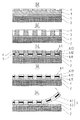
FIGS. 1a to 1 k represent partial cross sections through auxiliary layers and layers of an embodiment of a multilayer structure in accordance with the following invention following various process steps of a process in accordance with the present invention;
FIG. 2 is a view from above of the multilayer structure of FIG. 1k with a metal foil enclosing the multilayer structure;
FIG. 3a shows a partial cross section through the multilayer structure of FIG. 1k with schematically indicated electron beams;
FIG. 3b represents the intensity distribution of the electron beams over the location after passing the multilayer structure of FIG. 1k; and
FIGS. 4a and 4 b show scanning electron microscope images of structures in cross section formed by the multilayer structure of FIG. 1k.
DETAILED DESCRIPTION OF THE PREFERRED EMBODIMENTS
The basic progression of the method of the present invention is represented by an exemplary embodiment in FIGS. 1a to 1 k. The represented layers are generally not shown to scale. A structure 6 is produced by the example shown, which has 1000 parallel strips 6.1, which are 874 nm wide. The recesses 6.2 in the structure 6 are 150 nm wide. Thus, a period of 1024 nm of the structure 6 results.
In step S1, an auxiliary layer 1 of 100 nm thickness, having an iron-nickel alloy (permalloy) is applied in a vacuum by sputtering to a polished and cleaned substrate 2 made of glass, so that a layer structure in accordance with FIG. 1a is created. Alternatively to the material glass it is also possible, for example, to use a corresponding glass-ceramic material, or also steel.
In the next process step S2, an approximately 1.5 μm thick etchable layer 3 is applied to this auxiliary layer 1 and in this example it includes a photosensitive lacquer (FIG. 1b). The spin-coating process is used as the process for the application. In this case a photosensitive lacquer is placed centered on the auxiliary layer 1 and is then distributed by a lacquer centrifuge, so that the etchable layer 3 of even thickness is created. Thereafter the lacquer is dried in an ambient air drying cabinet. In this example the etchable layer 3 includes a positive lacquer. It is basically also possible to alternatively employ a negative lacquer. Otherwise, with this method it is also possible to use a material for the etchable layers 3 which does not react to radiation, but can be easily removed by etching, or developing. Known photosensitive lacquers are well suited as the material for the etchable layer 3.
The subsequent process step S3 includes the application of a 30 nm thick TiO2 layer 4 on the etchable layer 3 by sputtering. The layer structure produced in this way is represented in partial cross section in accordance with FIG. 1c. It is also possible to select a vaporization process, for example, alternatively to the sputtering process. TiO2 was selected as the layer material in this example, because this material is seldom attacked in the subsequent etching processes using conventional etching media. It would correspondingly also be possible to use layers of chromium or SiO2, etc., as the replacement of TiO2.
Thereafter, in process step S4 a photosensitive lacquer layer 5 of a thickness of approximately 200 nm is applied on the TiO2 layer 4 and is evenly distributed, similar to the process step S2, by a spin-coating process (FIG. 1d). In this example the photosensitive lacquer layer 5 includes a positive lacquer, but it is possible here, too, to use a negative lacquer.
In a subsequent process step S5, the photosensitive lacquer layer 5 is locally exposed to UV radiation through a lithographic mask, so that a pattern of straight parallel strips is created in the area of the structure 6, which will be formed later. Alternatively to the use of UV radiation it is also possible to employ a different type of radiation known in connection with lithography methods. Thus it is also possible here to provide the exposure by light in the visible range.
The exposed areas of the photosensitive lacquer layer 5 are removed with the aid of a developing process so that, as represented in FIG. 1e, the TiO2 layer is exposed in small rectangular areas. A photosensitive lacquer developer can be used in this example as the washing medium for the developing process.
The above mentioned previously exposed areas of the TiO2 layer 4 are removed in process step 61 by plasma-etching (“reactive ion etching”) with a fluorine-containing medium. In other words, the TiO2 layer 4 is locally opened (FIG. 1f). In this case fluorine-containing etching media, such as CHF3 gas, CF4 gas, CBrF3 gas or SF6 gas, are used. However, in the same way it is also alternatively possible to use other conventional etching media, for example including chlorine compounds, such as SiCl4.
The remaining photosensitive lacquer of the photosensitive lacquer layer 5 is then removed in process step S62 by ashing with the aid of an oxygen plasma method (FIG. 1g).
Thereafter the second part of the plasma etching process is performed in process step S63, wherein in accordance with FIG. 1h the electrically non-conducting TiO2 layer 4 is used as etching mask, so to speak.
The process parameters are set in process step S63 in such a way that a desired ratio of the depth etching speed to the lateral etching speed is achieved. In this way underetching, which is desirable to a certain extent, is achieved in this way, so that the strips 6.1 to be formed later has a cross-sectional profile which is optimal for the electron-optical function of the structure 6. The auxiliary layer 1, including the iron-nickel alloy, is also used as an etch stop layer in process step S63. As soon as the appropriate surfaces of the auxiliary layer 1 have been etched free, the end of the plasma etching process is signaled. An oxygen plasma, which is mixed with a fluorine-containing gas, is used here as the etching medium.
The two-stage plasma etching process, together with the use of the TiO2 layer 4 as the etching mask, has the advantage that it is possible to obtain high aspect ratios in the etchable layer 3. Aspect ratio is understood to be the quotient of processing depth to the width of the recess 6.2. In this example, aspect ratios of approximately 1.5 μm/150 nm=10 are achieved.
FIG. 1h shows that at the end of the etching processes only those remnants of the etchable layer 3 have remained on the auxiliary layer 1, which are now used as borders for the strips 6.1 to be formed. As the first measure of process step S7, a first gold layer 6.11 of a thickness of approximately 540 nm is applied in a galvanic process. The auxiliary layer 1 is used here as the cathode, whose surface is not oxidized in spite of the previous etching process in process step S63, so that it still has satisfactory electrical conductivity for the galvanizing current.
Following this, a nickel layer 6.12, only approximately 120 nm thick, is applied, also galvanically, on the first gold layer 6.11. Finally, a second gold layer 6.13 of approximately 540 nm thickness, is generated on the nickel layer 6.12 in the following step. Because of the desired beveled shape of the strips 6.1, the second gold layer 6.13 is somewhat wider than the first gold layer 6.11. Note that the nickel material of layer 6.12 can be replaced by copper.
By this layer structure it is possible to form a self-supporting structure 6 of a strip height h of 1.2 μm, which is capable of completely absorbing electron beams 8 (see FIG. 3b) of an energy of 20 keV. In this connection the layer, or sandwich, design of the structure 6 is important. The electron beams 8 are absorbed to a sufficient degree by the first gold layer 6.11 and the second gold layer 6.13. But a single-layer gold layer of approximately 1 μm thickness would not be dimensionally stable, or self-supporting. For this reason the nickel layer 6.12 is provided in the center of the structure 6 between the first gold layer 6.11 and the second gold layer 6.13 for stabilizing the structure 6.
After the buildup of the layers of the multi-layered structure 6 is finished with the strips 6.1, the remaining material of the etchable layer 3 can be removed in process step S8, so that a partial cross section in accordance with FIG. 1j is created. With the represented example, a developing step with a base is again used for this purpose. Alternatively to this it is also possible to use an oxygen plasma, for example, for removing the photosensitive lacquer material.
Finally the structure 6 with a strip height h=1.2 μm can be safely pulled off the auxiliary layer 1, without fissures being created in the structure 6 (FIG. 1k). For the damage-free release of the structure 6 from the auxiliary layer 1 it is necessary that the adhesive forces between the structure 6 and the auxiliary layer 1 are not excessive. This property of the auxiliary layer 1 is called release property. When using sputtering techniques, surface structures, which are particularly advantageous for the mentioned release property, are formed on the auxiliary layer 1 in process step S1.
Although a two-stage etching process is employed in the described example, the present invention is not limited to this type of operation. It is also possible to perform a one-stage etching process.
In accordance with FIG. 2, a finished structure 6 is enclosed in a metal foil 7. Primarily the metal foil 7 is used for easing the handling of the structure 6, in particular for the draw-off process and for the later use of the structure 6 in accordance with the purpose. The structure 6 and the metal foil 7 are produced in one manufacturing process and therefore have the same layer structure. Thus, in this example the structure 6 is only a special area of the metal foil 7 with the recesses 6.2.
However, the layer structure can also be produced in such a way that, for improving the mechanical stability of the structure 6 and of the metal foil 7 enclosing the structure 6, further layers are applied which, for example, have a net-like shape.
A structure 6 is represented (not to scale) in FIG. 3a, whose strips 6.1 have an optimized cross-sectional profile. The associated diagram, in which the radiation intensity at the location x has been indicated, is represented in FIG. 3b.
Important advantages of the structure 6 in accordance with the present invention can be easily seen in this exemplary embodiment by the resulting intensity distribution. For one, practically no radiation can be found in relatively large areas in the shadow of the strips 6.1, this means that the strips 6.1 absorb almost the entire radiation. This occurs for one because of the selection of the material of the layers 6.11 and 6.13 (gold), and also because of the comparatively thick layer structure made possible by the galvanic method. Moreover, the cross-sectional shape of the strips 6.1 plays a substantial role in the maintenance of an appropriate intensity distribution. By the undercut strips 6.1 it is avoided that noticeable reflections of the electron beams 8 are created at the walls of the strips 6.1 which border the recesses 6.2.
The above mentioned reasons inter alia contribute to the fact that a comparatively sharp intensity distribution of the radiation is achieved. Currently customary structures have, for example because of their different cross-sectional profiles, strip edge embodiments and layer thicknesses, a much flatter intensity distribution, i.e. that no such pronounced intensity differences can be noted at the transition from a strip 6.1 to a recess 6.2.
Added to this is that, because of the production method, very straight and smooth strip edges 6.14 and 6.15 in the direction perpendicular to the drawing plane are achieved. In comparison to this, when applying comparative structures by means of the sputter process, a course of the edges is created, which is wavy, or serrated, perpendicular to the drawing plane. The cause of this is that with sputtering an increased layer buildup is always noted in the edge areas, because material is there also deposited on the border walls. When removing the border walls, these deposits break off in an accidental pattern, so that a correspondingly irregular course of the edges in the longitudinal direction is created.
The present invention is not limited to the three-layered structure 6 represented in the exemplary embodiment, but also includes structures 6 of two, four or more layers of the most diverse material and sequences of rows of layers. A preferred embodiment of the present invention is a structure 6 with a symmetrical layer buildup, wherein in this connection the symmetry is to be related to the selection of the material (Au—Ni—Au in the represented example) and/or to the layer thickness (540 nm-120 nm-540 nm in the example represented).
A scanning electron microscope photograph is represented in FIG. 4a, in which a partial cross section through the strips 6.1, through the limiting layers of the etchable layer 3, as well as through the auxiliary layer 1 and through the support substrate 2, is represented. The representation corresponds to FIG. 1i.
FIG. 4b shows a partial cross section through the strips 6.1 following their release from the auxiliary layer 1.
Within the scope of the present invention, further embodiment variations of course also exist besides the explained example.

Claims (13)

We claim:
1. A method for producing a self-supporting electron-optical transparent structure comprising multi-layer-strips and recesses located between said multi-layer strips, said method comprising:
applying a first layer to a second layer;
presetting a pattern;
etching said pattern out of said first layer so that partial areas of said second layer are uncovered;
galvanically applying layers to said uncovered partial areas of said second layer so that multi-layer strips are formed thereon and an electron-optical transparent structure is formed; and
removing said electron-optical transparent structure off said second layer.
2. The method in accordance with claim 1, wherein following said applying said first layer to said second layer and prior to etching said pattern out of said first layer the following are performed:
applying a third layer to said first layer;
covering said third layer with a photosensitive lacquer layer;
exposing or irradiating said photosensitive lacquer layer in accordance with said pattern; and
removing at least partially said photosensitive lacquer layer and said third layer by an etching process.
3. The method in accordance with claim 1, wherein said first layer is removed prior to said removing said electron-optical transparent structure off said second layer.
4. The method in accordance with claim 1, further comprising applying said second layer to a support substrate.
5. The method in accordance with claim 4, wherein said second layer is applied to said support substrate by a sputter process.
6. The method in accordance with claim 1, wherein said multi-layer strips comprise at least one gold layer.
7. The method in accordance with claim 1, wherein said multi-layer strips comprise at least one nickel layer.
8. The method in accordance with claim 1, wherein said multi-layer strips comprise a copper layer.
9. The method in accordance with claim 1, wherein said second layer comprises an iron-nickel alloy.
10. A self-supporting electron-optical transparent structure comprising multi-layer strips and recesses located between said multi-layer strips, said structure made by a process comprising:
applying a first layer to a second layer;
presetting a pattern;
etching said pattern out of said first layer so that partial areas of said second layer are uncovered;
galvanically applying layers to said uncovered partial areas of said second layer so that multi-layer strips are formed thereon and an electron-optical transparent structure is formed; and
removing said electron-optical transparent structure off said second layer.
11. The self-supporting electron-optical transparent structure in accordance with claim 10, wherein said multi-layer strips comprise at least one nickel layer and at least one gold layer.
12. The self-supporting electron-optical transparent structure in accordance with claim 10, wherein said multi-layer strips comprise a copper layer and at least one gold layer.
13. The self-supporting electron-optical transparent structure in accordance accordance with claim 10, wherein widths of said multi-layer strips are changed in a direction of height of said multi-layer strips.
US10/209,186 2001-07-31 2002-07-31 Method for producing a self-supporting electron-optical transparent structure, and structure produced in accordance with the method Expired - Fee Related US6800404B2 (en)

Applications Claiming Priority (3)

Application Number Priority Date Filing Date Title
DE10137493.3 2001-07-31
DE10137493 2001-07-31
DE10137493A DE10137493A1 (en) 2001-07-31 2001-07-31 Method for producing a self-supporting structure which can be irradiated electron-optically and structure produced using the method

Publications (2)

Publication Number Publication Date
US20030036022A1 US20030036022A1 (en) 2003-02-20
US6800404B2 true US6800404B2 (en) 2004-10-05

Family

ID=7693862

Family Applications (1)

Application Number Title Priority Date Filing Date
US10/209,186 Expired - Fee Related US6800404B2 (en) 2001-07-31 2002-07-31 Method for producing a self-supporting electron-optical transparent structure, and structure produced in accordance with the method

Country Status (2)

Country Link
US (1) US6800404B2 (en)
DE (1) DE10137493A1 (en)

Families Citing this family (1)

* Cited by examiner, † Cited by third party
Publication number Priority date Publication date Assignee Title
TWI577248B (en) * 2016-07-19 2017-04-01 欣興電子股份有限公司 Circuit carrier and manufacturing mtheod thereof

Citations (6)

* Cited by examiner, † Cited by third party
Publication number Priority date Publication date Assignee Title
DE1521476A1 (en) 1965-09-16 1969-07-31 Siemens Ag Method and device for the production of foil diaphragms, in particular aperture diaphragms for electron microscopes
DE2344111C2 (en) 1973-08-29 1975-10-02 Siemens Ag, 1000 Berlin Und 8000 Muenchen Process for the production of a screen for corpuscular beam devices and screen produced according to this process
US4061814A (en) * 1974-04-03 1977-12-06 Siemens Aktiengesellschaft Method and masking structure for configurating thin layers
US4080267A (en) * 1975-12-29 1978-03-21 International Business Machines Corporation Method for forming thick self-supporting masks
US4497884A (en) * 1981-10-01 1985-02-05 Veb Zentrum Fur Forschung Und Technologie Mikroelektronik Method for the production of a self-supporting mask
US5858576A (en) 1993-10-22 1999-01-12 Sanyo Electric Co., Ltd. Stencil mask for photochemical reaction process and method of making the same

Patent Citations (6)

* Cited by examiner, † Cited by third party
Publication number Priority date Publication date Assignee Title
DE1521476A1 (en) 1965-09-16 1969-07-31 Siemens Ag Method and device for the production of foil diaphragms, in particular aperture diaphragms for electron microscopes
DE2344111C2 (en) 1973-08-29 1975-10-02 Siemens Ag, 1000 Berlin Und 8000 Muenchen Process for the production of a screen for corpuscular beam devices and screen produced according to this process
US4061814A (en) * 1974-04-03 1977-12-06 Siemens Aktiengesellschaft Method and masking structure for configurating thin layers
US4080267A (en) * 1975-12-29 1978-03-21 International Business Machines Corporation Method for forming thick self-supporting masks
US4497884A (en) * 1981-10-01 1985-02-05 Veb Zentrum Fur Forschung Und Technologie Mikroelektronik Method for the production of a self-supporting mask
US5858576A (en) 1993-10-22 1999-01-12 Sanyo Electric Co., Ltd. Stencil mask for photochemical reaction process and method of making the same

Also Published As

Publication number Publication date
DE10137493A1 (en) 2003-04-10
US20030036022A1 (en) 2003-02-20

Similar Documents

Publication Publication Date Title
US4244799A (en) Fabrication of integrated circuits utilizing thick high-resolution patterns
US4592801A (en) Method of patterning thin film
TWI846616B (en) Mask blank, phase shift mask and method of manufacturing a semiconductor device
US4174219A (en) Method of making a negative exposure mask
GB2040498A (en) Method of forming a microscopic pattern and an electronic device including such a pattern
EP0644462B1 (en) Reactive ion beam etching of gratings and cross gratings structures
US20040241559A1 (en) Hardmask/barrier layer for dry etching chrome films and improving post develop resist profiles on photomasks
US4329410A (en) Production of X-ray lithograph masks
US4954717A (en) Photoelectron mask and photo cathode image projection method using the same
EP0953876A2 (en) Process for fabricating a lithographic mask
US5567551A (en) Method for preparation of mask for ion beam lithography
US9250514B2 (en) Apparatus and methods for fabricating a photomask substrate for EUV applications
US6800404B2 (en) Method for producing a self-supporting electron-optical transparent structure, and structure produced in accordance with the method
US6365326B1 (en) Pattern density tailoring for etching of advanced lithographic mask
JPH0466345B2 (en)
JPH03174724A (en) Method of forming pattern
US4497884A (en) Method for the production of a self-supporting mask
US5178975A (en) High resolution X-ray mask having high aspect ratio absorber patterns
EP0518545A1 (en) Dry lithographic etching with gaseous mixtures of oxygen and chlorine
JP2531608B2 (en) Method for manufacturing semiconductor device
JPH09306822A (en) Plasma etching method and photomask manufacturing method
KR100869546B1 (en) Method of fabricating thin film pattern using atomic force microscopy lithography
Gruhle et al. Deep-uv lithography mask fabrication with 200nm feature size using a liftoff technique
US20080203386A1 (en) Method of forming a patterned resist layer for patterning a semiconductor product
JP3513315B2 (en) Method of manufacturing field emission electronic device

Legal Events

Date Code Title Description
AS Assignment

Owner name: DR. JOHANNES HEIDENHAIN GMBH, GERMANY

Free format text: ASSIGNMENT OF ASSIGNORS INTEREST;ASSIGNORS:SPECKBACHER, PETER;FLATSCHER, GEORG;ALLGAUER, MICHAEL;AND OTHERS;REEL/FRAME:013440/0311;SIGNING DATES FROM 20021007 TO 20021010

FEPP Fee payment procedure

Free format text: PAYOR NUMBER ASSIGNED (ORIGINAL EVENT CODE: ASPN); ENTITY STATUS OF PATENT OWNER: LARGE ENTITY

FPAY Fee payment

Year of fee payment: 4

FPAY Fee payment

Year of fee payment: 8

REMI Maintenance fee reminder mailed
LAPS Lapse for failure to pay maintenance fees
STCH Information on status: patent discontinuation

Free format text: PATENT EXPIRED DUE TO NONPAYMENT OF MAINTENANCE FEES UNDER 37 CFR 1.362

FP Lapsed due to failure to pay maintenance fee

Effective date: 20161005