US6763504B2 - Method for reducing RC parasitics in interconnect networks of an integrated circuit - Google Patents
Method for reducing RC parasitics in interconnect networks of an integrated circuit Download PDFInfo
- Publication number
- US6763504B2 US6763504B2 US10/237,328 US23732802A US6763504B2 US 6763504 B2 US6763504 B2 US 6763504B2 US 23732802 A US23732802 A US 23732802A US 6763504 B2 US6763504 B2 US 6763504B2
- Authority
- US
- United States
- Prior art keywords
- nodes
- resistor
- node
- shorting
- network
- Prior art date
- Legal status (The legal status is an assumption and is not a legal conclusion. Google has not performed a legal analysis and makes no representation as to the accuracy of the status listed.)
- Expired - Fee Related, expires
Links
Images


Classifications
-
- G—PHYSICS
- G06—COMPUTING OR CALCULATING; COUNTING
- G06F—ELECTRIC DIGITAL DATA PROCESSING
- G06F30/00—Computer-aided design [CAD]
- G06F30/30—Circuit design
- G06F30/36—Circuit design at the analogue level
- G06F30/367—Design verification, e.g. using simulation, simulation program with integrated circuit emphasis [SPICE], direct methods or relaxation methods
Definitions
- This invention is related to the field of design automation, and more particularly, to a method for reducing the size of RC parasitics of interconnect networks in an integrated circuit (IC) in order to reduce circuit analysis time.
- An integrated circuit can be represented by a collection of transistors with the terminals interconnected by nets. After completing the layout, each net is electrically modeled as an RC network of nodes and elements.
- the elements of the network are resistors (Rs) and capacitors (Cs). Nodes connecting transistor terminals are referred to boundary nodes, while the remaining ones are referred to as internal nodes of the RC network.
- C is the grounded capacitance of the node and ⁇ is the total conductance (i.e., the inverse of the resistance) connected to the node.
- ⁇ is the total conductance (i.e., the inverse of the resistance) connected to the node.
- FIG. 2 is an illustration of the node elimination process for node X in the example given in FIG. 1 .
- Elmore delays at all boundary nodes are preserved by the elimination process.
- Elmore's delay is the first time-moment of the impulse response at a sink.
- the response at a sink due to an arbitrary input waveform is simply the convolution of the impulse response with the input waveform). This is highly regarded property of the RC reduction process.
- Internal node elimination is generally restricted to only those nodes that have a fill-in count of 0 or less to preserve the sparsity of the reduced RC network, since the total number of resistors cannot increase.
- circuits which contain large RC networks with many boundary nodes and a wide range (over seven orders of magnitude) of time constants are routinely encountered. Since algorithms in the prior art only eliminate internal nodes, their quality is limited since there usually remains a large number of boundary nodes with very small time constants (several orders of magnitude less than the Elmore delay).
- an object of the invention to reduce large parasitic RC networks in the interconnect of an integrated circuit design, preferably after having applied internal node elimination techniques (or any other RC reduction technique).
- the speed of the circuit analysis tools is the fastest at this extreme limit.
- a method for allowing further reduction of parasitic RC networks after applying conventional internal node elimination techniques is provided.
- the present inventive method further reduces (beyond only eliminating internal nodes) RC networks by shorting certain resistors connected to the boundary nodes, and adjusting the value of neighboring resistors to compensate for the errors introduced by the shorting.
- This additional reduction of the RC networks greatly improves the performance of downstream analysis tools, such as circuit simulators, without a significant loss of accuracy.
- a resistor is selected as a candidate for shorting if the accumulated delay error at either end is less than a predetermined threshold.
- This threshold is a fraction (e.g., ⁇ fraction (1/10) ⁇ ) of the time-constant threshold chosen for the internal node elimination conventional technique in order to limit the growth of the accumulated delay error.
- the accumulated delay error at the merged node is updated and values of downstream resistors are changed to preserve the delay at downstream nodes.
- An important aspect of the invention is the simplicity of the formula used to change the downstream resistor value, namely, the product of the value of the resistor shorted and the ratio of the cumulative down stream capacitors of the two ends of the resistor whose value is being changed. This particular choice of updating the downstream resistor values minimizes the absolute-value of the delay errors at every node due to shorting of the selected resistor.
- a method for reducing the size of RC parasitics in an interconnect network of an integrated circuit the IC being formed as a collection of transistors, each having its terminals interconnected by nets, each of the nets modeled by nodes and elements, the elements modeled as resistors (R) and capacitors (C), the nodes attached to transistor terminals labeled as boundary nodes while the remaining nodes are labeled as internal nodes, the method including the steps of: a) selecting a net from the collection of nets; b) reducing the size of the RC network of the selected net by eliminating the internal nodes having a time-constant below a predetermined threshold and a fill-in count contained within a pre-specified limit; c) iteratively shorting a resistor connected to a boundary node, wherein the accumulated delay error at the boundary node after shorting is less than a fraction of the predetermined threshold; d) updating the values of the resistors adjoining the
- FIG. 1 is a schematic diagram defining a conventional nodal time constant.
- FIG. 2 shows schematically how an internal node is typically eliminated by conventional techniqus.
- FIG. 3 shows an example of a conventional boundary node.
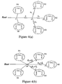
- FIG. 4 is a schematic diagram that illustrates the reduction of RC parasitics in a interconnect network, in accordance with the present invention, wherein FIG. 4 a shows the RC tree before shorting the resistor between A and B, and FIG. 4 b showing the RC tree after shorting the same branch.
- FIG. 5 is a flow chart illustrating the major steps of the RC reduction algorithm, according to the present invention.
- FIG. 6 is a schematic diagram of a sample resistor-capacitor network.
- FIG. 7 through FIG. 13 are respectively schematic diagrams showing the circuit of FIG. 6 after shorting resistor R A (FIG. 7 ); after shorting resistor R B (FIG. 8 ); after shorting resistor R C (FIG. 9 ); after shorting resistor R D , R E , R F , R G , R H , and R I (FIG. 10 ); after shorting R X (FIG. 11 ); after shorting R Y (FIG. 12 ); and after shorting R Z (FIG. 13 ).
- Table 1 in FIG. 14 shows the performance measurement of the invented algorithm when compared with the algorithm that only eliminates internal nodes.
- the algorithm of the present invention starts by applying a conventional internal node elimination method to a given RC network with a predefined time-constant threshold and fill-in count limit. Thereafter, all the nodes left in the RC network are either boundary nodes or internal nodes with either time constants or fill-in counts too large to be safely eliminated.
- a Root node namely, the source or driver of the RC tree
- an RC tree is characterized in that there exists a unique path of resistors from the Root node to any other node, e.g. X, in the tree.
- the node Y adjacent to X on this path will be referred to as the parent.
- X is a child of Y.
- a node may have several children, but will always have a unique parent.
- C X denote the grounded capacitance at any arbitrarily selected node X in the tree, and C X represent the cumulative downstream capacitance at node X and all its descendants in the tree (i.e., children, children's children, etc.).
- resistor R between nodes A (parent) and B (child) in the tree shown in FIG. 4 a is to be shorted.
- J denote any child (there could be several) connected via resistor R J to B.
- Node B is shown as having three children, J 1 , J 2 , and J 3 .
- ⁇ AB max( ⁇ A , ⁇ B +R C B ) (14)
- the threshold for accumulated error be a small fraction ( e . g . , 1 10 )
- merging of boundary nodes is carried out only if the accumulated error does not exceed, e.g., 1 10 ,
- a step-by-step process for carrying out the invented RC reduction algorithm is given in the flow chart shown in FIG. 5 .
- the processing steps are labeled T 0 through T 6 for easy reference.
- Step T 0 The process begins (Step T 0 ) by providing an RC network, a time-constant threshold ⁇ max and a fill-in count limit. Then, all internal nodes with fill-in count within a predetermined limit and nodal time-constant ⁇ max are eliminated.
- Step T 1 a boundary node driving the RC network is designated the Root, and a minimum resistive spanning tree is created so that Equations 8 and 9 are satisfied for all resistors within the context of the tree.
- Step T 2 It algorithm then determines if there exists any boundary node in the RC network that can be processed (Step T 2 ) and, if so, it selects a node in Step T 3 , and calculates the accumulated error ⁇ AB using Equation 14 if the resistor between the selected node and its parent node is to be shorted.
- Step T 4 the value of ⁇ AB calculated in the previous step is compared against ⁇ fraction (1/10) ⁇ max . If ⁇ AB ⁇ fraction (1/10) ⁇ max , the process skips the selected node for processing and returns to Step T 2 to select a new boundary node for processing.
- Step T 5 the algorithm actually shorts the resistor between the selected node and its parent and updates the value of the accumulated error at the merged node (due to shorting) in Step T 5 .
- Step T 6 perturbations are introduced at all neighboring downstream children resistors using Equation 11, which completes the processing of one boundary node in the RC network.
- the algorithm then returns to Step T 2 to select the next node,. And comes to a stop when all boundary nodes in the circuit have been considered. This completes the reduction of a single RC network.
- the same approach is now applied to another RC network, and so on.
- FIG. 6 To illustrate how the inventive RC reduction method carried out for an RC network, the circuit in FIG. 6 will now show the transformation of the network during RC reduction.
- There are 14 nodes in the circuit namely, A, B, C, D, E, F, G, H, I, S, T, X, Y, and Z.
- Node S is the source driving the network and is designated the Root.
- Nodes A, B, C, D, E, F, G, H, and I are boundary nodes, i.e., there is an external connection (transistor terminal) at each of the nodes, (not shown).
- Step T 0 cannot eliminate any internal node since each of the four internal nodes X, Y, Z, and T have fill-in count of two, hence, greater than zero.
- Each resistor in the RC network is assumed to be 1 ⁇ .
- Each boundary node has a grounded capacitance of 10 ⁇ F while each internal node has a grounded capacitance of 1 fF. Since the network of FIG. 6 is already an RC tree, nothing is done in Step T 1 .
- Step T 2 the merged node obtained by shorting a resistor between a node and its parent will be denoted by the name of parent (without concatenating the names of the two ends of the resistor).
- Step T 2 the process begins with Step T 2 , with node A (with parent X) the first node to be selected for processing, and resistor R A , the first resistor selected for shorting.
- FIG. 7 shows the circuit after shoring R A .
- the combined capacitance value at node X becomes 11 fF due to shorting of R A .
- the algorithm selects boundary node B (Step T 2 ) and short R B in Steps T 3 , T 4 , T 5 , and T 6 , with the resulting circuit shown in FIG. 8 .
- the grounded capacitor at node B is added to the capacitance value at the parent node X resulting in a total capacitance of 21fF.
- the accumulated error at node X remains at 0.01 ps since the error contribution from shorting R B is the same as the existing error accumulated on node X and the algorithm takes the maximum between the two values in Equation 14.
- the circuit is shown after selecting node C and shorting R C .
- the capacitance at node X is once again incremented by the amount of the capacitance at node C and the accumulated error at node X remains unchanged for the same reason as when R B was shorted. It is evident that what occurs to node Y and node Z when R D , R E , R F , R G , R H , and R I are shorted is identical to what happened to node X when R A , R B , and R C were shorted, due to the similarities at nodes X, Y, and Z in terms of their RC interconnections.
- Efficiency is measured by the amount of run-time reduction of the transistor-level static timing analysis, and accuracy is determined by the amount of stage delay error (i.e., the delay of the gate driving the RC interconnect network at the root added to the delay from the root to a boundary (or sink) node of the RC network caused by the reduced RC networks created by the algorithm.
- stage delay error i.e., the delay of the gate driving the RC interconnect network at the root added to the delay from the root to a boundary (or sink) node of the RC network caused by the reduced RC networks created by the algorithm.
- stage delay error i.e., the delay of the gate driving the RC interconnect network at the root added to the delay from the root to a boundary (or sink) node of the RC network caused by the reduced RC networks created by the algorithm.
- the measurements resulting from the different values of the user-selected time-constant threshold ⁇ max are tabulated in Table 1 in FIG. 14 .
- Table 1 The measurements resulting from the different values of the user-selected time-constant threshold ⁇ max are tabulated in Table 1 in FIG. 14 .
- the first section shows the results from running only the internal node elimination Step T 0 of the algorithm, and is to be used for comparison purposes.
- the second section shows the results from running all the steps, from Steps T 0 through T 6 .
- the present invention can be realized in hardware, software, or a combination of hardware and software.
- the present invention can be realized in a centralized fashion in one computer system, or in a distributed fashion where different elements are spread across several interconnected computer systems. Any kind of computer system—or other apparatus adapted for carrying out the methods described herein—is suitable.
- a typical combination of hardware and software could be a general purpose computer system with a computer program that, when being loaded and executed, controls the computer system such that it carries out the methods described herein.
- the present invention can also be embedded in a computer program product, which comprises all the features enabling the implementation of the methods described herein, and which—when loaded in a computer system—is able to carry out the method of the present inventiion.
- Computer program in the present context is defined as any expression, in any language, code or notation, of a set of instructions intended to cause a system having an information processing capability to perform a particular function either directly or after conversion to another language, code or notation and/or reproduction in a different material form.
Landscapes
- Engineering & Computer Science (AREA)
- Computer Hardware Design (AREA)
- Physics & Mathematics (AREA)
- Theoretical Computer Science (AREA)
- Microelectronics & Electronic Packaging (AREA)
- Evolutionary Computation (AREA)
- Geometry (AREA)
- General Engineering & Computer Science (AREA)
- General Physics & Mathematics (AREA)
- Design And Manufacture Of Integrated Circuits (AREA)
Abstract
Description


Claims (10)


Priority Applications (1)
| Application Number | Priority Date | Filing Date | Title |
|---|---|---|---|
| US10/237,328 US6763504B2 (en) | 2002-09-06 | 2002-09-06 | Method for reducing RC parasitics in interconnect networks of an integrated circuit |
Applications Claiming Priority (1)
| Application Number | Priority Date | Filing Date | Title |
|---|---|---|---|
| US10/237,328 US6763504B2 (en) | 2002-09-06 | 2002-09-06 | Method for reducing RC parasitics in interconnect networks of an integrated circuit |
Publications (2)
| Publication Number | Publication Date |
|---|---|
| US20040049746A1 US20040049746A1 (en) | 2004-03-11 |
| US6763504B2 true US6763504B2 (en) | 2004-07-13 |
Family
ID=31990788
Family Applications (1)
| Application Number | Title | Priority Date | Filing Date |
|---|---|---|---|
| US10/237,328 Expired - Fee Related US6763504B2 (en) | 2002-09-06 | 2002-09-06 | Method for reducing RC parasitics in interconnect networks of an integrated circuit |
Country Status (1)
| Country | Link |
|---|---|
| US (1) | US6763504B2 (en) |
Cited By (13)
| Publication number | Priority date | Publication date | Assignee | Title |
|---|---|---|---|---|
| US20060031055A1 (en) * | 2004-04-07 | 2006-02-09 | Sheehan Bernard N | Branch merge reduction of RLCM networks |
| US20070044051A1 (en) * | 2005-08-17 | 2007-02-22 | Cadence Design Systems, Inc. | Method and system for validating a hierarchical simulation database |
| US7350167B1 (en) | 2003-08-01 | 2008-03-25 | Cadence Design Systems, Inc. | Extraction and reduction of capacitor elements using matrix operations |
| US7373620B1 (en) | 2003-08-01 | 2008-05-13 | Cadence Design Systems, Inc. | Methods and mechanisms for extracting and reducing capacitor elements |
| US7448010B1 (en) * | 2003-08-01 | 2008-11-04 | Cadence Design Systems, Inc. | Methods and mechanisms for implementing virtual metal fill |
| US20090026620A1 (en) * | 2007-05-15 | 2009-01-29 | Sharp Kabushiki Kaisha | Method for cutting multilayer substrate, method for manufacturing semiconductor device, semiconductor device, light emitting device, and backlight device |
| US20090271166A1 (en) * | 2008-04-28 | 2009-10-29 | Sun Microsystems, Inc. | Systems and methods for current analysis of circuits including relatively large rc networks |
| US20110016442A1 (en) * | 2009-07-16 | 2011-01-20 | International Business Machines Corporation | Method of Performing Static Timing Analysis Considering Abstracted Cell's Interconnect Parasitics |
| US7900164B1 (en) * | 2004-01-16 | 2011-03-01 | Alters Corporation | Structure to measure both interconnect resistance and capacitance |
| US8392867B2 (en) | 2011-01-13 | 2013-03-05 | International Business Machines Corporation | System, method and program storage device for developing condensed netlists representative of groups of active devices in an integrated circuit and for modeling the performance of the integrated circuit based on the condensed netlists |
| US8893064B1 (en) | 2013-06-24 | 2014-11-18 | International Business Machines Corporation | System and method for determining merged resistance values for same-type terminals in a complex semiconductor structure |
| US10169514B2 (en) | 2017-01-18 | 2019-01-01 | International Business Machines Corporation | Approximation of resistor-capacitor circuit extraction for thread-safe design changes |
| US10402532B1 (en) * | 2016-04-07 | 2019-09-03 | Cadence Design Systems, Inc. | Methods, systems, and computer program products for implementing an electronic design with electrical analyses with compensation circuit components |
Families Citing this family (4)
| Publication number | Priority date | Publication date | Assignee | Title |
|---|---|---|---|---|
| US7243313B1 (en) * | 2003-11-24 | 2007-07-10 | Cadence Design Systems, Inc. | System and method for reducing the size of RC circuits |
| US7346874B1 (en) * | 2004-01-30 | 2008-03-18 | Magma Design Automation, Inc. | Parametric timing analysis |
| US10068044B1 (en) * | 2016-12-19 | 2018-09-04 | Cadence Design Systems, Inc. | System and method for efficient device testing and validation of fast transients |
| CN116205011B (en) * | 2021-11-30 | 2026-02-10 | 浙江大学 | A method for reducing the size of large-scale RC networks based on the TICER algorithm |
Citations (4)
| Publication number | Priority date | Publication date | Assignee | Title |
|---|---|---|---|---|
| US5751593A (en) * | 1996-04-10 | 1998-05-12 | Motorola, Inc. | Accurate delay prediction based on multi-model analysis |
| US5790415A (en) * | 1996-04-10 | 1998-08-04 | Pullela; Satyamurthy | Complementary network reduction for load modeling |
| US5875114A (en) * | 1996-08-27 | 1999-02-23 | Mitsubishi Denki Kabushiki Kaisha | Interconnect delay calculation apparatus and path delay value verification apparatus for designing semiconductor integrated circuit and circuit model data storage device |
| US6374205B1 (en) * | 1998-02-13 | 2002-04-16 | Kabushiki Kaisha Toshiba | Method of reducing circuit data, method of simulating circuit, and medium for storing circuit data reduction program |
-
2002
- 2002-09-06 US US10/237,328 patent/US6763504B2/en not_active Expired - Fee Related
Patent Citations (4)
| Publication number | Priority date | Publication date | Assignee | Title |
|---|---|---|---|---|
| US5751593A (en) * | 1996-04-10 | 1998-05-12 | Motorola, Inc. | Accurate delay prediction based on multi-model analysis |
| US5790415A (en) * | 1996-04-10 | 1998-08-04 | Pullela; Satyamurthy | Complementary network reduction for load modeling |
| US5875114A (en) * | 1996-08-27 | 1999-02-23 | Mitsubishi Denki Kabushiki Kaisha | Interconnect delay calculation apparatus and path delay value verification apparatus for designing semiconductor integrated circuit and circuit model data storage device |
| US6374205B1 (en) * | 1998-02-13 | 2002-04-16 | Kabushiki Kaisha Toshiba | Method of reducing circuit data, method of simulating circuit, and medium for storing circuit data reduction program |
Non-Patent Citations (7)
| Title |
|---|
| A. J. van Genderen and N. P. van der Meijs, "Extracting Simple but Accurate RC Models for VLSI Interconnect", ISCAS 1988 IEEE, p. 2351-2354. |
| Bernard N. Sheehan, "TICER: Realizable Reduction of Extracted RC Circuits", 1999 IEEE, p. 200-203. |
| Devgan et al., "Realizable Reduction for RC Interconnect Circuits", Nov. 1999, IEEE, ACM international conference on Computer-Aided Design, Digest of Technical Papers, pp. 204-207.* * |
| Ganesh et al., "RC-in RC-out Model Order Reduction Accurate Up to Second Order Moments", Sep. 2001, IEEE, International Conference on Computer Design, Proceedings, pp. 505-506.* * |
| Genderen et al., "Reduced RC Models for IC Interconnections with Coupling Capacitances", Mar. 1992, IEEE, 3<rd >European Conference on Design Automation, Proceedings, pp. 132-136.* * |
| Genderen et al., "Reduced RC Models for IC Interconnections with Coupling Capacitances", Mar. 1992, IEEE, 3rd European Conference on Design Automation, Proceedings, pp. 132-136.* |
| Maffezzoni et al., "Efficient Method for Simulating Time Delay of Distributed Interconnections in VLSI Circuits", Jun. 1999, IEEE Electronic Letters, vol. 35, iss. 12, pp. 976-977.* * |
Cited By (20)
| Publication number | Priority date | Publication date | Assignee | Title |
|---|---|---|---|---|
| US7725859B1 (en) | 2003-08-01 | 2010-05-25 | Cadence Design Systems, Inc. | Methods and mechanisms for inserting metal fill data |
| US8572545B1 (en) | 2003-08-01 | 2013-10-29 | Cadence Design Systems, Inc. | Methods and mechanisms for extracting and reducing capacitor elements |
| US7350167B1 (en) | 2003-08-01 | 2008-03-25 | Cadence Design Systems, Inc. | Extraction and reduction of capacitor elements using matrix operations |
| US7373620B1 (en) | 2003-08-01 | 2008-05-13 | Cadence Design Systems, Inc. | Methods and mechanisms for extracting and reducing capacitor elements |
| US8024677B2 (en) | 2003-08-01 | 2011-09-20 | Cadence Design Systems, Inc. | Methods and mechanisms for inserting metal fill data |
| US7448010B1 (en) * | 2003-08-01 | 2008-11-04 | Cadence Design Systems, Inc. | Methods and mechanisms for implementing virtual metal fill |
| US7900164B1 (en) * | 2004-01-16 | 2011-03-01 | Alters Corporation | Structure to measure both interconnect resistance and capacitance |
| US7774174B2 (en) * | 2004-04-07 | 2010-08-10 | Mentor Graphics Corporation | Branch merge reduction of RLCM networks |
| US20060031055A1 (en) * | 2004-04-07 | 2006-02-09 | Sheehan Bernard N | Branch merge reduction of RLCM networks |
| US7434183B2 (en) * | 2005-08-17 | 2008-10-07 | Cadence Design Systems, Inc. | Method and system for validating a hierarchical simulation database |
| US20070044051A1 (en) * | 2005-08-17 | 2007-02-22 | Cadence Design Systems, Inc. | Method and system for validating a hierarchical simulation database |
| US20090026620A1 (en) * | 2007-05-15 | 2009-01-29 | Sharp Kabushiki Kaisha | Method for cutting multilayer substrate, method for manufacturing semiconductor device, semiconductor device, light emitting device, and backlight device |
| US20090271166A1 (en) * | 2008-04-28 | 2009-10-29 | Sun Microsystems, Inc. | Systems and methods for current analysis of circuits including relatively large rc networks |
| US8200470B2 (en) * | 2008-04-28 | 2012-06-12 | Oracle America, Inc. | Systems and methods for current analysis of circuits including relatively large RC networks |
| US20110016442A1 (en) * | 2009-07-16 | 2011-01-20 | International Business Machines Corporation | Method of Performing Static Timing Analysis Considering Abstracted Cell's Interconnect Parasitics |
| US8122411B2 (en) * | 2009-07-16 | 2012-02-21 | International Business Machines Corporation | Method of performing static timing analysis considering abstracted cell's interconnect parasitics |
| US8392867B2 (en) | 2011-01-13 | 2013-03-05 | International Business Machines Corporation | System, method and program storage device for developing condensed netlists representative of groups of active devices in an integrated circuit and for modeling the performance of the integrated circuit based on the condensed netlists |
| US8893064B1 (en) | 2013-06-24 | 2014-11-18 | International Business Machines Corporation | System and method for determining merged resistance values for same-type terminals in a complex semiconductor structure |
| US10402532B1 (en) * | 2016-04-07 | 2019-09-03 | Cadence Design Systems, Inc. | Methods, systems, and computer program products for implementing an electronic design with electrical analyses with compensation circuit components |
| US10169514B2 (en) | 2017-01-18 | 2019-01-01 | International Business Machines Corporation | Approximation of resistor-capacitor circuit extraction for thread-safe design changes |
Also Published As
| Publication number | Publication date |
|---|---|
| US20040049746A1 (en) | 2004-03-11 |
Similar Documents
| Publication | Publication Date | Title |
|---|---|---|
| US6763504B2 (en) | Method for reducing RC parasitics in interconnect networks of an integrated circuit | |
| Ratzlaff et al. | RICE: Rapid interconnect circuit evaluator | |
| Ratzlaff et al. | RICE: Rapid interconnect circuit evaluation using AWE | |
| Pullela et al. | Skew and delay optimization for reliable buffered clock trees | |
| US5654898A (en) | Timing-driven integrated circuit layout through device sizing | |
| Kuhlmann et al. | Exact and efficient crosstalk estimation | |
| US6314546B1 (en) | Interconnect capacitive effects estimation | |
| Alpert et al. | Wire segmenting for improved buffer insertion | |
| US5313398A (en) | Method and apparatus for simulating a microelectronic circuit | |
| US7676780B2 (en) | Techniques for super fast buffer insertion | |
| US6810506B1 (en) | Methodology for stitching reduced-order models of interconnects together | |
| CN103930891B (en) | Using the existing pre-routing algorithm, using the linear Steiner minimum tree (RSMT) method to determine the length of the line between nodes | |
| US7987439B2 (en) | Method and apparatus for analyzing circuit model by reduction and computer program product for analyzing the circuit model | |
| US6412101B1 (en) | Simultaneous path optimization (SPO) system and method | |
| US6430731B1 (en) | Methods and apparatus for performing slew dependent signal bounding for signal timing analysis | |
| US7251791B2 (en) | Methods to generate state space models by closed forms and transfer functions by recursive algorithms for RLC interconnect and transmission line and their model reduction and simulations | |
| EP0901088A2 (en) | Framework for rules checking | |
| US7774174B2 (en) | Branch merge reduction of RLCM networks | |
| US7594209B2 (en) | Method for incorporating Miller capacitance effects in digital circuits for an accurate timing analysis | |
| Ismail et al. | DTT: direct truncation of the transfer function-an alternative to moment matching for tree structured interconnect | |
| Liao et al. | S-parameter based macro model of distributed-lumped networks using exponentially decayed polynomial function | |
| Hou et al. | CONCERT: A concurrent transient fault simulator for nonlinear analog circuits | |
| US6601223B1 (en) | System and method for fast interconnect delay estimation through iterative refinement | |
| US20030009729A1 (en) | Method for automatically sizing and biasing circuits | |
| US7124388B2 (en) | Methods to generate state space models by closed forms and transfer functions by recursive algorithms for RC interconnect and transmission line and their model reduction and simulations |
Legal Events
| Date | Code | Title | Description |
|---|---|---|---|
| AS | Assignment |
Owner name: INTERNATIONAL BUSINESS MACHINES CORPORATION, NEW Y Free format text: ASSIGNMENT OF ASSIGNORS INTEREST;ASSIGNORS:RAO, VASANT B.;LEDALLA, RAVICHANDER;SOREFF, JEFFREY P.;AND OTHERS;REEL/FRAME:013279/0119;SIGNING DATES FROM 20020905 TO 20020906 |
|
| FEPP | Fee payment procedure |
Free format text: PAYOR NUMBER ASSIGNED (ORIGINAL EVENT CODE: ASPN); ENTITY STATUS OF PATENT OWNER: LARGE ENTITY |
|
| FPAY | Fee payment |
Year of fee payment: 4 |
|
| AS | Assignment |
Owner name: GOOGLE INC., CALIFORNIA Free format text: ASSIGNMENT OF ASSIGNORS INTEREST;ASSIGNOR:INTERNATIONAL BUSINESS MACHINES CORPORATION;REEL/FRAME:026894/0001 Effective date: 20110817 |
|
| FPAY | Fee payment |
Year of fee payment: 8 |
|
| REMI | Maintenance fee reminder mailed | ||
| LAPS | Lapse for failure to pay maintenance fees | ||
| STCH | Information on status: patent discontinuation |
Free format text: PATENT EXPIRED DUE TO NONPAYMENT OF MAINTENANCE FEES UNDER 37 CFR 1.362 |
|
| STCH | Information on status: patent discontinuation |
Free format text: PATENT EXPIRED DUE TO NONPAYMENT OF MAINTENANCE FEES UNDER 37 CFR 1.362 |
|
| FP | Lapsed due to failure to pay maintenance fee |
Effective date: 20160713 |
|
| AS | Assignment |
Owner name: GOOGLE LLC, CALIFORNIA Free format text: CHANGE OF NAME;ASSIGNOR:GOOGLE INC.;REEL/FRAME:044142/0357 Effective date: 20170929 |