US6673593B2 - Integrated device for microfluid thermoregulation, and manufacturing process thereof - Google Patents
Integrated device for microfluid thermoregulation, and manufacturing process thereof Download PDFInfo
- Publication number
- US6673593B2 US6673593B2 US09/779,980 US77998001A US6673593B2 US 6673593 B2 US6673593 B2 US 6673593B2 US 77998001 A US77998001 A US 77998001A US 6673593 B2 US6673593 B2 US 6673593B2
- Authority
- US
- United States
- Prior art keywords
- semiconductor material
- forming
- buried channel
- material body
- substrate
- Prior art date
- Legal status (The legal status is an assumption and is not a legal conclusion. Google has not performed a legal analysis and makes no representation as to the accuracy of the status listed.)
- Expired - Lifetime, expires
Links
- 230000028016 temperature homeostasis Effects 0.000 title claims abstract description 17
- 238000004519 manufacturing process Methods 0.000 title claims description 22
- 239000000463 material Substances 0.000 claims abstract description 51
- 239000004065 semiconductor Substances 0.000 claims abstract description 49
- 238000010438 heat treatment Methods 0.000 claims abstract description 34
- 239000012530 fluid Substances 0.000 claims abstract description 28
- 239000000758 substrate Substances 0.000 claims description 35
- 238000000034 method Methods 0.000 claims description 29
- WGTYBPLFGIVFAS-UHFFFAOYSA-M tetramethylammonium hydroxide Chemical compound [OH-].C[N+](C)(C)C WGTYBPLFGIVFAS-UHFFFAOYSA-M 0.000 claims description 18
- 238000005530 etching Methods 0.000 claims description 11
- 238000000151 deposition Methods 0.000 claims description 2
- 239000003989 dielectric material Substances 0.000 claims 4
- 239000011810 insulating material Substances 0.000 claims 1
- 230000000873 masking effect Effects 0.000 claims 1
- 239000010410 layer Substances 0.000 description 60
- 150000004767 nitrides Chemical group 0.000 description 21
- XUIMIQQOPSSXEZ-UHFFFAOYSA-N Silicon Chemical compound [Si] XUIMIQQOPSSXEZ-UHFFFAOYSA-N 0.000 description 12
- 229910052710 silicon Inorganic materials 0.000 description 12
- 239000010703 silicon Substances 0.000 description 12
- 229910021420 polycrystalline silicon Inorganic materials 0.000 description 9
- 238000011282 treatment Methods 0.000 description 8
- 229910021421 monocrystalline silicon Inorganic materials 0.000 description 7
- 229920005591 polysilicon Polymers 0.000 description 7
- 230000002401 inhibitory effect Effects 0.000 description 6
- 230000002829 reductive effect Effects 0.000 description 6
- 238000006243 chemical reaction Methods 0.000 description 5
- 239000003153 chemical reaction reagent Substances 0.000 description 5
- VYPSYNLAJGMNEJ-UHFFFAOYSA-N Silicium dioxide Chemical compound O=[Si]=O VYPSYNLAJGMNEJ-UHFFFAOYSA-N 0.000 description 4
- 239000000243 solution Substances 0.000 description 4
- 239000000126 substance Substances 0.000 description 4
- 230000004544 DNA amplification Effects 0.000 description 3
- 238000004458 analytical method Methods 0.000 description 3
- 239000002184 metal Substances 0.000 description 3
- 238000004377 microelectronic Methods 0.000 description 3
- KRHYYFGTRYWZRS-UHFFFAOYSA-N Fluorane Chemical compound F KRHYYFGTRYWZRS-UHFFFAOYSA-N 0.000 description 2
- BOTDANWDWHJENH-UHFFFAOYSA-N Tetraethyl orthosilicate Chemical compound CCO[Si](OCC)(OCC)OCC BOTDANWDWHJENH-UHFFFAOYSA-N 0.000 description 2
- 239000013060 biological fluid Substances 0.000 description 2
- 230000033228 biological regulation Effects 0.000 description 2
- 238000011109 contamination Methods 0.000 description 2
- 239000011521 glass Substances 0.000 description 2
- 239000007788 liquid Substances 0.000 description 2
- 230000003647 oxidation Effects 0.000 description 2
- 238000007254 oxidation reaction Methods 0.000 description 2
- 239000000377 silicon dioxide Substances 0.000 description 2
- 235000012239 silicon dioxide Nutrition 0.000 description 2
- 239000002356 single layer Substances 0.000 description 2
- 125000006850 spacer group Chemical group 0.000 description 2
- 238000010521 absorption reaction Methods 0.000 description 1
- 238000005842 biochemical reaction Methods 0.000 description 1
- 239000012777 electrically insulating material Substances 0.000 description 1
- 238000005516 engineering process Methods 0.000 description 1
- 239000003292 glue Substances 0.000 description 1
- 238000002347 injection Methods 0.000 description 1
- 239000007924 injection Substances 0.000 description 1
- 238000005304 joining Methods 0.000 description 1
- 230000000670 limiting effect Effects 0.000 description 1
- 238000012986 modification Methods 0.000 description 1
- 230000004048 modification Effects 0.000 description 1
- 230000000144 pharmacologic effect Effects 0.000 description 1
- 238000003752 polymerase chain reaction Methods 0.000 description 1
- 230000001681 protective effect Effects 0.000 description 1
- 238000000926 separation method Methods 0.000 description 1
Images


Classifications
-
- A—HUMAN NECESSITIES
- A01—AGRICULTURE; FORESTRY; ANIMAL HUSBANDRY; HUNTING; TRAPPING; FISHING
- A01G—HORTICULTURE; CULTIVATION OF VEGETABLES, FLOWERS, RICE, FRUIT, VINES, HOPS OR SEAWEED; FORESTRY; WATERING
- A01G9/00—Cultivation in receptacles, forcing-frames or greenhouses; Edging for beds, lawn or the like
- A01G9/02—Receptacles, e.g. flower-pots or boxes; Glasses for cultivating flowers
- A01G9/026—Foldable pots
-
- B—PERFORMING OPERATIONS; TRANSPORTING
- B65—CONVEYING; PACKING; STORING; HANDLING THIN OR FILAMENTARY MATERIAL
- B65D—CONTAINERS FOR STORAGE OR TRANSPORT OF ARTICLES OR MATERIALS, e.g. BAGS, BARRELS, BOTTLES, BOXES, CANS, CARTONS, CRATES, DRUMS, JARS, TANKS, HOPPERS, FORWARDING CONTAINERS; ACCESSORIES, CLOSURES, OR FITTINGS THEREFOR; PACKAGING ELEMENTS; PACKAGES
- B65D73/00—Packages comprising articles attached to cards, sheets or webs
-
- A—HUMAN NECESSITIES
- A41—WEARING APPAREL
- A41G—ARTIFICIAL FLOWERS; WIGS; MASKS; FEATHERS
- A41G1/00—Artificial flowers, fruit, leaves, or trees; Garlands
- A41G1/009—Artificial grass
-
- A—HUMAN NECESSITIES
- A41—WEARING APPAREL
- A41G—ARTIFICIAL FLOWERS; WIGS; MASKS; FEATHERS
- A41G1/00—Artificial flowers, fruit, leaves, or trees; Garlands
- A41G1/02—Implements, apparatus, or machines for making artificial flowers, or the like
-
- B—PERFORMING OPERATIONS; TRANSPORTING
- B01—PHYSICAL OR CHEMICAL PROCESSES OR APPARATUS IN GENERAL
- B01J—CHEMICAL OR PHYSICAL PROCESSES, e.g. CATALYSIS OR COLLOID CHEMISTRY; THEIR RELEVANT APPARATUS
- B01J19/00—Chemical, physical or physico-chemical processes in general; Their relevant apparatus
- B01J19/0093—Microreactors, e.g. miniaturised or microfabricated reactors
-
- B—PERFORMING OPERATIONS; TRANSPORTING
- B01—PHYSICAL OR CHEMICAL PROCESSES OR APPARATUS IN GENERAL
- B01L—CHEMICAL OR PHYSICAL LABORATORY APPARATUS FOR GENERAL USE
- B01L3/00—Containers or dishes for laboratory use, e.g. laboratory glassware; Droppers
- B01L3/50—Containers for the purpose of retaining a material to be analysed, e.g. test tubes
- B01L3/502—Containers for the purpose of retaining a material to be analysed, e.g. test tubes with fluid transport, e.g. in multi-compartment structures
- B01L3/5027—Containers for the purpose of retaining a material to be analysed, e.g. test tubes with fluid transport, e.g. in multi-compartment structures by integrated microfluidic structures, i.e. dimensions of channels and chambers are such that surface tension forces are important, e.g. lab-on-a-chip
- B01L3/502707—Containers for the purpose of retaining a material to be analysed, e.g. test tubes with fluid transport, e.g. in multi-compartment structures by integrated microfluidic structures, i.e. dimensions of channels and chambers are such that surface tension forces are important, e.g. lab-on-a-chip characterised by the manufacture of the container or its components
-
- B—PERFORMING OPERATIONS; TRANSPORTING
- B01—PHYSICAL OR CHEMICAL PROCESSES OR APPARATUS IN GENERAL
- B01L—CHEMICAL OR PHYSICAL LABORATORY APPARATUS FOR GENERAL USE
- B01L3/00—Containers or dishes for laboratory use, e.g. laboratory glassware; Droppers
- B01L3/50—Containers for the purpose of retaining a material to be analysed, e.g. test tubes
- B01L3/502—Containers for the purpose of retaining a material to be analysed, e.g. test tubes with fluid transport, e.g. in multi-compartment structures
- B01L3/5027—Containers for the purpose of retaining a material to be analysed, e.g. test tubes with fluid transport, e.g. in multi-compartment structures by integrated microfluidic structures, i.e. dimensions of channels and chambers are such that surface tension forces are important, e.g. lab-on-a-chip
- B01L3/502715—Containers for the purpose of retaining a material to be analysed, e.g. test tubes with fluid transport, e.g. in multi-compartment structures by integrated microfluidic structures, i.e. dimensions of channels and chambers are such that surface tension forces are important, e.g. lab-on-a-chip characterised by interfacing components, e.g. fluidic, electrical, optical or mechanical interfaces
-
- B—PERFORMING OPERATIONS; TRANSPORTING
- B01—PHYSICAL OR CHEMICAL PROCESSES OR APPARATUS IN GENERAL
- B01L—CHEMICAL OR PHYSICAL LABORATORY APPARATUS FOR GENERAL USE
- B01L7/00—Heating or cooling apparatus; Heat insulating devices
- B01L7/52—Heating or cooling apparatus; Heat insulating devices with provision for submitting samples to a predetermined sequence of different temperatures, e.g. for treating nucleic acid samples
-
- B—PERFORMING OPERATIONS; TRANSPORTING
- B26—HAND CUTTING TOOLS; CUTTING; SEVERING
- B26D—CUTTING; DETAILS COMMON TO MACHINES FOR PERFORATING, PUNCHING, CUTTING-OUT, STAMPING-OUT OR SEVERING
- B26D1/00—Cutting through work characterised by the nature or movement of the cutting member or particular materials not otherwise provided for; Apparatus or machines therefor; Cutting members therefor
- B26D1/01—Cutting through work characterised by the nature or movement of the cutting member or particular materials not otherwise provided for; Apparatus or machines therefor; Cutting members therefor involving a cutting member which does not travel with the work
- B26D1/12—Cutting through work characterised by the nature or movement of the cutting member or particular materials not otherwise provided for; Apparatus or machines therefor; Cutting members therefor involving a cutting member which does not travel with the work having a cutting member moving about an axis
- B26D1/14—Cutting through work characterised by the nature or movement of the cutting member or particular materials not otherwise provided for; Apparatus or machines therefor; Cutting members therefor involving a cutting member which does not travel with the work having a cutting member moving about an axis with a circular cutting member, e.g. disc cutter
- B26D1/24—Cutting through work characterised by the nature or movement of the cutting member or particular materials not otherwise provided for; Apparatus or machines therefor; Cutting members therefor involving a cutting member which does not travel with the work having a cutting member moving about an axis with a circular cutting member, e.g. disc cutter coacting with another disc cutter
- B26D1/245—Cutting through work characterised by the nature or movement of the cutting member or particular materials not otherwise provided for; Apparatus or machines therefor; Cutting members therefor involving a cutting member which does not travel with the work having a cutting member moving about an axis with a circular cutting member, e.g. disc cutter coacting with another disc cutter for thin material, e.g. for sheets, strips or the like
-
- B—PERFORMING OPERATIONS; TRANSPORTING
- B29—WORKING OF PLASTICS; WORKING OF SUBSTANCES IN A PLASTIC STATE IN GENERAL
- B29C—SHAPING OR JOINING OF PLASTICS; SHAPING OF MATERIAL IN A PLASTIC STATE, NOT OTHERWISE PROVIDED FOR; AFTER-TREATMENT OF THE SHAPED PRODUCTS, e.g. REPAIRING
- B29C53/00—Shaping by bending, folding, twisting, straightening or flattening; Apparatus therefor
- B29C53/02—Bending or folding
- B29C53/04—Bending or folding of plates or sheets
-
- B—PERFORMING OPERATIONS; TRANSPORTING
- B32—LAYERED PRODUCTS
- B32B—LAYERED PRODUCTS, i.e. PRODUCTS BUILT-UP OF STRATA OF FLAT OR NON-FLAT, e.g. CELLULAR OR HONEYCOMB, FORM
- B32B3/00—Layered products comprising a layer with external or internal discontinuities or unevennesses, or a layer of non-planar shape; Layered products comprising a layer having particular features of form
- B32B3/26—Layered products comprising a layer with external or internal discontinuities or unevennesses, or a layer of non-planar shape; Layered products comprising a layer having particular features of form characterised by a particular shape of the outline of the cross-section of a continuous layer; characterised by a layer with cavities or internal voids ; characterised by an apertured layer
- B32B3/28—Layered products comprising a layer with external or internal discontinuities or unevennesses, or a layer of non-planar shape; Layered products comprising a layer having particular features of form characterised by a particular shape of the outline of the cross-section of a continuous layer; characterised by a layer with cavities or internal voids ; characterised by an apertured layer characterised by a layer comprising a deformed thin sheet, i.e. the layer having its entire thickness deformed out of the plane, e.g. corrugated, crumpled
-
- B—PERFORMING OPERATIONS; TRANSPORTING
- B44—DECORATIVE ARTS
- B44C—PRODUCING DECORATIVE EFFECTS; MOSAICS; TARSIA WORK; PAPERHANGING
- B44C3/00—Processes, not specifically provided for elsewhere, for producing ornamental structures
- B44C3/04—Modelling plastic materials, e.g. clay
-
- B—PERFORMING OPERATIONS; TRANSPORTING
- B44—DECORATIVE ARTS
- B44C—PRODUCING DECORATIVE EFFECTS; MOSAICS; TARSIA WORK; PAPERHANGING
- B44C3/00—Processes, not specifically provided for elsewhere, for producing ornamental structures
- B44C3/04—Modelling plastic materials, e.g. clay
- B44C3/044—Chemical modelling
-
- B—PERFORMING OPERATIONS; TRANSPORTING
- B44—DECORATIVE ARTS
- B44C—PRODUCING DECORATIVE EFFECTS; MOSAICS; TARSIA WORK; PAPERHANGING
- B44C3/00—Processes, not specifically provided for elsewhere, for producing ornamental structures
- B44C3/08—Stamping or bending
- B44C3/087—Stamping or bending bending
-
- B—PERFORMING OPERATIONS; TRANSPORTING
- B44—DECORATIVE ARTS
- B44C—PRODUCING DECORATIVE EFFECTS; MOSAICS; TARSIA WORK; PAPERHANGING
- B44C5/00—Processes for producing special ornamental bodies
- B44C5/005—Processes for producing special ornamental bodies comprising inserts
-
- B—PERFORMING OPERATIONS; TRANSPORTING
- B44—DECORATIVE ARTS
- B44C—PRODUCING DECORATIVE EFFECTS; MOSAICS; TARSIA WORK; PAPERHANGING
- B44C5/00—Processes for producing special ornamental bodies
- B44C5/06—Natural ornaments; Imitations thereof
-
- B—PERFORMING OPERATIONS; TRANSPORTING
- B44—DECORATIVE ARTS
- B44F—SPECIAL DESIGNS OR PICTURES
- B44F1/00—Designs or pictures characterised by special or unusual light effects
- B44F1/08—Designs or pictures characterised by special or unusual light effects characterised by colour effects
- B44F1/14—Iridescent effects
-
- B—PERFORMING OPERATIONS; TRANSPORTING
- B01—PHYSICAL OR CHEMICAL PROCESSES OR APPARATUS IN GENERAL
- B01J—CHEMICAL OR PHYSICAL PROCESSES, e.g. CATALYSIS OR COLLOID CHEMISTRY; THEIR RELEVANT APPARATUS
- B01J2219/00—Chemical, physical or physico-chemical processes in general; Their relevant apparatus
- B01J2219/00781—Aspects relating to microreactors
- B01J2219/00873—Heat exchange
-
- B—PERFORMING OPERATIONS; TRANSPORTING
- B01—PHYSICAL OR CHEMICAL PROCESSES OR APPARATUS IN GENERAL
- B01J—CHEMICAL OR PHYSICAL PROCESSES, e.g. CATALYSIS OR COLLOID CHEMISTRY; THEIR RELEVANT APPARATUS
- B01J2219/00—Chemical, physical or physico-chemical processes in general; Their relevant apparatus
- B01J2219/00781—Aspects relating to microreactors
- B01J2219/0095—Control aspects
- B01J2219/00952—Sensing operations
- B01J2219/00954—Measured properties
- B01J2219/00961—Temperature
-
- B—PERFORMING OPERATIONS; TRANSPORTING
- B01—PHYSICAL OR CHEMICAL PROCESSES OR APPARATUS IN GENERAL
- B01L—CHEMICAL OR PHYSICAL LABORATORY APPARATUS FOR GENERAL USE
- B01L2200/00—Solutions for specific problems relating to chemical or physical laboratory apparatus
- B01L2200/12—Specific details about manufacturing devices
-
- B—PERFORMING OPERATIONS; TRANSPORTING
- B01—PHYSICAL OR CHEMICAL PROCESSES OR APPARATUS IN GENERAL
- B01L—CHEMICAL OR PHYSICAL LABORATORY APPARATUS FOR GENERAL USE
- B01L2200/00—Solutions for specific problems relating to chemical or physical laboratory apparatus
- B01L2200/14—Process control and prevention of errors
- B01L2200/143—Quality control, feedback systems
- B01L2200/147—Employing temperature sensors
-
- B—PERFORMING OPERATIONS; TRANSPORTING
- B01—PHYSICAL OR CHEMICAL PROCESSES OR APPARATUS IN GENERAL
- B01L—CHEMICAL OR PHYSICAL LABORATORY APPARATUS FOR GENERAL USE
- B01L2300/00—Additional constructional details
- B01L2300/08—Geometry, shape and general structure
- B01L2300/0809—Geometry, shape and general structure rectangular shaped
- B01L2300/0816—Cards, e.g. flat sample carriers usually with flow in two horizontal directions
-
- B—PERFORMING OPERATIONS; TRANSPORTING
- B01—PHYSICAL OR CHEMICAL PROCESSES OR APPARATUS IN GENERAL
- B01L—CHEMICAL OR PHYSICAL LABORATORY APPARATUS FOR GENERAL USE
- B01L2300/00—Additional constructional details
- B01L2300/18—Means for temperature control
- B01L2300/1805—Conductive heating, heat from thermostatted solids is conducted to receptacles, e.g. heating plates, blocks
- B01L2300/1827—Conductive heating, heat from thermostatted solids is conducted to receptacles, e.g. heating plates, blocks using resistive heater
-
- B—PERFORMING OPERATIONS; TRANSPORTING
- B01—PHYSICAL OR CHEMICAL PROCESSES OR APPARATUS IN GENERAL
- B01L—CHEMICAL OR PHYSICAL LABORATORY APPARATUS FOR GENERAL USE
- B01L3/00—Containers or dishes for laboratory use, e.g. laboratory glassware; Droppers
- B01L3/50—Containers for the purpose of retaining a material to be analysed, e.g. test tubes
- B01L3/502—Containers for the purpose of retaining a material to be analysed, e.g. test tubes with fluid transport, e.g. in multi-compartment structures
- B01L3/5025—Containers for the purpose of retaining a material to be analysed, e.g. test tubes with fluid transport, e.g. in multi-compartment structures for parallel transport of multiple samples
-
- B—PERFORMING OPERATIONS; TRANSPORTING
- B29—WORKING OF PLASTICS; WORKING OF SUBSTANCES IN A PLASTIC STATE IN GENERAL
- B29C—SHAPING OR JOINING OF PLASTICS; SHAPING OF MATERIAL IN A PLASTIC STATE, NOT OTHERWISE PROVIDED FOR; AFTER-TREATMENT OF THE SHAPED PRODUCTS, e.g. REPAIRING
- B29C61/00—Shaping by liberation of internal stresses; Making preforms having internal stresses; Apparatus therefor
- B29C61/02—Thermal shrinking
-
- B—PERFORMING OPERATIONS; TRANSPORTING
- B29—WORKING OF PLASTICS; WORKING OF SUBSTANCES IN A PLASTIC STATE IN GENERAL
- B29L—INDEXING SCHEME ASSOCIATED WITH SUBCLASS B29C, RELATING TO PARTICULAR ARTICLES
- B29L2009/00—Layered products
-
- B—PERFORMING OPERATIONS; TRANSPORTING
- B32—LAYERED PRODUCTS
- B32B—LAYERED PRODUCTS, i.e. PRODUCTS BUILT-UP OF STRATA OF FLAT OR NON-FLAT, e.g. CELLULAR OR HONEYCOMB, FORM
- B32B2307/00—Properties of the layers or laminate
- B32B2307/70—Other properties
- B32B2307/732—Dimensional properties
- B32B2307/734—Dimensional stability
- B32B2307/736—Shrinkable
-
- B—PERFORMING OPERATIONS; TRANSPORTING
- B32—LAYERED PRODUCTS
- B32B—LAYERED PRODUCTS, i.e. PRODUCTS BUILT-UP OF STRATA OF FLAT OR NON-FLAT, e.g. CELLULAR OR HONEYCOMB, FORM
- B32B37/00—Methods or apparatus for laminating, e.g. by curing or by ultrasonic bonding
- B32B37/14—Methods or apparatus for laminating, e.g. by curing or by ultrasonic bonding characterised by the properties of the layers
- B32B37/144—Methods or apparatus for laminating, e.g. by curing or by ultrasonic bonding characterised by the properties of the layers using layers with different mechanical or chemical conditions or properties, e.g. layers with different thermal shrinkage, layers under tension during bonding
-
- B—PERFORMING OPERATIONS; TRANSPORTING
- B32—LAYERED PRODUCTS
- B32B—LAYERED PRODUCTS, i.e. PRODUCTS BUILT-UP OF STRATA OF FLAT OR NON-FLAT, e.g. CELLULAR OR HONEYCOMB, FORM
- B32B38/00—Ancillary operations in connection with laminating processes
- B32B38/18—Handling of layers or the laminate
- B32B38/1866—Handling of layers or the laminate conforming the layers or laminate to a convex or concave profile
-
- F—MECHANICAL ENGINEERING; LIGHTING; HEATING; WEAPONS; BLASTING
- F28—HEAT EXCHANGE IN GENERAL
- F28F—DETAILS OF HEAT-EXCHANGE AND HEAT-TRANSFER APPARATUS, OF GENERAL APPLICATION
- F28F2260/00—Heat exchangers or heat exchange elements having special size, e.g. microstructures
- F28F2260/02—Heat exchangers or heat exchange elements having special size, e.g. microstructures having microchannels
-
- Y—GENERAL TAGGING OF NEW TECHNOLOGICAL DEVELOPMENTS; GENERAL TAGGING OF CROSS-SECTIONAL TECHNOLOGIES SPANNING OVER SEVERAL SECTIONS OF THE IPC; TECHNICAL SUBJECTS COVERED BY FORMER USPC CROSS-REFERENCE ART COLLECTIONS [XRACs] AND DIGESTS
- Y10—TECHNICAL SUBJECTS COVERED BY FORMER USPC
- Y10T—TECHNICAL SUBJECTS COVERED BY FORMER US CLASSIFICATION
- Y10T156/00—Adhesive bonding and miscellaneous chemical manufacture
- Y10T156/10—Methods of surface bonding and/or assembly therefor
- Y10T156/1002—Methods of surface bonding and/or assembly therefor with permanent bending or reshaping or surface deformation of self sustaining lamina
- Y10T156/1039—Surface deformation only of sandwich or lamina [e.g., embossed panels]
- Y10T156/1041—Subsequent to lamination
-
- Y—GENERAL TAGGING OF NEW TECHNOLOGICAL DEVELOPMENTS; GENERAL TAGGING OF CROSS-SECTIONAL TECHNOLOGIES SPANNING OVER SEVERAL SECTIONS OF THE IPC; TECHNICAL SUBJECTS COVERED BY FORMER USPC CROSS-REFERENCE ART COLLECTIONS [XRACs] AND DIGESTS
- Y10—TECHNICAL SUBJECTS COVERED BY FORMER USPC
- Y10T—TECHNICAL SUBJECTS COVERED BY FORMER US CLASSIFICATION
- Y10T156/00—Adhesive bonding and miscellaneous chemical manufacture
- Y10T156/10—Methods of surface bonding and/or assembly therefor
- Y10T156/1002—Methods of surface bonding and/or assembly therefor with permanent bending or reshaping or surface deformation of self sustaining lamina
- Y10T156/1051—Methods of surface bonding and/or assembly therefor with permanent bending or reshaping or surface deformation of self sustaining lamina by folding
-
- Y—GENERAL TAGGING OF NEW TECHNOLOGICAL DEVELOPMENTS; GENERAL TAGGING OF CROSS-SECTIONAL TECHNOLOGIES SPANNING OVER SEVERAL SECTIONS OF THE IPC; TECHNICAL SUBJECTS COVERED BY FORMER USPC CROSS-REFERENCE ART COLLECTIONS [XRACs] AND DIGESTS
- Y10—TECHNICAL SUBJECTS COVERED BY FORMER USPC
- Y10T—TECHNICAL SUBJECTS COVERED BY FORMER US CLASSIFICATION
- Y10T156/00—Adhesive bonding and miscellaneous chemical manufacture
- Y10T156/10—Methods of surface bonding and/or assembly therefor
- Y10T156/1052—Methods of surface bonding and/or assembly therefor with cutting, punching, tearing or severing
-
- Y—GENERAL TAGGING OF NEW TECHNOLOGICAL DEVELOPMENTS; GENERAL TAGGING OF CROSS-SECTIONAL TECHNOLOGIES SPANNING OVER SEVERAL SECTIONS OF THE IPC; TECHNICAL SUBJECTS COVERED BY FORMER USPC CROSS-REFERENCE ART COLLECTIONS [XRACs] AND DIGESTS
- Y10—TECHNICAL SUBJECTS COVERED BY FORMER USPC
- Y10T—TECHNICAL SUBJECTS COVERED BY FORMER US CLASSIFICATION
- Y10T428/00—Stock material or miscellaneous articles
- Y10T428/24—Structurally defined web or sheet [e.g., overall dimension, etc.]
- Y10T428/24355—Continuous and nonuniform or irregular surface on layer or component [e.g., roofing, etc.]
- Y10T428/24372—Particulate matter
- Y10T428/24421—Silicon containing
- Y10T428/2443—Sand, clay, or crushed rock or slate
Definitions
- the present invention refers to an integrated device for microfluid thermoregulation and a manufacturing process thereof.
- fluid treatment having the above characteristics are, for example, linked to the performance of chemical and/or pharmacological analyses, biological tests, etc.
- a first technique uses a reactor including a glass or plastic base on which a biological fluid is deposited by a pipette.
- the base rests on a hotplate called “thermo-chuck”, which is controlled by external instrumentation.
- Another known reactor includes a heater, which is controlled by appropriate instrumentation and on which a biological fluid to be examined is deposited.
- the heater is supported by a base also carrying a sensor set in the immediate vicinity of the heater and is also connected to the temperature regulation instrumentation, so as to enable precise temperature control.
- Both types of reactors are often enclosed in a protective casing.
- a common disadvantage of the above known reactors lies in the large thermal mass of the system; consequently, they are slow and have high power absorption. For example, in case of the PCR process mentioned above, times of the order of 6-8 hours are required.
- a recent solution (see, for example, U.S. Pat. No. 5,858,195) describes a microchip laboratory system and method that enable manipulation of a fluid for a plurality of applications including injection of samples for chemical separation.
- the microchip is manufactured using standard photolithographic procedures and by etching a substrate, preferably of glass, on which surface channels are made and which is bonded directly on a covering plate. Also envisaged is the use of a silicon substrate.
- a substrate preferably of glass
- surface channels are made and which is bonded directly on a covering plate.
- silicon substrate Also envisaged is the use of a silicon substrate.
- thermoregulation there is a need to furnish precise thermoregulation.
- an integrated device for microfluid thermoregulation and a manufacturing process thereof included a semiconductor material body having a surface; at least one buried channel extending in the semiconductor material body, arranged at a distance from the surface, and having a first and a second end; at least one port and a second port extending from the surface, respectively, as far as the first end and the second end of the buried channel, and being in fluid connection with the buried channel; and at least one heating element arranged on the semiconductor material body.
- the heating element is arranged to be positioned over the at least one buried channel.
- a temperature sensing element is arranged adjacent the at least one heating element, or where there are multiple heating elements, between pairs of adjacent heating elements. Ideally the temperature sensing element is configured to maintain the temperature of the heating element so as to maintain the temperature of fluid in the at least one buried channel at a predetermined temperature.
- an integrated microreactor that exploits the mechanical properties of semiconductor materials, and in particular of silicon.
- the microreactor can be manufactured using steps that are standard in microelectronics, and enables fluids to be contained and/or circulated in microchannels, if necessary mixed with appropriate reagents, as well as treated with heat, possibly repeated according to preset cycles, at precisely controlled temperature and duration.
- FIG. 1 is a perspective view of a base incorporating a first embodiment of the integrated device for thermoregulation according to the invention
- FIG. 2 shows a perspective cross-section of the integrated device of FIG. 1, taken along section line II—II of FIG. 1;
- FIG. 3 is a perspective cross-section of the integrated device of FIG. 1, taken along section line III—III of FIG. 2;
- FIG. 4 shows a perspective view similar to that of FIG. 1, for a second embodiment of the thermoregulation integrated device according to the invention
- FIG. 5 shows a cross-section of a semiconductor wafer in a first manufacturing step of the device of FIG. 1;
- FIGS. 6-11 illustrate cross-sections of a part of the wafer of FIG. 5, in subsequent manufacture steps.
- FIGS. 12-14 show longitudinal sections, perpendicular to those of FIGS. 6-11 and at an enlarged scale, in 120 subsequent manufacture steps.
- FIG. 15 shows a cross-section of a semiconductor material wafer, in an initial manufacture step of a different embodiment of the present invention
- FIG. 16 shows a plan view of the wafer of FIG. 15
- FIG. 17 shows a cross-section of the wafer of FIG. 15, in a successive manufacture step
- FIG. 18 shows a plan view of a portion of mask used for forming the structure of FIG. 17;
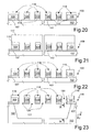
- FIGS. 19-23 show cross-sections of the wafer of FIG. 17, in successive manufacturing steps
- FIG. 24 shows a perspective cross-section of part of the wafer of FIG. 22.
- FIGS. 25-26 show cross-sections of the wafer of FIG. 23, on a reduced scale and in successive manufacture steps.
- FIGS. 1-3 show an integrated device 1 comprising a body 2 of semiconductor material, typically monocrystalline silicon, having a surface 3 and parallelepiped shape
- the body 2 is traversed by a plurality of channels 4 (visible in the sections of FIGS. 2 and 3) connected to the surface 3 of the body 2 through an inlet port 5 a and an outlet port 5 b , which are connected to the channels 4 at ends 4 a and 4 b of the channels 4 .
- Heating elements 10 are present on the surface 3 of the body 2 .
- the channels 4 extend parallel to each other, in the lengthwise direction of the body 2 , at a preset distance from the surface 3 .
- the channels 4 may have a roughly circular or rectangular section, may be spaced 50 ⁇ m, and may be set at a depth of 5-10 ⁇ m from the surface 3 .
- the channels 4 have a side of approximately 30 ⁇ 200 ⁇ m and occupy an area of 5 ⁇ 10 mm.
- the channels 4 are all connected to a same inlet port 5 a and to a same outlet port 5 b , and are thus in parallel.
- the inlet port 5 a and outlet port 5 b have an elongated shape and extend perpendicularly to the channels 4 and to the surface 3 , at the two opposite ends of the channels 4 .
- the channels 4 are spaced from each other and have respective inlet ports 12 a and respective outlet ports 12 b , which extend perpendicular to the channels 4 and to the surface 3 .
- the inlet ports 12 a are preferably aligned and connected to a first end 4 a of the channels 4
- the outlet ports 12 b are aligned and connected to a second end 4 b of the channels 4 .
- the heating elements 10 are formed, as been mentioned, on the surface 3 of the body 2 and are insulated from the body 2 by an electrically insulating material layer 17 , for example of silicon dioxide.
- Each of the heating elements 10 which are four in number in the illustrated embodiment, comprise a rectangular region that extends transversely with respect to the extension of the channels 4 , and the heating elements 10 are adjacent to each other so as to practically cover the entire portion of the surface 3 overlying the channels 4 , except for intermediate strips 11 of the surface 3 .
- Each of the heating elements 10 is connected by two electric connection regions 13 arranged on the opposite shorter sides of each of the heating elements 10 .
- sensor elements 15 extend above the intermediate strips 11 of the surface 3 , and include for example coil-shaped metal regions that are represented schematically and are connected at their ends to contact regions 16 .
- the sensing elements 15 are of a material having a resistance that varies with the temperature and are connected to a resistance sensing circuit of known type, for example of bridge type, not illustrated and preferably formed in the body 2 .
- the body 2 may integrate electronic components for controlling the temperature and/or for processing the signals picked up by the integrated device.
- the liquid to be treated and/or to be made to react with a reagent is introduced from a reservoir located above the integrated device 1 through the inlet port 5 a or the inlet ports 12 a , is forced to flow through the channels 4 , and is possibly mixed with appropriate reagents at a controlled temperature.
- the heating elements 10 maintain a controlled temperature throughout the channel area; in particular, because of its micrometric dimensions, the entire channel area 4 is evenly heated, and there is no temperature gradient along and across the channels 4 themselves.
- the treated and/or reacted liquid exits the integrated device 1 through the outlet port 5 b or the outlet ports 12 b.
- a hard mask 25 is initially formed on the surface 22 of a wafer 21 of semiconductor material, for example silicon, using processing steps known in microelectronics; the hard mask 25 comprising overlying oxide regions 23 and nitride regions 24 , which delimit between each other elongated ports extending perpendicularly to the drawing plane.
- the wafer 21 is etched (first trench etch), so as to form trenches 26 (FIG. 5) having a width, for example, of between 0.2 and 3 ⁇ m, and a depth of, for example, between 20 and 30 ⁇ m.
- the trenches 26 are preferably parallel to one another and spaced 1-30 ⁇ m.
- the wafer 21 is oxidized to form an oxide layer 27 having a thickness, for instance, of approximately 20 nm, which covers the walls 26 a and bottom 26 b of the trenches 26 and joins the oxide portions 23 , so as to form a single layer.
- a nitride layer 28 is then deposited having a thickness of between 90 and 150 nm, joining the nitride portions 24 , to form a single layer.
- the second nitride layer 28 is not indispensable.
- the nitride is dry etched and the oxide is dry or wet etched.
- the horizontal portions of the nitride layer 28 and oxide layer 27 as well as the horizontal portions of the second nitride layer 28 on the surface 3 of the wafer 21 are so removed from a bottom 26 b of the trenches 26 , so forming spacers 30 on walls 26 a of the trenches 26 and leaving the monocrystalline silicon bare on the bottom 26 b of the trenches 26 .
- the hard mask 25 remains on the surface 3 of the wafer 21 .
- silicon is etched beneath the trenches 26 for a given time using tetramethyl ammonium hydroxide (TMAH).
- TMAH tetramethyl ammonium hydroxide
- an isotropic etch may be carried out.
- the channels 4 are formed, which have a much greater width than the trenches 26 .
- the walls of the channels 4 are coated with an inhibiting layer 31 , which does not allow epitaxial growth.
- an inhibiting layer 31 which does not allow epitaxial growth.
- a fast oxidation step may be carried out, so as to grow an oxide layer (having a thickness greater than that of the oxide portions 23 and 27 that coat the surface 3 of the wafer 21 and the wall 26 a of the trenches 26 , as explained later, for example a thickness of between 60 and 100 nm), or else a layer of a material chosen among deposited oxide, nitride and tetraethyl orthosilicate (TEOS) may be deposited in a similar way.
- the inhibiting layer 31 may be dispensed with, as explained hereinbelow.
- the first spacers 30 are removed from the walls 26 a of the trenches 26 , and the hard mask 25 is removed from the surface 3 of the wafer 21 .
- the oxide portions 26 and 27 also part of the inhibiting layer 31 is removed, which, however, being thicker, as mentioned above, is not removed completely and remains to a sufficient extent to guarantee complete coverage of the walls of the channels 4 .
- an epitaxial layer 33 is grown, using the monocrystalline silicon of the wafer 21 as nucleus. Consequently, monocrystalline silicon grows horizontally inside the trenches 26 , so closing them, and vertically starting from the surface 3 (which is no longer illustrated in FIG. 11 ). If the inhibiting layer 31 is present, it inhibits growth of the silicon inside the channels 4 in such a way that the latter maintain their original dimensions determined by the timed TMAH etching. If instead, the inhibiting layer 31 is not present, the channels 4 partially close. This may be advantageous in the case where the exact dimensions of the channels 4 are not very important, and it is preferred, instead, not to have any material other than silicon on the walls of the channel 4 .
- a monolithic monocrystalline-silicon wafer 35 is obtained, including the substrate 21 and the epitaxial layer 33 , and housing completely closed channels 4 , which are delimited internally by the inhibiting layer 31 .
- conductive and/or insulating regions may be formed for manufacturing integrated electrical components belonging to control circuits and/or circuits for processing signals required for the operation of the thermoregulation device 1 .
- an insulating layer 37 for example of silicon dioxide, is formed on the surface 36 of the wafer 35 .
- the insulating layer 37 has, for example, a thickness of 200-300 nm so as to have a reduced thermal resistance.
- the inlet ports 5 a or 12 a and outlet ports 5 b or 12 b are formed (FIG. 13 ).
- the heating elements 10 are formed, for example a polycrystalline silicon layer is deposited and defined photolithographically (FIG. 14 ).
- conductive and/or insulating regions are formed as necessary for manufacturing integrated electronic components, not shown. Further steps then follow including depositing and defining metal layers to form metal connection regions 13 , the sensing elements 15 , and electric connection lines, as well as any other steps required for forming service layers. Finally, the wafer 35 is fixed to a silicon cover wafer (not shown) containing reservoirs and further elements necessary for the desired application, and the assembly is then cut into individual dice.
- a wafer 100 comprises a substrate 102 of monocrystalline semiconductor material, for example silicon, having an upper surface 103 .
- the substrate 102 has a ⁇ 110> crystallographic orientation instead of ⁇ 100>, as can be seen in FIG. 16, which also shows the flat of the wafer 100 with ⁇ 111> orientation.
- FIG. 16 also shows the longitudinal direction L of a channel 121 , which is still to be formed at this step.
- An upper stack of layers 105 is formed on the upper surface 103 and comprises a pad oxide layer 107 , of, for example, approximately 60 nm; a first nitride layer 108 , of, for example, approximately 90 nm; a polysilicon layer 109 , of, for example 450-900 nm; and a second nitride layer 110 , of, for example, 140 nm.
- the upper stack of layers 105 is masked using a resist mask 115 , which has a plurality of windows 116 , arranged according to a suitable pattern, as shown in FIG. 18 .
- the apertures 116 have a square shape, with sides inclined at 45° with respect to a longitudinal direction of the resist mask 115 , parallel to z-axis.
- the sides of the apertures 116 are approximately 2 ⁇ m, and extend at a distance of 1.4 ⁇ m from a facing side of an adjacent aperture 116 .
- the longitudinal direction z of the resist mask 115 parallel to the longitudinal direction of the buried channels to be formed in the substrate 102 , is parallel to the flat of the wafer 100 , which has an ⁇ 111> orientation, as shown in FIG. 16 .
- the second nitride layer 110 , the polysilicon layer 109 , and the first nitride layer 108 are successively etched, thus providing a hard mask 118 , formed by the remaining portions of the layers 108 - 110 , and having the same pattern as the resist mask 115 shown in FIG. 18 .
- a hard mask 118 formed by the remaining portions of the layers 108 - 110 , and having the same pattern as the resist mask 115 shown in FIG. 18 .
- the hard mask 118 is etched using TMAH (tetramethylammoniumhydroxide), such as to remove part of the uncovered polycrystalline silicon of the polysilicon layer 109 (undercut step) from the sides; a similar nitride layer is then deposited (for example with a thickness of 90 nm), which merges with the first and second nitride layers 108 , 110 .
- TMAH tetramethylammoniumhydroxide
- FIG. 20 the structure is dry etched, such as to completely remove the portions of conform nitride layer which extend immediately on top of the pad oxide layer 107 .
- the second nitride layer 110 and the polysilicon layer 109 are etched externally to the area where the channels are to be formed, using a resist mask 117 .
- the pad oxide layer is etched with 1:10 hydrofluoric acid, and is removed where it is exposed; in particular, externally to the area where the channels are to be formed, the pad oxide 107 is protected by the first nitride layer 108 .
- FIG. 23 the monocrystalline silicon of the substrate 102 is etched using TMAH, to a depth of 500-600 ⁇ m, thus forming one or more channels 121 .
- the high depth of the channels 121 which can be obtained through the described etching conditions, reduces the number of channels 121 that are necessary for processing a predetermined quantity of fluid, and thus reduces the area occupied by the channels 121 .
- a capacity of 1 ul is desired, with a length of the channels 21 in the z-direction of 10 mm, where previously it had been proposed to form twenty channels with a width of 200 ⁇ m (in x-direction) and a depth of 25 ⁇ m (in y-direction), with a total transverse dimension of approximately 5 mm in x-direction (assuming that the channels are at a distance of 50 ⁇ m from one another), it is now possible to form only two channels 121 having a width of 100 ⁇ m in x-direction, and a depth of 500 ⁇ m, with an overall transverse dimension of 0.3 mm in x-direction, the channels being arranged at a distance of 100 ⁇ m from one another, or it is possible to form a
- the covering layer 119 is removed from the front of the wafer 100 (nitride layers 108 , 110 , conform layer, and pad oxide layer 107 ); in this step, the nitride and the pad oxide layers 108 , 107 are also removed externally to the area of the channels 121 , except on the outer periphery of the channels 121 , below the polysilicon layer 109 , where they form a frame region indicated at 122 as a whole.
- an epitaxial layer 123 is grown, with a thickness, for example, of 10 ⁇ m.
- the epitaxial growth takes place both vertically and horizontally; thus a polycrystalline epitaxial portion 123 a grows on the polysilicon layer 109 , and a monocrystalline epitaxial portion 123 b grows on the substrate 102 .
- a first insulating layer 125 is formed on the epitaxial layer 123 ; preferably, the first insulating layer 125 is obtained by thermal oxidation of silicon of the epitaxial layer 123 , to a thickness of, for example, 500 nm.
- the integrated device 1 has the following advantages:
- the treatment costs are much lower than presently, since the device according to the invention enables treatment of very small amounts of fluid (i.e., in the region of microliters instead of milliliters), and it is possible to achieve better performance of the chemical reactions due to the reduced path of the reagents;
- thermoregulation device can be made in an easily reproducible way, because of the use of well-known and controllable manufacturing technologies
- the channels 4 are buried inside the semiconductor wafer 35 , they are not exposed to the external environment, even before fixing a covering element, and hence are less subject to possible contamination, for example due to subsequent manipulation and/or to the glue used for fixing the covering element;
- channels 4 having the desired shape and dimensions.
- the integrated device 1 has greatly reduced dimensions, owing to the high depth of the channels 21 , which, as previously stated, reduces the number of channels necessary per unit of volume of processed fluid.
- the manufacture requires steps that are conventional in microelectronics, with reduced costs per item; the process also has low criticality and a high productivity, and does not require the use of critical materials.
- thermoregulation device 1 may comprise a single buried channel of a suitable width, and the trenches 26 may be set at a distance whereby, in the subsequent timed TMAH etching for forming the channels 4 , the silicon between the channels 4 themselves is removed completely.
Landscapes
- Chemical & Material Sciences (AREA)
- Health & Medical Sciences (AREA)
- Engineering & Computer Science (AREA)
- Chemical Kinetics & Catalysis (AREA)
- Dispersion Chemistry (AREA)
- Mechanical Engineering (AREA)
- General Health & Medical Sciences (AREA)
- Clinical Laboratory Science (AREA)
- Life Sciences & Earth Sciences (AREA)
- Hematology (AREA)
- Analytical Chemistry (AREA)
- Molecular Biology (AREA)
- Biochemistry (AREA)
- Environmental Sciences (AREA)
- Forests & Forestry (AREA)
- Textile Engineering (AREA)
- Organic Chemistry (AREA)
- Micromachines (AREA)
- Physical Or Chemical Processes And Apparatus (AREA)
- Apparatus Associated With Microorganisms And Enzymes (AREA)
- Sampling And Sample Adjustment (AREA)
Abstract
Description
Claims (27)
Applications Claiming Priority (3)
| Application Number | Priority Date | Filing Date | Title |
|---|---|---|---|
| EP00830098 | 2000-02-11 | ||
| EP00830098.00 | 2000-02-11 | ||
| EP00830098A EP1123739B1 (en) | 2000-02-11 | 2000-02-11 | Integrated device for microfluid thermoregulation, and manufacturing process thereof |
Publications (2)
| Publication Number | Publication Date |
|---|---|
| US20010024820A1 US20010024820A1 (en) | 2001-09-27 |
| US6673593B2 true US6673593B2 (en) | 2004-01-06 |
Family
ID=8175178
Family Applications (2)
| Application Number | Title | Priority Date | Filing Date |
|---|---|---|---|
| US09/779,980 Expired - Lifetime US6673593B2 (en) | 2000-02-11 | 2001-02-08 | Integrated device for microfluid thermoregulation, and manufacturing process thereof |
| US10/706,246 Abandoned US20040096964A1 (en) | 2000-02-11 | 2003-11-12 | Integrated device for amplification and other biological tests, and manufacturing process thereof |
Family Applications After (1)
| Application Number | Title | Priority Date | Filing Date |
|---|---|---|---|
| US10/706,246 Abandoned US20040096964A1 (en) | 2000-02-11 | 2003-11-12 | Integrated device for amplification and other biological tests, and manufacturing process thereof |
Country Status (3)
| Country | Link |
|---|---|
| US (2) | US6673593B2 (en) |
| EP (1) | EP1123739B1 (en) |
| DE (1) | DE60032113T2 (en) |
Cited By (22)
| Publication number | Priority date | Publication date | Assignee | Title |
|---|---|---|---|---|
| US20030116552A1 (en) * | 2001-12-20 | 2003-06-26 | Stmicroelectronics Inc. | Heating element for microfluidic and micromechanical applications |
| US20030169799A1 (en) * | 2002-03-06 | 2003-09-11 | Dong-Il Cho | Temperature control method and apparatus for driving polymerize chain reaction (PCR) chip |
| US20040096964A1 (en) * | 2000-02-11 | 2004-05-20 | Stmicroelectronics S.R.1. | Integrated device for amplification and other biological tests, and manufacturing process thereof |
| US20040164068A1 (en) * | 2000-06-05 | 2004-08-26 | Flavio Villa | Process for manufacturing integrated chemical microreactors of semiconductor material |
| US20040206749A1 (en) * | 2001-04-23 | 2004-10-21 | Flavio Villa | Integrated device based upon semiconductor technology, in particular chemical microreactor |
| US20040226908A1 (en) * | 2000-09-27 | 2004-11-18 | Stmicroelectronics S.R.L. | Integrated chemical microreactor, thermally insulated from detection electrodes, and manufacturing and operating methods therefor |
| US20050155860A1 (en) * | 2003-12-23 | 2005-07-21 | Michele Palmieri | 03-CA-191 Microfluidic device and method of locally concentrating electrically charged substances in a microfluidic device |
| US20050161327A1 (en) * | 2003-12-23 | 2005-07-28 | Michele Palmieri | Microfluidic device and method for transporting electrically charged substances through a microchannel of a microfluidic device |
| US20050186585A1 (en) * | 2004-02-24 | 2005-08-25 | Thermal Gradient | Thermal cycling device |
| US20070190685A1 (en) * | 2006-02-10 | 2007-08-16 | Ralph Ebbutt | Cooling facility and method for integrated circuit |
| US20070202531A1 (en) * | 2004-02-24 | 2007-08-30 | Joel Grover | Thermal Cycling Device |
| US20090060795A1 (en) * | 2007-08-29 | 2009-03-05 | Canon U.S. Life Sciences, Inc. | Microfluidic devices with integrated resistive heater electrodes including systems and methods for controlling and measuring the temperatures of such heater electrodes |
| US20090215194A1 (en) * | 2006-06-23 | 2009-08-27 | Stmicroelectronics, S.R.L | Assembly of a microfluidic device for analysis of biological material |
| US20090214391A1 (en) * | 2005-05-12 | 2009-08-27 | Stmicroeletronics S.R.L. | Microfluidic Device With Integrated Micropump, In Particular Biochemical Microreactor, And Manufacturing Method Thereof |
| US20100213373A1 (en) * | 2009-02-26 | 2010-08-26 | Texas Instruments Incorporated | Infrared sensor structure and method |
| US20100327393A1 (en) * | 2009-06-24 | 2010-12-30 | Texas Instruments Incorporated | Method and structures for etching cavity in silicon under dielectric membrane |
| EP2339320A1 (en) | 2005-01-25 | 2011-06-29 | Oscillogy LLC | Temperature controller for small fluid samples having different heat capacities |
| US20120040856A1 (en) * | 2008-12-23 | 2012-02-16 | Stmicroelectronics S.R.L. | Method for detecting the presence of liquids in a microfluidic device, detecting apparatus and corresponding microfluidic device |
| US8727504B2 (en) | 2011-11-11 | 2014-05-20 | Stmicroelectronics, Inc. | Microfluidic jetting device with piezoelectric actuator and method for making the same |
| US8956325B2 (en) | 2011-12-07 | 2015-02-17 | Stmicroelectronics, Inc. | Piezoelectric microfluidic pumping device and method for using the same |
| USD879321S1 (en) * | 2018-11-02 | 2020-03-24 | Group K Diagnostics, Inc. | Microfluidic device |
| US11642669B2 (en) | 2017-10-18 | 2023-05-09 | Group K Diagnostics, Inc. | Single-layer microfluidic device and methods of manufacture and use thereof |
Families Citing this family (60)
| Publication number | Priority date | Publication date | Assignee | Title |
|---|---|---|---|---|
| US7452713B2 (en) | 2000-02-29 | 2008-11-18 | Stmicroelectronics S.R.L. | Process for manufacturing a microfluidic device with buried channels |
| US6544477B1 (en) | 2000-08-01 | 2003-04-08 | Regents Of The University Of Minnesota | Apparatus for generating a temperature gradient |
| US6387791B1 (en) * | 2000-12-14 | 2002-05-14 | Bae Systems, Information And Electronic Systems Integration, Inc. | Method for manufacturing microscopic canals within a semiconductor |
| US6714102B2 (en) * | 2001-03-01 | 2004-03-30 | Agilent Technologies, Inc. | Method of fabricating thin film bulk acoustic resonator (FBAR) and FBAR structure embodying the method |
| US20050130297A1 (en) * | 2001-04-26 | 2005-06-16 | Societe Nouvelle Cell Tissue Progress | Cell and tissue culture device with temperature regulation |
| DE10146545A1 (en) * | 2001-09-21 | 2003-04-10 | Merck Patent Gmbh | microcomponent |
| US6942018B2 (en) | 2001-09-28 | 2005-09-13 | The Board Of Trustees Of The Leland Stanford Junior University | Electroosmotic microchannel cooling system |
| US7134486B2 (en) | 2001-09-28 | 2006-11-14 | The Board Of Trustees Of The Leeland Stanford Junior University | Control of electrolysis gases in electroosmotic pump systems |
| DE10204414A1 (en) | 2002-02-04 | 2003-09-04 | Siemens Ag | Microfluidic system |
| US6606251B1 (en) | 2002-02-07 | 2003-08-12 | Cooligy Inc. | Power conditioning module |
| ITTO20020809A1 (en) | 2002-09-17 | 2004-03-18 | St Microelectronics Srl | MICROPUMP, IN PARTICULAR FOR AN INTEGRATED DNA ANALYSIS DEVICE. |
| US6881039B2 (en) | 2002-09-23 | 2005-04-19 | Cooligy, Inc. | Micro-fabricated electrokinetic pump |
| AU2003270882A1 (en) | 2002-09-23 | 2004-05-04 | Cooligy, Inc. | Micro-fabricated electrokinetic pump with on-frit electrode |
| US6994151B2 (en) | 2002-10-22 | 2006-02-07 | Cooligy, Inc. | Vapor escape microchannel heat exchanger |
| US20040076408A1 (en) * | 2002-10-22 | 2004-04-22 | Cooligy Inc. | Method and apparatus for removeably coupling a heat rejection device with a heat producing device |
| US7836597B2 (en) | 2002-11-01 | 2010-11-23 | Cooligy Inc. | Method of fabricating high surface to volume ratio structures and their integration in microheat exchangers for liquid cooling system |
| TWI300466B (en) | 2002-11-01 | 2008-09-01 | Cooligy Inc | Channeled flat plate fin heat exchange system, device and method |
| US7156159B2 (en) | 2003-03-17 | 2007-01-02 | Cooligy, Inc. | Multi-level microchannel heat exchangers |
| US7000684B2 (en) | 2002-11-01 | 2006-02-21 | Cooligy, Inc. | Method and apparatus for efficient vertical fluid delivery for cooling a heat producing device |
| WO2004042306A2 (en) | 2002-11-01 | 2004-05-21 | Cooligy, Inc. | Method and apparatus for achieving temperature uniformity and hot spot cooling in a heat producing device |
| US6986382B2 (en) | 2002-11-01 | 2006-01-17 | Cooligy Inc. | Interwoven manifolds for pressure drop reduction in microchannel heat exchangers |
| US7293423B2 (en) | 2004-06-04 | 2007-11-13 | Cooligy Inc. | Method and apparatus for controlling freezing nucleation and propagation |
| US7201012B2 (en) | 2003-01-31 | 2007-04-10 | Cooligy, Inc. | Remedies to prevent cracking in a liquid system |
| US7044196B2 (en) | 2003-01-31 | 2006-05-16 | Cooligy,Inc | Decoupled spring-loaded mounting apparatus and method of manufacturing thereof |
| US7090001B2 (en) | 2003-01-31 | 2006-08-15 | Cooligy, Inc. | Optimized multiple heat pipe blocks for electronics cooling |
| US7017654B2 (en) | 2003-03-17 | 2006-03-28 | Cooligy, Inc. | Apparatus and method of forming channels in a heat-exchanging device |
| US7591302B1 (en) | 2003-07-23 | 2009-09-22 | Cooligy Inc. | Pump and fan control concepts in a cooling system |
| US7021369B2 (en) * | 2003-07-23 | 2006-04-04 | Cooligy, Inc. | Hermetic closed loop fluid system |
| EP1541991A1 (en) | 2003-12-12 | 2005-06-15 | STMicroelectronics S.r.l. | Integrated semiconductor chemical microreactor for real-time monitoring of biological reactions |
| US7188662B2 (en) | 2004-06-04 | 2007-03-13 | Cooligy, Inc. | Apparatus and method of efficient fluid delivery for cooling a heat producing device |
| US7616444B2 (en) | 2004-06-04 | 2009-11-10 | Cooligy Inc. | Gimballed attachment for multiple heat exchangers |
| US20060001039A1 (en) * | 2004-06-30 | 2006-01-05 | Stmicroelectronics, Inc. | Method of forming buried channels and microfluidic devices having the same |
| EP1618955B1 (en) | 2004-07-19 | 2010-12-22 | STMicroelectronics Srl | Biological molecules detection device having increased detection rate, and method for quick detection of biological molecules |
| US7913719B2 (en) | 2006-01-30 | 2011-03-29 | Cooligy Inc. | Tape-wrapped multilayer tubing and methods for making the same |
| US8157001B2 (en) | 2006-03-30 | 2012-04-17 | Cooligy Inc. | Integrated liquid to air conduction module |
| US7715194B2 (en) | 2006-04-11 | 2010-05-11 | Cooligy Inc. | Methodology of cooling multiple heat sources in a personal computer through the use of multiple fluid-based heat exchanging loops coupled via modular bus-type heat exchangers |
| EP1878503A1 (en) * | 2006-07-14 | 2008-01-16 | Roche Diagnostics GmbH | Temperature sensor element for monitoring heating and cooling |
| EP1878502A1 (en) | 2006-07-14 | 2008-01-16 | Roche Diagnostics GmbH | Instrument for heating and cooling |
| EP1878501A1 (en) | 2006-07-14 | 2008-01-16 | Roche Diagnostics GmbH | Instrument for heating and cooling |
| TW200924625A (en) | 2007-08-07 | 2009-06-01 | Cooligy Inc | Deformable duct guides that accommodate electronic connection lines |
| US9297571B1 (en) | 2008-03-10 | 2016-03-29 | Liebert Corporation | Device and methodology for the removal of heat from an equipment rack by means of heat exchangers mounted to a door |
| US20090225514A1 (en) | 2008-03-10 | 2009-09-10 | Adrian Correa | Device and methodology for the removal of heat from an equipment rack by means of heat exchangers mounted to a door |
| WO2009151407A2 (en) | 2008-06-14 | 2009-12-17 | Veredus Laboratories Pte Ltd | Influenza sequences |
| US8369070B2 (en) | 2010-01-13 | 2013-02-05 | The Aerospace Corporation | Photostructured electronic devices and methods for making same |
| US9146377B2 (en) | 2010-01-13 | 2015-09-29 | The Aerospace Corporation | Photostructured optical devices and methods for making same |
| US8410660B2 (en) | 2010-01-13 | 2013-04-02 | The Aerospace Corporation | Acoustic devices embedded in photostructurable ceramics |
| US8479375B2 (en) * | 2010-01-13 | 2013-07-09 | The Aerospace Corporation | Method of making an embedded electromagnetic device |
| US8940241B2 (en) | 2010-01-13 | 2015-01-27 | The Aerospace Corporation | Photostructured chemical devices and methods for making same |
| US8455242B2 (en) | 2010-02-22 | 2013-06-04 | Hyclone Laboratories, Inc. | Mixing system with condenser |
| US8633553B2 (en) * | 2010-07-26 | 2014-01-21 | Stmicroelectronics S.R.L. | Process for manufacturing a micromechanical structure having a buried area provided with a filter |
| US9061382B2 (en) * | 2011-07-25 | 2015-06-23 | International Business Machines Corporation | Heat sink structure with a vapor-permeable membrane for two-phase cooling |
| EP3466509B1 (en) | 2014-03-21 | 2021-03-10 | Life Technologies Corporation | Condenser systems for fluid processing systems |
| JP6585616B2 (en) | 2014-03-21 | 2019-10-02 | ライフ テクノロジーズ コーポレイション | Gas filter system for fluid treatment system |
| US9457306B2 (en) | 2014-10-07 | 2016-10-04 | Life Technologies Corporation | Regulated vacuum off-gassing of gas filter for fluid processing system and related methods |
| KR20160104422A (en) | 2015-02-26 | 2016-09-05 | 한국전자통신연구원 | Method for constructing a system for controlling and managing hierarchical and multi-virtual network based applications and services |
| CN108778515B (en) | 2015-12-29 | 2020-11-17 | 生命科技股份有限公司 | Flexible bioprocessing container with partially partitioned compartments |
| IT201700034134A1 (en) | 2017-03-28 | 2018-09-28 | St Microelectronics Srl | FLUID-RELEASE DEVICE WITH CROSSTALK REDUCTION ELEMENT, PRINT HEAD INCLUDING THE EJECTION DEVICE, PRINTER INCLUDING THE PRINT HEAD AND PROCESS OF MANUFACTURING THE EJECTION DEVICE |
| EP3546931B1 (en) * | 2018-03-28 | 2021-07-21 | Siemens Aktiengesellschaft | Thermoresistive gas sensor, flow sensor and thermal conductivity sensor |
| GB201812192D0 (en) | 2018-07-26 | 2018-09-12 | Ttp Plc | Variable temperature reactor, heater and control circuit for the same |
| EP3671195B1 (en) * | 2018-12-17 | 2025-02-12 | Siemens Aktiengesellschaft | Thermoresistive gas sensor |
Citations (9)
| Publication number | Priority date | Publication date | Assignee | Title |
|---|---|---|---|---|
| US5429734A (en) | 1993-10-12 | 1995-07-04 | Massachusetts Institute Of Technology | Monolithic capillary electrophoretic device |
| US5639423A (en) * | 1992-08-31 | 1997-06-17 | The Regents Of The University Of Calfornia | Microfabricated reactor |
| US5690841A (en) | 1993-12-10 | 1997-11-25 | Pharmacia Biotech Ab | Method of producing cavity structures |
| GB2325464A (en) | 1997-04-23 | 1998-11-25 | Bruker Franzen Analytik Gmbh | Capillary polymerase chain reaction |
| US5858195A (en) | 1994-08-01 | 1999-01-12 | Lockheed Martin Energy Research Corporation | Apparatus and method for performing microfluidic manipulations for chemical analysis and synthesis |
| US6319469B1 (en) * | 1995-12-18 | 2001-11-20 | Silicon Valley Bank | Devices and methods for using centripetal acceleration to drive fluid movement in a microfluidics system |
| US6368871B1 (en) * | 1997-08-13 | 2002-04-09 | Cepheid | Non-planar microstructures for manipulation of fluid samples |
| US6403367B1 (en) * | 1994-07-07 | 2002-06-11 | Nanogen, Inc. | Integrated portable biological detection system |
| US6440725B1 (en) * | 1997-12-24 | 2002-08-27 | Cepheid | Integrated fluid manipulation cartridge |
Family Cites Families (22)
| Publication number | Priority date | Publication date | Assignee | Title |
|---|---|---|---|---|
| US4993143A (en) * | 1989-03-06 | 1991-02-19 | Delco Electronics Corporation | Method of making a semiconductive structure useful as a pressure sensor |
| US6051380A (en) * | 1993-11-01 | 2000-04-18 | Nanogen, Inc. | Methods and procedures for molecular biological analysis and diagnostics |
| US5637469A (en) * | 1992-05-01 | 1997-06-10 | Trustees Of The University Of Pennsylvania | Methods and apparatus for the detection of an analyte utilizing mesoscale flow systems |
| DE4435107C1 (en) * | 1994-09-30 | 1996-04-04 | Biometra Biomedizinische Analy | Miniaturized flow thermal cycler |
| DE19519015C1 (en) * | 1995-05-24 | 1996-09-05 | Inst Physikalische Hochtech Ev | Miniaturised multi-chamber thermo-cycler for polymerase chain reaction |
| US6168948B1 (en) * | 1995-06-29 | 2001-01-02 | Affymetrix, Inc. | Miniaturized genetic analysis systems and methods |
| US5856174A (en) * | 1995-06-29 | 1999-01-05 | Affymetrix, Inc. | Integrated nucleic acid diagnostic device |
| US20020068357A1 (en) * | 1995-09-28 | 2002-06-06 | Mathies Richard A. | Miniaturized integrated nucleic acid processing and analysis device and method |
| US5942443A (en) * | 1996-06-28 | 1999-08-24 | Caliper Technologies Corporation | High throughput screening assay systems in microscale fluidic devices |
| CN1173776C (en) * | 1996-06-28 | 2004-11-03 | 卡钳技术有限公司 | High Throughput Screening Analysis System in Microscale Fluidic Devices |
| US5942449A (en) * | 1996-08-28 | 1999-08-24 | Micron Technology, Inc. | Method for removing an upper layer of material from a semiconductor wafer |
| US6031286A (en) * | 1997-02-28 | 2000-02-29 | International Business Machines Corporation | Semiconductor structures containing a micro pipe system therein |
| US6261431B1 (en) * | 1998-12-28 | 2001-07-17 | Affymetrix, Inc. | Process for microfabrication of an integrated PCR-CE device and products produced by the same |
| US6238868B1 (en) * | 1999-04-12 | 2001-05-29 | Nanogen/Becton Dickinson Partnership | Multiplex amplification and separation of nucleic acid sequences using ligation-dependant strand displacement amplification and bioelectronic chip technology |
| DE69935495T2 (en) * | 1999-04-29 | 2007-11-29 | Stmicroelectronics S.R.L., Agrate Brianza | Manufacturing process for buried channels and cavities in semiconductor wafers |
| US6878540B2 (en) * | 1999-06-25 | 2005-04-12 | Cepheid | Device for lysing cells, spores, or microorganisms |
| US6258263B1 (en) * | 1999-09-17 | 2001-07-10 | The University Of Cincinnati | Liquid chromatograph on a chip |
| EP1123739B1 (en) * | 2000-02-11 | 2006-11-29 | STMicroelectronics S.r.l. | Integrated device for microfluid thermoregulation, and manufacturing process thereof |
| DE60023464T2 (en) * | 2000-06-05 | 2006-07-20 | Stmicroelectronics S.R.L., Agrate Brianza | Process for the production of integrated chemical microreactors made of semiconductor material and integrated microreactor |
| EP1182602B1 (en) * | 2000-08-25 | 2007-04-25 | STMicroelectronics S.r.l. | A system for the automatic analysis of DNA microarray images |
| DE60032772T2 (en) * | 2000-09-27 | 2007-11-08 | Stmicroelectronics S.R.L., Agrate Brianza | Integrated chemical microreactor with thermally insulated measuring electrodes and method for its production |
| US6727479B2 (en) * | 2001-04-23 | 2004-04-27 | Stmicroelectronics S.R.L. | Integrated device based upon semiconductor technology, in particular chemical microreactor |
-
2000
- 2000-02-11 EP EP00830098A patent/EP1123739B1/en not_active Expired - Lifetime
- 2000-02-11 DE DE60032113T patent/DE60032113T2/en not_active Expired - Lifetime
-
2001
- 2001-02-08 US US09/779,980 patent/US6673593B2/en not_active Expired - Lifetime
-
2003
- 2003-11-12 US US10/706,246 patent/US20040096964A1/en not_active Abandoned
Patent Citations (12)
| Publication number | Priority date | Publication date | Assignee | Title |
|---|---|---|---|---|
| US5639423A (en) * | 1992-08-31 | 1997-06-17 | The Regents Of The University Of Calfornia | Microfabricated reactor |
| US5429734A (en) | 1993-10-12 | 1995-07-04 | Massachusetts Institute Of Technology | Monolithic capillary electrophoretic device |
| US5690841A (en) | 1993-12-10 | 1997-11-25 | Pharmacia Biotech Ab | Method of producing cavity structures |
| US6403367B1 (en) * | 1994-07-07 | 2002-06-11 | Nanogen, Inc. | Integrated portable biological detection system |
| US5858195A (en) | 1994-08-01 | 1999-01-12 | Lockheed Martin Energy Research Corporation | Apparatus and method for performing microfluidic manipulations for chemical analysis and synthesis |
| US6001229A (en) | 1994-08-01 | 1999-12-14 | Lockheed Martin Energy Systems, Inc. | Apparatus and method for performing microfluidic manipulations for chemical analysis |
| US6010607A (en) | 1994-08-01 | 2000-01-04 | Lockheed Martin Energy Research Corporation | Apparatus and method for performing microfluidic manipulations for chemical analysis and synthesis |
| US6010608A (en) | 1994-08-01 | 2000-01-04 | Lockheed Martin Energy Research Corporation | Apparatus and method for performing microfluidic manipulations for chemical analysis and synthesis |
| US6319469B1 (en) * | 1995-12-18 | 2001-11-20 | Silicon Valley Bank | Devices and methods for using centripetal acceleration to drive fluid movement in a microfluidics system |
| GB2325464A (en) | 1997-04-23 | 1998-11-25 | Bruker Franzen Analytik Gmbh | Capillary polymerase chain reaction |
| US6368871B1 (en) * | 1997-08-13 | 2002-04-09 | Cepheid | Non-planar microstructures for manipulation of fluid samples |
| US6440725B1 (en) * | 1997-12-24 | 2002-08-27 | Cepheid | Integrated fluid manipulation cartridge |
Non-Patent Citations (1)
| Title |
|---|
| Kopp, Martin U. et al., "Chemical Amplification: Continous-Flow PCR on a Chip," Science, vol. 280, pp. 1046-1048: May 15, 1998. |
Cited By (42)
| Publication number | Priority date | Publication date | Assignee | Title |
|---|---|---|---|---|
| US20040096964A1 (en) * | 2000-02-11 | 2004-05-20 | Stmicroelectronics S.R.1. | Integrated device for amplification and other biological tests, and manufacturing process thereof |
| US20040164068A1 (en) * | 2000-06-05 | 2004-08-26 | Flavio Villa | Process for manufacturing integrated chemical microreactors of semiconductor material |
| US7009154B2 (en) * | 2000-06-05 | 2006-03-07 | Stmicroelectronics S.R.L. | Process for manufacturing integrated chemical microreactors of semiconductor material |
| US6974693B2 (en) | 2000-09-27 | 2005-12-13 | Stmicroelectronics S.R.L. | Integrated chemical microreactor, thermally insulated from detection electrodes, and manufacturing and operating methods therefor |
| US20040226908A1 (en) * | 2000-09-27 | 2004-11-18 | Stmicroelectronics S.R.L. | Integrated chemical microreactor, thermally insulated from detection electrodes, and manufacturing and operating methods therefor |
| US20040235149A1 (en) * | 2000-09-27 | 2004-11-25 | Stmicroelectronics S.R.I. | Integrated chemical microreactor, thermally insulated from detection electrodes, and manufacturing and operating methods therefor |
| US6929968B2 (en) | 2000-09-27 | 2005-08-16 | Stmicroelectronics S.R.L. | Integrated chemical microreactor, thermally insulated from detection electrodes, and manufacturing and operating methods therefor |
| US20040206749A1 (en) * | 2001-04-23 | 2004-10-21 | Flavio Villa | Integrated device based upon semiconductor technology, in particular chemical microreactor |
| US6909073B2 (en) * | 2001-04-23 | 2005-06-21 | Stmicroelectronics S.R.L. | Integrated device based upon semiconductor technology, in particular chemical microreactor |
| US20030116552A1 (en) * | 2001-12-20 | 2003-06-26 | Stmicroelectronics Inc. | Heating element for microfluidic and micromechanical applications |
| US9012810B2 (en) | 2001-12-20 | 2015-04-21 | Stmicroelectronics, Inc. | Heating element for microfluidic and micromechanical applications |
| US20070284360A1 (en) * | 2001-12-20 | 2007-12-13 | Stmicroelectronics Inc. | Heating element for microfluidic and micromechanical applications |
| US7060948B2 (en) * | 2002-03-06 | 2006-06-13 | Samsung Electronics Co., Ltd. | Temperature control method and apparatus for driving polymerase chain reaction (PCR) chip |
| US20030169799A1 (en) * | 2002-03-06 | 2003-09-11 | Dong-Il Cho | Temperature control method and apparatus for driving polymerize chain reaction (PCR) chip |
| US7485214B2 (en) | 2003-12-23 | 2009-02-03 | Stmicroelectronics S. R. L. | Microfluidic device and method of locally concentrating electrically charged substances in a microfluidic device |
| US20050161327A1 (en) * | 2003-12-23 | 2005-07-28 | Michele Palmieri | Microfluidic device and method for transporting electrically charged substances through a microchannel of a microfluidic device |
| US20050155860A1 (en) * | 2003-12-23 | 2005-07-21 | Michele Palmieri | 03-CA-191 Microfluidic device and method of locally concentrating electrically charged substances in a microfluidic device |
| US20070202531A1 (en) * | 2004-02-24 | 2007-08-30 | Joel Grover | Thermal Cycling Device |
| US20050186585A1 (en) * | 2004-02-24 | 2005-08-25 | Thermal Gradient | Thermal cycling device |
| US7618811B2 (en) | 2004-02-24 | 2009-11-17 | Thermal Gradient | Thermal cycling device |
| US8043849B2 (en) | 2004-02-24 | 2011-10-25 | Thermal Gradient | Thermal cycling device |
| EP2339320A1 (en) | 2005-01-25 | 2011-06-29 | Oscillogy LLC | Temperature controller for small fluid samples having different heat capacities |
| US20090214391A1 (en) * | 2005-05-12 | 2009-08-27 | Stmicroeletronics S.R.L. | Microfluidic Device With Integrated Micropump, In Particular Biochemical Microreactor, And Manufacturing Method Thereof |
| US8097222B2 (en) | 2005-05-12 | 2012-01-17 | Stmicroelectronics, S.R.L. | Microfluidic device with integrated micropump, in particular biochemical microreactor, and manufacturing method thereof |
| US20070190685A1 (en) * | 2006-02-10 | 2007-08-16 | Ralph Ebbutt | Cooling facility and method for integrated circuit |
| US20090215194A1 (en) * | 2006-06-23 | 2009-08-27 | Stmicroelectronics, S.R.L | Assembly of a microfluidic device for analysis of biological material |
| US8808641B2 (en) | 2006-06-23 | 2014-08-19 | Stmicroelectronics S.R.L. | Assembly of a microfluidic device for analysis of biological material |
| US9221056B2 (en) | 2007-08-29 | 2015-12-29 | Canon U.S. Life Sciences, Inc. | Microfluidic devices with integrated resistive heater electrodes including systems and methods for controlling and measuring the temperatures of such heater electrodes |
| US9823135B2 (en) | 2007-08-29 | 2017-11-21 | Canon U.S. Life Sciences, Inc. | Microfluidic devices with integrated resistive heater electrodes including systems and methods for controlling and measuring the temperatures of such heater electrodes |
| US20090060795A1 (en) * | 2007-08-29 | 2009-03-05 | Canon U.S. Life Sciences, Inc. | Microfluidic devices with integrated resistive heater electrodes including systems and methods for controlling and measuring the temperatures of such heater electrodes |
| US20120040856A1 (en) * | 2008-12-23 | 2012-02-16 | Stmicroelectronics S.R.L. | Method for detecting the presence of liquids in a microfluidic device, detecting apparatus and corresponding microfluidic device |
| US20100213373A1 (en) * | 2009-02-26 | 2010-08-26 | Texas Instruments Incorporated | Infrared sensor structure and method |
| US8604435B2 (en) | 2009-02-26 | 2013-12-10 | Texas Instruments Incorporated | Infrared sensor structure and method |
| US9417133B2 (en) | 2009-02-26 | 2016-08-16 | Texas Instruments Incorporated | Infrared sensor structure and method |
| US9157807B2 (en) * | 2009-06-24 | 2015-10-13 | Texas Instruments Incorporated | Etching cavity structures in silicon under dielectric membrane |
| US20100327393A1 (en) * | 2009-06-24 | 2010-12-30 | Texas Instruments Incorporated | Method and structures for etching cavity in silicon under dielectric membrane |
| US9427961B2 (en) | 2011-11-11 | 2016-08-30 | Stmicroelectronics, Inc. | Microfluidic jetting device with piezoelectric actuator and method for making the same |
| US8727504B2 (en) | 2011-11-11 | 2014-05-20 | Stmicroelectronics, Inc. | Microfluidic jetting device with piezoelectric actuator and method for making the same |
| US8956325B2 (en) | 2011-12-07 | 2015-02-17 | Stmicroelectronics, Inc. | Piezoelectric microfluidic pumping device and method for using the same |
| US11642669B2 (en) | 2017-10-18 | 2023-05-09 | Group K Diagnostics, Inc. | Single-layer microfluidic device and methods of manufacture and use thereof |
| USD879321S1 (en) * | 2018-11-02 | 2020-03-24 | Group K Diagnostics, Inc. | Microfluidic device |
| USD879999S1 (en) | 2018-11-02 | 2020-03-31 | Group K Diagnostics, Inc. | Microfluidic device |
Also Published As
| Publication number | Publication date |
|---|---|
| US20010024820A1 (en) | 2001-09-27 |
| EP1123739A1 (en) | 2001-08-16 |
| DE60032113T2 (en) | 2007-06-28 |
| EP1123739B1 (en) | 2006-11-29 |
| US20040096964A1 (en) | 2004-05-20 |
| DE60032113D1 (en) | 2007-01-11 |
Similar Documents
| Publication | Publication Date | Title |
|---|---|---|
| US6673593B2 (en) | Integrated device for microfluid thermoregulation, and manufacturing process thereof | |
| EP1161985B1 (en) | Process for manufacturing integrated chemical microreactors of semiconductor material, and integrated microreactor | |
| US6974693B2 (en) | Integrated chemical microreactor, thermally insulated from detection electrodes, and manufacturing and operating methods therefor | |
| US6909073B2 (en) | Integrated device based upon semiconductor technology, in particular chemical microreactor | |
| Lee et al. | Bulk-micromachined submicroliter-volume PCR chip with very rapid thermal response and low power consumption | |
| US20020173032A1 (en) | Miniaturized thermal cycler | |
| US20040132059A1 (en) | Integrated device for biological analyses | |
| EP2163306A1 (en) | Multi-well plate with tailored chambers | |
| US20060001039A1 (en) | Method of forming buried channels and microfluidic devices having the same | |
| US6680193B1 (en) | Device for chemical and/or biological analysis with analysis support | |
| CA2371767C (en) | Micro-chip for chemical reaction | |
| CN114364785A (en) | Temperature control for digital microfluidic devices | |
| KR100452946B1 (en) | Low Power Consumption Microfabricated Thermal Cycler and its Fabrication Method | |
| JP4351171B2 (en) | SAMPLE PROCESSING APPARATUS HAVING PROCESS CHAMBER WITH BYPASS SLOT AND METHOD FOR PROCESSING SAMPLE MATERIAL IN PROCESS CHAMBER | |
| Zou et al. | Miniaturized independently controllable multichamber thermal cycler | |
| US7732192B2 (en) | Integrated chemical microreactor with large area channels and manufacturing process thereof | |
| US7230315B2 (en) | Integrated chemical microreactor with large area channels and manufacturing process thereof | |
| EP1535878A1 (en) | Integrated chemical microreactor with large area channels and manufacturing process thereof | |
| KR20050003944A (en) | Fabrication method and the micro chamber structure with integrated heater and temperature sensor | |
| HK40067788A (en) | Temperature control on digital microfluidics device | |
| ITTO20010392A1 (en) | INTEGRATED DEVICE BASED ON SEMICONDUCTOR TECHNOLOGY, IN PARTICULAR CHEMICAL MICROREACTOR. |
Legal Events
| Date | Code | Title | Description |
|---|---|---|---|
| AS | Assignment |
Owner name: STMIRCROELECTRONICS S.R.L., ITALY Free format text: ASSIGNMENT OF ASSIGNORS INTEREST;ASSIGNORS:MASTROMATTEO, UBALDO;VILLA, FLAVIO;BARLOCCHI, GABRIELE;REEL/FRAME:011766/0716 Effective date: 20010403 |
|
| FEPP | Fee payment procedure |
Free format text: PAYOR NUMBER ASSIGNED (ORIGINAL EVENT CODE: ASPN); ENTITY STATUS OF PATENT OWNER: LARGE ENTITY |
|
| STCF | Information on status: patent grant |
Free format text: PATENTED CASE |
|
| FEPP | Fee payment procedure |
Free format text: PAYER NUMBER DE-ASSIGNED (ORIGINAL EVENT CODE: RMPN); ENTITY STATUS OF PATENT OWNER: LARGE ENTITY Free format text: PAYOR NUMBER ASSIGNED (ORIGINAL EVENT CODE: ASPN); ENTITY STATUS OF PATENT OWNER: LARGE ENTITY |
|
| FPAY | Fee payment |
Year of fee payment: 4 |
|
| FPAY | Fee payment |
Year of fee payment: 8 |
|
| FPAY | Fee payment |
Year of fee payment: 12 |