US6672880B2 - Laminated socket contacts - Google Patents
Laminated socket contacts Download PDFInfo
- Publication number
- US6672880B2 US6672880B2 US10/325,213 US32521302A US6672880B2 US 6672880 B2 US6672880 B2 US 6672880B2 US 32521302 A US32521302 A US 32521302A US 6672880 B2 US6672880 B2 US 6672880B2
- Authority
- US
- United States
- Prior art keywords
- panel
- conductive
- power
- ground
- socket
- Prior art date
- Legal status (The legal status is an assumption and is not a legal conclusion. Google has not performed a legal analysis and makes no representation as to the accuracy of the status listed.)
- Expired - Fee Related, expires
Links
Images


Classifications
-
- H—ELECTRICITY
- H05—ELECTRIC TECHNIQUES NOT OTHERWISE PROVIDED FOR
- H05K—PRINTED CIRCUITS; CASINGS OR CONSTRUCTIONAL DETAILS OF ELECTRIC APPARATUS; MANUFACTURE OF ASSEMBLAGES OF ELECTRICAL COMPONENTS
- H05K7/00—Constructional details common to different types of electric apparatus
- H05K7/02—Arrangements of circuit components or wiring on supporting structure
- H05K7/10—Plug-in assemblages of components, e.g. IC sockets
- H05K7/1092—Plug-in assemblages of components, e.g. IC sockets with built-in components, e.g. intelligent sockets
-
- H—ELECTRICITY
- H01—ELECTRIC ELEMENTS
- H01L—SEMICONDUCTOR DEVICES NOT COVERED BY CLASS H10
- H01L2224/00—Indexing scheme for arrangements for connecting or disconnecting semiconductor or solid-state bodies and methods related thereto as covered by H01L24/00
- H01L2224/01—Means for bonding being attached to, or being formed on, the surface to be connected, e.g. chip-to-package, die-attach, "first-level" interconnects; Manufacturing methods related thereto
- H01L2224/10—Bump connectors; Manufacturing methods related thereto
- H01L2224/15—Structure, shape, material or disposition of the bump connectors after the connecting process
- H01L2224/16—Structure, shape, material or disposition of the bump connectors after the connecting process of an individual bump connector
- H01L2224/161—Disposition
- H01L2224/16151—Disposition the bump connector connecting between a semiconductor or solid-state body and an item not being a semiconductor or solid-state body, e.g. chip-to-substrate, chip-to-passive
- H01L2224/16221—Disposition the bump connector connecting between a semiconductor or solid-state body and an item not being a semiconductor or solid-state body, e.g. chip-to-substrate, chip-to-passive the body and the item being stacked
- H01L2224/16225—Disposition the bump connector connecting between a semiconductor or solid-state body and an item not being a semiconductor or solid-state body, e.g. chip-to-substrate, chip-to-passive the body and the item being stacked the item being non-metallic, e.g. insulating substrate with or without metallisation
-
- H—ELECTRICITY
- H05—ELECTRIC TECHNIQUES NOT OTHERWISE PROVIDED FOR
- H05K—PRINTED CIRCUITS; CASINGS OR CONSTRUCTIONAL DETAILS OF ELECTRIC APPARATUS; MANUFACTURE OF ASSEMBLAGES OF ELECTRICAL COMPONENTS
- H05K1/00—Printed circuits
- H05K1/02—Details
- H05K1/0213—Electrical arrangements not otherwise provided for
- H05K1/0263—High current adaptations, e.g. printed high current conductors or using auxiliary non-printed means; Fine and coarse circuit patterns on one circuit board
Definitions
- the invention relates generally to the field of integrated circuit socket design. More particularly, the invention relates to a laminated socket contact that reduces the inductance of the package/sockets by reducing the distance between power and ground conductors of the contact.
- Improvements to the various types of sockets used to mount integrated circuit packages have focused on reducing the amount of electrical resistance presented by the contacts within the sockets.
- Various improvements have focused on increasing the contact area and/or the contact pressure in order to provide low resistance connections.
- FIG. 1 is a high level illustration of a typical socket and integrated circuit package
- FIG. 2 is a high level illustration of a socket and integrated circuit package having a power bar
- FIGS. 3 a and 3 b illustrate an integrated circuit package having a power bar
- FIG. 4 illustrates a socket for mounting an integrated circuit with a power bar
- FIG. 5 illustrates how an integrated circuit package with a power bar may be mounted in a socket
- FIG. 6 a is a top view of an integrated circuit package with side terminal connections
- FIG. 6 b is a side view of an integrated circuit package with side terminal connections
- FIG. 6 c is an alternative top view of an integrated circuit package with side terminals connections
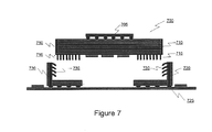
- FIG. 7 is a side view illustrating how an integrated circuit package with side terminals may be mounted in a socket
- FIG. 8 is a side view illustrating a laminated socket contacting with a power bar according to one embodiment of the present invention.
- FIG. 9 is a top view illustrating a laminated socket contacting with a power bar according to one embodiment of the present invention.
- FIG. 10 is a side view illustrating a laminated socket contact with terminals for connecting to an integrated circuit package with side terminal connections according to one embodiment of the present invention.
- FIG. 11 is a top view illustrating a laminated socket contact connecting with an integrated circuit package having side terminal connections according to one embodiment of the present inventions.
- a laminated socket contact is described for reducing inductance in power connections to an integrated circuit package.
- embodiments of the present invention seek to provide a more efficient power socket by reducing the distance between the power and ground contacts.
- the contact consists of a conductive power panel, a conductive ground panel, a thin non-conductive layer interposed between the power panel and ground panel layer, and at least one conductive finger extending from each of the power panel and ground panel.
- this socket contact may be used with power bar connectors, side terminal connectors or pin connectors.
- FIG. 1 is a high level illustration of a typical socket and integrated circuit package.
- This example illustrates an integrated circuit package 111 having a number of pins 101 for providing electrical connection between the integrated circuit package 111 and a socket 110 .
- all of the package pins 101 are inserted into and engage a socket's pin receptacles 102 .
- a lever 103 is used for locking the package pins 101 into place and forcing contact between the pins 101 and their corresponding receptacles 102 .
- the pin size has been reduced over time due to chip complexity, solder re-flow and packaging advances such as surface mount technology (SMT). Increased functionality has resulted in increased power demands by the IC device to the point where power and ground must be supplied through multiple pins.
- SMT surface mount technology
- the pin size and the contacts between the socket pin receptacle and the package pin limit the power that may be supplied to an IC from an IC board.
- the individual pins cause high non-uniform current distribution between the different pins that are utilized to supply the power to the IC package.
- a power bar for supplying power and ground connections to the IC package.
- FIG. 2 is a high level illustration of a socket and integrated circuit package having a power bar.
- an IC package 201 having a power plane (not shown) is mounted into a socket 203 .
- the IC package 201 has multiple input/output pins 204 that are inserted into corresponding socket holes 205 for transferring and receiving informational input/output (I/O) signals necessary for the proper functional operation of the IC chip 206 integrated with the IC package 201 .
- I/O informational input/output
- a Copper (Cu) power bar 207 is connected to the power plane 202 along its entire adjacent border 208 and extrudes from the IC package to be inserted into a corresponding power bar carrier 209 incorporated in the socket 203 .
- Cu Copper
- This power bar provides common connection points for all power and ground inputs to the IC chip 206 .
- a locking mechanism 210 is employed to force the I/O the pin receptacle contacts to make contact with their corresponding pins, while a second locking mechanism 211 may be employed to separately lock the power bar carrier to the power bar.
- FIGS. 3 a and 3 b illustrate an integrated circuit package having a power bar.
- FIG. 3 a demonstrates two power planes, one for holding a first voltage level and one for holding a second voltage level.
- the power plane 301 resides above the ground plane 302 although it is well understood that location is irrelevant.
- a plane in this context is one level of copper although a plane that is not restricted to copper or a single level is contemplated.
- a ground plane could be constructed of any conducting material and spread among several levels in the IC package 303 .
- the ground power plane's extrusion panel 304 could connect directly to one or more of the ground planes along its entire adjacent edge 311 to the ground plane.
- a power bar 310 comprises two power plane extrusion panels 304 and 305 that are separated by an insulating buffer panel 306 for protecting the integrity of the power signals to be delivered by preventing short circuiting.
- the ground power plane extrusion panel 304 is connected along its entire adjacent bordering edge 311 to the ground power plane 302 by solder or equivalent while the power plane extrusion panel 305 is connected along its entire adjacent bordering edge to the power plane 301 via solder or equivalent.
- An insulation barrier panel 307 along the perpendicular circumference of the power plane extrusion panel 305 isolates the power plane extrusion panel 305 from the ground plane 302 where the power plane extrusion panel 305 penetrates or passes through the ground plane 302 .
- Each power or ground extrusion panel 304 or 305 of the power bar 310 may have various contact extrusions, bumps or ridges to enable intentional engaging of the IC package power bar to a socket.
- several protrusions in the form of regularly spaced bumps or ridges 309 are integrally connected and formed as part of the power or ground extrusion panels to assist in the intentional engaging or locking in place of the IC package power bar to the socket carrier.
- the power bar removes the inherent limitations of transferring power to an IC through pins by providing a larger surface and contact area.
- the increased surface and contact area provides substantial power delivery capabilities while also providing a uniform delivery mechanism that reduces resistance and inductance caused by multiple pins.
- FIG. 4 illustrates a socket for mounting an integrated circuit with a power bar.
- the carrier 410 has two electrically conducting side panels 401 and 402 separated by a non-conductive insulation bar 403 .
- the non-conductive insulating material may be formed from one mold or pieced together to hold the various conductive power bar carriers and pin receptacles (not shown).
- the electrically conducting side panels 401 and 402 are separated by insulation in order to accommodate both power and ground power plane extrusion panels 304 and 305 from a package power bar.
- the socket may ultimately be placed on an IC board, such as a Central Processing Unit (CPU) motherboard.
- CPU Central Processing Unit
- the mounting pads 405 on the bottom of the socket are produced by known methods and are spaced as required.
- FIG. 5 illustrates how an integrated circuit package with a power bar may be mounted in a socket.
- the power bar 501 in this example is made of several segments 502 , each designed to correspond with contact portions 503 of a carrier 504 .
- the power bar 501 is initially set into the carrier such that it begins in a position where no contact is made. Upon sliding the power bar into position, each of the segments align with their corresponding contacts and the spring portion of the carrier's contacts apply the force necessary to establish the electrical connection.
- the power bar can provide connection points for power and ground connections that are mechanically more substantial than the pins of the typical IC package as described above with reference to FIG. 1 . Since these connection points are larger and stronger, they may have much more force applied to then, thereby reducing the electrical resistance of the contact. By reducing the electrical resistance of the contacts, a more uniform distribution of power can be achieved. However, the power and ground connection points are relatively far apart and the conductors carrying the current supplied by the power bar are relatively long. This distance between connection points and length of conductor increase the amount of inductance in the conductors. The present invention, as will be described below, reduces the amount of inductance in such connections by reducing the distance between the connection points and the length of the conductors.
- the power bar design is not the only design to be affected by increased inductance due to a relatively large distance between the power and ground contacts and relatively long conducts for the power and ground.
- IC packages utilizing side terminals for supplying power and ground are likewise affected. Therefore, embodiments of the present invention are equally applicable to IC packages utilizing side terminals as well as other designs.
- FIG. 6 a is a top view of an integrated circuit package with side terminal connections.
- an IC package 600 is illustrated that includes an integrated circuit die or chip 605 .
- pins may be present to provide electrical connection points for input and output signals to and from the IC die 605 .
- the side terminals 610 and 615 similar to the two halves of the power bar, provide connection points for power and ground being supplied to the IC die 605 .
- FIG. 6 b is a side view of an integrated circuit package with side terminal connections.
- This example illustrates the same IC package 600 including an IC die or chip 605 and side terminal connections 610 and 615 . Visible from this perspective are a number of shunts 620 connected to the side terminals. These shunts 620 are used to distribute power and ground to appropriate connection points on the IC die 605 .
- FIG. 6 c is an alternative top view of an integrated circuit package with side terminals connections.
- an IC package 600 is illustrated that includes an IC die 605 and a number of side terminals 605 and 615 .
- the side terminals 605 and 615 instead of extending the entire length of the IC package 600 , are divided into a number of smaller segments.
- These segments 605 and 615 may be arranged so that all power terminals are on one side of the IC package 600 and all ground terminals are on the other side.
- the segments 605 and 615 may be arranged so that segments on each side provide connection points for power and ground alternately. This arrangement will be beneficial but not necessary for implementing embodiments of the present invention.
- FIG. 7 is a side view illustrating how an integrated circuit package with side terminals may be mounted in a socket.
- This example illustrates a socket 720 mounted on a motherboard 725 .
- An IC package 700 containing an IC chip 705 , side terminals 710 and a number of pins 715 is also shown.
- the pins 715 on the IC package 700 mate with appropriate receptacles in the socket 720 providing input and output connections for the IC chip 705 .
- the side terminals 710 on the IC package 700 mate with terminals 730 mounted on and extending from the socket 720 to provide power and ground to the IC chip 705 .
- the side terminals can provide connection points for power and ground connections that are mechanically more substantial than the pins of the typical IC package as described above with reference to FIG. 1 . Since these connection points are larger and stronger, they may have much more force applied to then, thereby reducing the electrical resistance of the contact. By reducing the electrical resistance of the contacts, a more uniform distribution of power can be achieved. However, the power and ground connection points are relatively far apart and the conductors carrying the current supplied by the power bar are relatively long. This distance between connection points and length of conductor increase the amount of inductance in the conductors. The present invention, as will be described below, reduces the amount of inductance in such connections by reducing the distance between the connection points and the length of the conductors.
- FIG. 8 is a side view illustrating a laminated socket contacting with a power bar according to one embodiment of the present invention.
- a laminated socket contact 800 is illustrated. Additional details of this contact will be apparent in FIG. 9 .
- FIG. 8 depicts a number of power 805 and ground 810 connections extending from the body of the contact 800 .
- the power contacts 805 and the ground contacts 810 alternate. These power 805 and ground 810 contacts mate with corresponding terminals 815 and 820 on a power bar 825 extending from an IC package (not shown) when the IC package 825 is inserted into a socket (not shown) utilizing the laminated socket contact 800 .
- FIG. 9 is a top view illustrating a laminated socket contacting with a power bar according to one embodiment of the present invention.
- segments of a power bar 910 are illustrated.
- Each power bar segment 910 is made up of a ground 915 and a power 925 conductive side panel with a non-conductive insulation bar 910 between the side panels 915 and 925 as explained above.
- the conductive side panels 915 and 925 are arranged so that each successive power bar segment 910 has the power conductive side panel 925 and the ground conductive side panel 915 on alternate sides.
- Each laminated socket contact 900 and 905 is made up of a power panel 940 and a ground panel 930 .
- the power panel 940 and ground panel are brought into close proximity to one another within the body of the laminated socket contact 900 and 905 but are separated from each other by a thin non-conductive layer 935 .
- this material may be polymer based non-conductive adhesive 2-4 mils thick.
- the power panel, ground panel and non-conductive layer are held together by the adhesive, which acts as the bonding material for the two metal planes and the insulation layer for the power and ground.
- each power panel 940 and ground panel 930 Extending above each power panel 940 and ground panel 930 are a number of conductive fingers 945 and 950 for engaging and electrically contacting the conductive side panels 915 and 925 of the power bar segments 910 .
- the power panel 940 and ground panel 930 of the laminated socket contact 900 and 905 resemble the conducting side panels 401 and 402 of the power bar socket 410 illustrated in FIG. 4 .
- the fingers 950 and 945 extending from the power panel 940 and the ground panel 930 of the laminated socket contact 900 and 905 all extend in the same direction and alternate fingers connect with power panels and ground panels, respectively. This arrangement allows for the elimination of the non-conductive insulation bar 403 illustrated in FIG. 4 .
- the power panel 940 and ground panel 930 can then be brought into close proximity, separated only by the thin non-conductive layer 935 . This reduces the distance between power and ground conductors, reduces the over length of the conductors and thereby reduces the amount of inductance through the conductors.
- FIG. 10 is a side view illustrating a laminated socket contact with terminals for connecting to an integrated circuit package with side terminal connections according to one embodiment of the present invention.
- a laminated socket contact 1000 is shown mounted on a motherboard 1020 via solder balls 1005 .
- the laminated socket contact may be mounted within a socket which is in turn mounted on a motherboard.
- the laminated socket contact consists of a power panel 1010 and a ground panel 1015 brought into close proximity but separated by a thin, non-conductive layer 1035 .
- this non-conductive layer may be made be a polymer based non-conductive adhesive 24 mils thick.
- the power panel, ground panel and non-conductive layer are held together by the adhesive, which acts as the bonding material for the two metal planes and the insulation layer for the power and ground.
- Extending above the laminated socket contact are a power finger 1030 and a ground finger 1040 each respectively connected to the power panel and the ground panel. These fingers provide the electrical connection to the side terminals of an integrated circuit package.
- FIG. 11 is a top view illustrating a laminated socket contact connecting with an integrated circuit package having side terminal connections according to one embodiment of the present inventions.
- an integrated circuit package 1100 with side terminations 1120 and 1125 is illustrated.
- the side terminations are arranged so that alternate terminations provide connection to power and ground, respectively.
- the laminated socket contacts either mounted on a motherboard or within a socket body, are arranged so that the power fingers and grounds fingers of each laminated socket contact will connect with corresponding power and ground side terminals on the IC package when the IC package is inserted into the socket or mounted on the motherboard. This arrangement reduces the distance between power and ground conductors, reduces the over length of the conductors and thereby reduces the amount of inductance through the conductors.
Abstract
A laminated socket contact is described for reducing inductance in power connections to an integrated circuit package. The contact consists of a conductive power panel, a conductive ground panel, a thin non-conductive layer interposed between the power panel and ground panel layer, and at least one conductive finger extending from each of the power panel and ground panel. Various embodiments of this socket contact may be used with power bar connectors, side terminal connectors or pin connectors.
Description
This divisional patent application claims priority to non-provisional patent application Ser. No. 10/082,881 entitled Laminated Socket Contacts, filed on Feb. 26, 2002.
The invention relates generally to the field of integrated circuit socket design. More particularly, the invention relates to a laminated socket contact that reduces the inductance of the package/sockets by reducing the distance between power and ground conductors of the contact.
Various methods of mounting integrated circuit packages onto printed circuit boards have been developed. For example, common methods employ some form of socket, mounted onto a printed circuit board, into which the integrated circuit package is placed. Pins on the integrated circuit package mate with corresponding receptacles in the socket. Through these pins, power, ground, input, and output signals are supplied to the integrated circuit.
Improvements to the various types of sockets used to mount integrated circuit packages have focused on reducing the amount of electrical resistance presented by the contacts within the sockets. Various improvements have focused on increasing the contact area and/or the contact pressure in order to provide low resistance connections.
However, the power and ground connection points of these various types of sockets are relatively far apart and the conductors carrying the current are relatively long. This distance between connection points and length of conductor increase the amount of inductance in the conductors.
The appended claims set forth the features of the invention with particularity. The invention, together with its advantages, may be best understood from the following detailed description taken in conjunction with the accompanying drawings of which:
FIG. 1 is a high level illustration of a typical socket and integrated circuit package;
FIG. 2 is a high level illustration of a socket and integrated circuit package having a power bar;
FIGS. 3a and 3 b illustrate an integrated circuit package having a power bar;
FIG. 4 illustrates a socket for mounting an integrated circuit with a power bar;
FIG. 5 illustrates how an integrated circuit package with a power bar may be mounted in a socket;
FIG. 6a is a top view of an integrated circuit package with side terminal connections;
FIG. 6b is a side view of an integrated circuit package with side terminal connections;
FIG. 6c is an alternative top view of an integrated circuit package with side terminals connections;
FIG. 7 is a side view illustrating how an integrated circuit package with side terminals may be mounted in a socket;
FIG. 8 is a side view illustrating a laminated socket contacting with a power bar according to one embodiment of the present invention;
FIG. 9 is a top view illustrating a laminated socket contacting with a power bar according to one embodiment of the present invention;
FIG. 10 is a side view illustrating a laminated socket contact with terminals for connecting to an integrated circuit package with side terminal connections according to one embodiment of the present invention; and
FIG. 11 is a top view illustrating a laminated socket contact connecting with an integrated circuit package having side terminal connections according to one embodiment of the present inventions.
A laminated socket contact is described for reducing inductance in power connections to an integrated circuit package. Broadly stated, embodiments of the present invention seek to provide a more efficient power socket by reducing the distance between the power and ground contacts. According to one embodiment, the contact consists of a conductive power panel, a conductive ground panel, a thin non-conductive layer interposed between the power panel and ground panel layer, and at least one conductive finger extending from each of the power panel and ground panel. Various embodiments of this socket contact may be used with power bar connectors, side terminal connectors or pin connectors.
In the following description, for the purposes of explanation, numerous specific details are set forth in order to provide a thorough understanding of the present invention. It will be apparent, however, to one skilled in the art that the present invention may be practiced without some of these specific details. In other instances, well-known structures and devices are shown in block diagram form.
Importantly, while embodiments of the present invention will be described with reference to power bar connectors and side terminal connectors for integrated circuit (IC) packages, the method and apparatus described herein are equally applicable to other types of connectors used for electrically connecting an integrated circuit package to a socket. For example, the techniques described herein are thought to be useful in connection with traditional integrated sockets using pin receptacles such as the 478 sockets manufactured by Intel Corporation of Santa Clara Calif. for use with that company's P4 processors.
FIG. 1 is a high level illustration of a typical socket and integrated circuit package. This example illustrates an integrated circuit package 111 having a number of pins 101 for providing electrical connection between the integrated circuit package 111 and a socket 110. When connecting the integrated circuit package 111 to the socket 110, all of the package pins 101 are inserted into and engage a socket's pin receptacles 102. A lever 103 is used for locking the package pins 101 into place and forcing contact between the pins 101 and their corresponding receptacles 102.
The pin size has been reduced over time due to chip complexity, solder re-flow and packaging advances such as surface mount technology (SMT). Increased functionality has resulted in increased power demands by the IC device to the point where power and ground must be supplied through multiple pins. However, the pin size and the contacts between the socket pin receptacle and the package pin limit the power that may be supplied to an IC from an IC board. Additionally, the individual pins cause high non-uniform current distribution between the different pins that are utilized to supply the power to the IC package. On solution to these problems is the use of a power bar for supplying power and ground connections to the IC package.
FIG. 2 is a high level illustration of a socket and integrated circuit package having a power bar. In this example, an IC package 201 having a power plane (not shown) is mounted into a socket 203. The IC package 201 has multiple input/output pins 204 that are inserted into corresponding socket holes 205 for transferring and receiving informational input/output (I/O) signals necessary for the proper functional operation of the IC chip 206 integrated with the IC package 201. Although other electrically conductive materials may be used, in this example a Copper (Cu) power bar 207 is connected to the power plane 202 along its entire adjacent border 208 and extrudes from the IC package to be inserted into a corresponding power bar carrier 209 incorporated in the socket 203. This power bar provides common connection points for all power and ground inputs to the IC chip 206. A locking mechanism 210 is employed to force the I/O the pin receptacle contacts to make contact with their corresponding pins, while a second locking mechanism 211 may be employed to separately lock the power bar carrier to the power bar.
FIGS. 3a and 3 b illustrate an integrated circuit package having a power bar. Although various planes or cross planes may exist in the package for holding the power and ground for the IC, FIG. 3a demonstrates two power planes, one for holding a first voltage level and one for holding a second voltage level. For simplicity these voltages levels will be referred to as power and ground. Arbitrarily, the power plane 301 resides above the ground plane 302 although it is well understood that location is irrelevant. Additionally, a plane in this context is one level of copper although a plane that is not restricted to copper or a single level is contemplated. For example, a ground plane could be constructed of any conducting material and spread among several levels in the IC package 303. The ground power plane's extrusion panel 304 could connect directly to one or more of the ground planes along its entire adjacent edge 311 to the ground plane.
In this example, a power bar 310 comprises two power plane extrusion panels 304 and 305 that are separated by an insulating buffer panel 306 for protecting the integrity of the power signals to be delivered by preventing short circuiting. The ground power plane extrusion panel 304 is connected along its entire adjacent bordering edge 311 to the ground power plane 302 by solder or equivalent while the power plane extrusion panel 305 is connected along its entire adjacent bordering edge to the power plane 301 via solder or equivalent. An insulation barrier panel 307 along the perpendicular circumference of the power plane extrusion panel 305 isolates the power plane extrusion panel 305 from the ground plane 302 where the power plane extrusion panel 305 penetrates or passes through the ground plane 302.
Each power or ground extrusion panel 304 or 305 of the power bar 310 may have various contact extrusions, bumps or ridges to enable intentional engaging of the IC package power bar to a socket. In this example, several protrusions in the form of regularly spaced bumps or ridges 309 are integrally connected and formed as part of the power or ground extrusion panels to assist in the intentional engaging or locking in place of the IC package power bar to the socket carrier.
The power bar removes the inherent limitations of transferring power to an IC through pins by providing a larger surface and contact area. The increased surface and contact area provides substantial power delivery capabilities while also providing a uniform delivery mechanism that reduces resistance and inductance caused by multiple pins.
FIG. 4 illustrates a socket for mounting an integrated circuit with a power bar. In this example, the carrier 410 has two electrically conducting side panels 401 and 402 separated by a non-conductive insulation bar 403. The non-conductive insulating material may be formed from one mold or pieced together to hold the various conductive power bar carriers and pin receptacles (not shown). The electrically conducting side panels 401 and 402 are separated by insulation in order to accommodate both power and ground power plane extrusion panels 304 and 305 from a package power bar. The socket may ultimately be placed on an IC board, such as a Central Processing Unit (CPU) motherboard. As the design contemplates use in a solder-flow process used by existing technologies, such as SMT, the mounting pads 405 on the bottom of the socket are produced by known methods and are spaced as required.
FIG. 5 illustrates how an integrated circuit package with a power bar may be mounted in a socket. The power bar 501 in this example is made of several segments 502, each designed to correspond with contact portions 503 of a carrier 504. The power bar 501 is initially set into the carrier such that it begins in a position where no contact is made. Upon sliding the power bar into position, each of the segments align with their corresponding contacts and the spring portion of the carrier's contacts apply the force necessary to establish the electrical connection.
Therefore the power bar can provide connection points for power and ground connections that are mechanically more substantial than the pins of the typical IC package as described above with reference to FIG. 1. Since these connection points are larger and stronger, they may have much more force applied to then, thereby reducing the electrical resistance of the contact. By reducing the electrical resistance of the contacts, a more uniform distribution of power can be achieved. However, the power and ground connection points are relatively far apart and the conductors carrying the current supplied by the power bar are relatively long. This distance between connection points and length of conductor increase the amount of inductance in the conductors. The present invention, as will be described below, reduces the amount of inductance in such connections by reducing the distance between the connection points and the length of the conductors.
The power bar design is not the only design to be affected by increased inductance due to a relatively large distance between the power and ground contacts and relatively long conducts for the power and ground. IC packages utilizing side terminals for supplying power and ground are likewise affected. Therefore, embodiments of the present invention are equally applicable to IC packages utilizing side terminals as well as other designs.
FIG. 6a is a top view of an integrated circuit package with side terminal connections. In this example, an IC package 600 is illustrated that includes an integrated circuit die or chip 605. As with the other types of IC packages discussed above, pins (not shown) may be present to provide electrical connection points for input and output signals to and from the IC die 605. The side terminals 610 and 615, similar to the two halves of the power bar, provide connection points for power and ground being supplied to the IC die 605.
FIG. 6b is a side view of an integrated circuit package with side terminal connections. This example illustrates the same IC package 600 including an IC die or chip 605 and side terminal connections 610 and 615. Visible from this perspective are a number of shunts 620 connected to the side terminals. These shunts 620 are used to distribute power and ground to appropriate connection points on the IC die 605.
FIG. 6c is an alternative top view of an integrated circuit package with side terminals connections. In this example, an IC package 600 is illustrated that includes an IC die 605 and a number of side terminals 605 and 615. The difference here is that the side terminals 605 and 615, instead of extending the entire length of the IC package 600, are divided into a number of smaller segments. These segments 605 and 615 may be arranged so that all power terminals are on one side of the IC package 600 and all ground terminals are on the other side. Alternatively, the segments 605 and 615 may be arranged so that segments on each side provide connection points for power and ground alternately. This arrangement will be beneficial but not necessary for implementing embodiments of the present invention.
FIG. 7 is a side view illustrating how an integrated circuit package with side terminals may be mounted in a socket. This example illustrates a socket 720 mounted on a motherboard 725. An IC package 700 containing an IC chip 705, side terminals 710 and a number of pins 715 is also shown. When the IC package 700 is inserted into the socket 720, the pins 715 on the IC package 700 mate with appropriate receptacles in the socket 720 providing input and output connections for the IC chip 705. The side terminals 710 on the IC package 700 mate with terminals 730 mounted on and extending from the socket 720 to provide power and ground to the IC chip 705.
Therefore, as with the power bar, the side terminals can provide connection points for power and ground connections that are mechanically more substantial than the pins of the typical IC package as described above with reference to FIG. 1. Since these connection points are larger and stronger, they may have much more force applied to then, thereby reducing the electrical resistance of the contact. By reducing the electrical resistance of the contacts, a more uniform distribution of power can be achieved. However, the power and ground connection points are relatively far apart and the conductors carrying the current supplied by the power bar are relatively long. This distance between connection points and length of conductor increase the amount of inductance in the conductors. The present invention, as will be described below, reduces the amount of inductance in such connections by reducing the distance between the connection points and the length of the conductors.
FIG. 8 is a side view illustrating a laminated socket contacting with a power bar according to one embodiment of the present invention. In this example, a laminated socket contact 800 is illustrated. Additional details of this contact will be apparent in FIG. 9. FIG. 8 depicts a number of power 805 and ground 810 connections extending from the body of the contact 800. In this example, the power contacts 805 and the ground contacts 810 alternate. These power 805 and ground 810 contacts mate with corresponding terminals 815 and 820 on a power bar 825 extending from an IC package (not shown) when the IC package 825 is inserted into a socket (not shown) utilizing the laminated socket contact 800.
FIG. 9 is a top view illustrating a laminated socket contacting with a power bar according to one embodiment of the present invention. In this view, additional details of the laminated socket contact 900 and 905 become apparent. Here, segments of a power bar 910 are illustrated. Each power bar segment 910 is made up of a ground 915 and a power 925 conductive side panel with a non-conductive insulation bar 910 between the side panels 915 and 925 as explained above. The conductive side panels 915 and 925 are arranged so that each successive power bar segment 910 has the power conductive side panel 925 and the ground conductive side panel 915 on alternate sides.
Two laminated socket contacts 900 and 905 are shown. Each laminated socket contact 900 and 905 is made up of a power panel 940 and a ground panel 930. The power panel 940 and ground panel are brought into close proximity to one another within the body of the laminated socket contact 900 and 905 but are separated from each other by a thin non-conductive layer 935. According to one embodiment of the present invention, this material may be polymer based non-conductive adhesive 2-4 mils thick. The power panel, ground panel and non-conductive layer are held together by the adhesive, which acts as the bonding material for the two metal planes and the insulation layer for the power and ground.
Extending above each power panel 940 and ground panel 930 are a number of conductive fingers 945 and 950 for engaging and electrically contacting the conductive side panels 915 and 925 of the power bar segments 910. In this configuration, the power panel 940 and ground panel 930 of the laminated socket contact 900 and 905 resemble the conducting side panels 401 and 402 of the power bar socket 410 illustrated in FIG. 4. However, the fingers 950 and 945 extending from the power panel 940 and the ground panel 930 of the laminated socket contact 900 and 905 all extend in the same direction and alternate fingers connect with power panels and ground panels, respectively. This arrangement allows for the elimination of the non-conductive insulation bar 403 illustrated in FIG. 4. The power panel 940 and ground panel 930 can then be brought into close proximity, separated only by the thin non-conductive layer 935. This reduces the distance between power and ground conductors, reduces the over length of the conductors and thereby reduces the amount of inductance through the conductors.
FIG. 10 is a side view illustrating a laminated socket contact with terminals for connecting to an integrated circuit package with side terminal connections according to one embodiment of the present invention. In this example, a laminated socket contact 1000 is shown mounted on a motherboard 1020 via solder balls 1005. Alternatively, the laminated socket contact may be mounted within a socket which is in turn mounted on a motherboard.
The laminated socket contact consists of a power panel 1010 and a ground panel 1015 brought into close proximity but separated by a thin, non-conductive layer 1035. As with the laminated socket contact configured to couple with a power bar, this non-conductive layer may be made be a polymer based non-conductive adhesive 24 mils thick. The power panel, ground panel and non-conductive layer are held together by the adhesive, which acts as the bonding material for the two metal planes and the insulation layer for the power and ground. Extending above the laminated socket contact are a power finger 1030 and a ground finger 1040 each respectively connected to the power panel and the ground panel. These fingers provide the electrical connection to the side terminals of an integrated circuit package.
FIG. 11 is a top view illustrating a laminated socket contact connecting with an integrated circuit package having side terminal connections according to one embodiment of the present inventions. In this example, an integrated circuit package 1100 with side terminations 1120 and 1125 is illustrated. The side terminations are arranged so that alternate terminations provide connection to power and ground, respectively. The laminated socket contacts, either mounted on a motherboard or within a socket body, are arranged so that the power fingers and grounds fingers of each laminated socket contact will connect with corresponding power and ground side terminals on the IC package when the IC package is inserted into the socket or mounted on the motherboard. This arrangement reduces the distance between power and ground conductors, reduces the over length of the conductors and thereby reduces the amount of inductance through the conductors.
Claims (24)
1. A socket comprising:
a conductive power panel;
a conductive ground panel;
a thin non-conductive layer interposed between the power panel and ground panel;
a socket body encompassing the power panel, ground panel, and non-conductive layer;
a plurality of conductive fingers extending from the power panel; and
a plurality of conductive fingers extending from the ground panel, wherein the fingers of the power panel pass over and between the fingers of the ground panel, and the conductive fingers of the ground panel extending in the same direction as the conductive fingers of the power panel to engage segments of a power bar on an integrated circuit package.
2. The socket of claim 1 , wherein the non-conductive layer comprises a polymer based non-conductive adhesive.
3. The socket of claim 2 , wherein the non-conductive layer is 2-4 mils thick.
4. The socket of claim 2 , wherein the power panel and ground panel are bound together by the polymer based non-conductive adhesive.
5. The socket of claim 1 , wherein the power panel and ground panel are parallel.
6. A socket comprising:
a conductive power panel;
a conductive ground panel;
a thin non-conductive layer interposed between the power panel and ground panel;
a socket body encompassing the power panel, ground panel, and non-conductive layer;
a plurality of conductive fingers extending from the power panel; and
a plurality of conductive fingers extending from the ground panel and passing over and between the fingers of the power panel, the conductive fingers of the ground panel extending in the same direction as the conductive fingers of the power panel to engage segments of a power bar on an integrated circuit package.
7. The socket of claim 6 , further comprising a plurality of conductive pin receptacles in the socket body.
8. A socket comprising:
a conductive power panel;
a conductive ground panel;
a thin non-conductive layer interposed between the power panel and the ground panel;
a socket body encompassing the power panel, ground panel, and non-conductive layer; and
a conductive finger extending from each of the power panel and the ground panel in the same direction and positioned to engage side terminals on an integrated circuit package each successive side terminal alternately to conduct power and ground.
9. The socket of claim 8 , wherein the non-conductive layer comprises a polymer based non-conductive adhesive.
10. The socket of claim 9 , wherein the non-conductive layer is 2-4 mils thick.
11. The socket of claim 9 , wherein the power panel and the ground panel are bound together by the polymer based non-conductive adhesive.
12. The socket of claim 8 , further comprising a plurality of conductive pin receptacles in the socket body.
13. An apparatus comprising:
a printed circuit board; and
a socket mounted on the printed circuit board, the socket comprising a conductive power panel, a conductive ground panel, a thin non-conductive layer interposed between the power panel and ground panel, a socket body encompassing the power panel, ground panel, and non-conductive layer, a plurality of conductive fingers extending from the power panel, and a plurality of conductive fingers extending from the ground panel, the fingers of the power panel passing over the ground panel and between the fingers of the ground panel, and the conductive fingers of the ground panel extending in the same direction as the conductive fingers of the power panel to engage segments of a power bar on an integrated circuit package.
14. The apparatus of claim 13 , further comprising a plurality of conductive pin receptacles in the socket body.
15. An apparatus comprising:
a printed circuit board; and
a socket mounted on the printed circuit board, the socket comprising a conductive power panel, a conductive ground panel, a thin non-conductive layer interposed between the power panel and ground panel, a socket body encompassing the power panel, ground panel, and non-conductive layer, a plurality of conductive fingers extending from the power panel, and a plurality of conductive fingers extending from the ground panel passing over the power panel and between the fingers of the power panel, the conductive fingers of the ground panel extending in the same direction as the conductive fingers of the power panel to engage segments of a power bar on an integrated circuit package.
16. The apparatus of claim 15 , wherein the non-conductive layer comprises a polymer based non-conductive adhesive.
17. The apparatus of claim 16 , wherein the non-conductive layer is 2-4 mils thick.
18. The apparatus of claim 16 , wherein the power panel and ground panel are bound together by the polymer based non-conductive adhesive.
19. The apparatus of claim 15 , wherein the power panel and the ground panel are parallel.
20. An apparatus comprising:
a printed circuit board; and
a socket mounted on the printed circuit board, the socket comprising a conductive power panel, a conductive ground panel, a thin non-conductive layer interposed between the power panel and the ground panel, a socket body encompassing the power panel, ground panel, and non-conductive layer, and a conductive finger extending from each of the power panel and the ground panel in the same direction and positioned to engage side terminals on an integrated circuit package each successive side terminal alternately to conduct power and ground.
21. The apparatus of claim 20 , wherein the non-conductive material comprises a polymer based non-conductive adhesive.
22. The apparatus of claim 21 , wherein the non-conductive material is 2-4 mils thick.
23. The apparatus of claim 21 , wherein the power panel and ground panel are bound together by the polymer based non-conductive adhesive.
24. The apparatus of claim 20 , further comprising a plurality of conductive pin receptacles in the socket body.
Priority Applications (1)
| Application Number | Priority Date | Filing Date | Title |
|---|---|---|---|
| US10/325,213 US6672880B2 (en) | 2002-02-26 | 2002-12-19 | Laminated socket contacts |
Applications Claiming Priority (2)
| Application Number | Priority Date | Filing Date | Title |
|---|---|---|---|
| US10/082,881 US6575766B1 (en) | 2002-02-26 | 2002-02-26 | Laminated socket contacts |
| US10/325,213 US6672880B2 (en) | 2002-02-26 | 2002-12-19 | Laminated socket contacts |
Related Parent Applications (1)
| Application Number | Title | Priority Date | Filing Date |
|---|---|---|---|
| US10/082,881 Division US6575766B1 (en) | 2002-02-26 | 2002-02-26 | Laminated socket contacts |
Publications (2)
| Publication Number | Publication Date |
|---|---|
| US20030162420A1 US20030162420A1 (en) | 2003-08-28 |
| US6672880B2 true US6672880B2 (en) | 2004-01-06 |
Family
ID=22174046
Family Applications (3)
| Application Number | Title | Priority Date | Filing Date |
|---|---|---|---|
| US10/082,881 Expired - Lifetime US6575766B1 (en) | 2002-02-26 | 2002-02-26 | Laminated socket contacts |
| US10/325,213 Expired - Fee Related US6672880B2 (en) | 2002-02-26 | 2002-12-19 | Laminated socket contacts |
| US10/324,534 Expired - Fee Related US6854979B2 (en) | 2002-02-26 | 2002-12-19 | Laminated socket contacts |
Family Applications Before (1)
| Application Number | Title | Priority Date | Filing Date |
|---|---|---|---|
| US10/082,881 Expired - Lifetime US6575766B1 (en) | 2002-02-26 | 2002-02-26 | Laminated socket contacts |
Family Applications After (1)
| Application Number | Title | Priority Date | Filing Date |
|---|---|---|---|
| US10/324,534 Expired - Fee Related US6854979B2 (en) | 2002-02-26 | 2002-12-19 | Laminated socket contacts |
Country Status (7)
| Country | Link |
|---|---|
| US (3) | US6575766B1 (en) |
| EP (1) | EP1479274B1 (en) |
| CN (1) | CN100534276C (en) |
| AT (1) | ATE372043T1 (en) |
| AU (1) | AU2003219905A1 (en) |
| DE (1) | DE60315954T2 (en) |
| WO (1) | WO2003073814A2 (en) |
Cited By (2)
| Publication number | Priority date | Publication date | Assignee | Title |
|---|---|---|---|---|
| US8550443B1 (en) * | 2009-03-11 | 2013-10-08 | Centipede Systems, Inc. | Method and apparatus for holding microelectronic devices |
| US9832876B2 (en) | 2014-12-18 | 2017-11-28 | Intel Corporation | CPU package substrates with removable memory mechanical interfaces |
Families Citing this family (10)
| Publication number | Priority date | Publication date | Assignee | Title |
|---|---|---|---|---|
| US6731493B2 (en) * | 2002-03-28 | 2004-05-04 | Intel Corporation | Low impedance inter-digital capacitor and method of using |
| US6979208B2 (en) * | 2002-12-19 | 2005-12-27 | Intel Corporation | Laminated socket contacts |
| US6752635B1 (en) * | 2003-03-31 | 2004-06-22 | Intel Corporation | Comb-shaped land grid array (LGA) socket contact for improved power delivery |
| TWI226735B (en) * | 2003-10-03 | 2005-01-11 | Asustek Comp Inc | Adaption board |
| US7291896B2 (en) * | 2004-06-24 | 2007-11-06 | Rajendran Nair | Voltage droop suppressing active interposer |
| US8212350B2 (en) * | 2009-04-06 | 2012-07-03 | Intel Corporation | Space and cost efficient incorporation of specialized input-output pins on integrated circuit substrates |
| JP2013258044A (en) * | 2012-06-12 | 2013-12-26 | Molex Inc | Connector |
| JP6090930B2 (en) * | 2013-09-17 | 2017-03-08 | 日本航空電子工業株式会社 | connector |
| US9824505B2 (en) | 2014-02-25 | 2017-11-21 | Ford Global Technologies, Llc | Method for triggering a vehicle system monitor |
| US10741951B2 (en) | 2017-11-13 | 2020-08-11 | Te Connectivity Corporation | Socket connector assembly for an electronic package |
Citations (6)
| Publication number | Priority date | Publication date | Assignee | Title |
|---|---|---|---|---|
| US4814857A (en) * | 1987-02-25 | 1989-03-21 | International Business Machines Corporation | Circuit module with separate signal and power connectors |
| US5647121A (en) * | 1993-07-16 | 1997-07-15 | Dallas Semiconductor Corporation | Method of assembling electronic component |
| US6210175B1 (en) * | 1998-02-20 | 2001-04-03 | Hewlett-Packard Company | Socket rails for stacking integrated circuit components |
| US6328574B1 (en) * | 2001-07-27 | 2001-12-11 | Hon Hai Precision Ind. Co., Ltd. | High current capacity socket with side contacts |
| US6379172B1 (en) * | 2001-07-27 | 2002-04-30 | Hon Hai Precision Ind. Co., Ltd. | High current capacity socket with side contacts |
| US6392306B1 (en) | 1990-09-24 | 2002-05-21 | Tessera, Inc. | Semiconductor chip assembly with anisotropic conductive adhesive connections |
Family Cites Families (17)
| Publication number | Priority date | Publication date | Assignee | Title |
|---|---|---|---|---|
| US3951495A (en) * | 1974-09-23 | 1976-04-20 | Advanced Memory Systems, Inc. | Leadless package receptacle |
| US4037270A (en) * | 1976-05-24 | 1977-07-19 | Control Data Corporation | Circuit packaging and cooling |
| US4089575A (en) * | 1976-09-27 | 1978-05-16 | Amp Incorporated | Connector for connecting a circuit element to the surface of a substrate |
| JPS62113608A (en) | 1985-11-09 | 1987-05-25 | Isao Terunuma | Cat claw type tire |
| JPS63280432A (en) * | 1987-05-12 | 1988-11-17 | Fujitsu Ltd | Ic package |
| US5104327A (en) * | 1991-02-28 | 1992-04-14 | Amp Incorporated | Wire form socket connector |
| US5483099A (en) * | 1994-08-31 | 1996-01-09 | Intel Corporation | Standardized power and ground design for pin grid array packages |
| US5714801A (en) * | 1995-03-31 | 1998-02-03 | Kabushiki Kaisha Toshiba | Semiconductor package |
| US5892275A (en) | 1995-08-29 | 1999-04-06 | Intel Corporation | High performance power and ground edge connect IC package |
| US5864478A (en) | 1996-06-28 | 1999-01-26 | Intel Corporation | Power pod/power delivery system |
| US5825084A (en) * | 1996-08-22 | 1998-10-20 | Express Packaging Systems, Inc. | Single-core two-side substrate with u-strip and co-planar signal traces, and power and ground planes through split-wrap-around (SWA) or split-via-connections (SVC) for packaging IC devices |
| JP2001203470A (en) * | 2000-01-21 | 2001-07-27 | Toshiba Corp | Wiring board, semiconductor package and semiconductor device |
| US6495911B1 (en) * | 2000-08-17 | 2002-12-17 | International Business Machines Corporation | Scalable high frequency integrated circuit package |
| US6992378B2 (en) | 2000-12-30 | 2006-01-31 | Intel Corporation | Socket and package power/ground bar apparatus that increases current carrying capacity resulting in higher IC power delivery |
| US6600220B2 (en) * | 2001-05-14 | 2003-07-29 | Hewlett-Packard Company | Power distribution in multi-chip modules |
| US6437431B1 (en) * | 2001-08-07 | 2002-08-20 | Lsi Logic Corporation | Die power distribution system |
| US6521846B1 (en) * | 2002-01-07 | 2003-02-18 | Sun Microsystems, Inc. | Method for assigning power and ground pins in array packages to enhance next level routing |
-
2002
- 2002-02-26 US US10/082,881 patent/US6575766B1/en not_active Expired - Lifetime
- 2002-12-19 US US10/325,213 patent/US6672880B2/en not_active Expired - Fee Related
- 2002-12-19 US US10/324,534 patent/US6854979B2/en not_active Expired - Fee Related
-
2003
- 2003-02-25 EP EP03716189A patent/EP1479274B1/en not_active Expired - Lifetime
- 2003-02-25 AT AT03716189T patent/ATE372043T1/en not_active IP Right Cessation
- 2003-02-25 DE DE60315954T patent/DE60315954T2/en not_active Expired - Lifetime
- 2003-02-25 WO PCT/US2003/005836 patent/WO2003073814A2/en active IP Right Grant
- 2003-02-25 CN CNB038046504A patent/CN100534276C/en not_active Expired - Fee Related
- 2003-02-25 AU AU2003219905A patent/AU2003219905A1/en not_active Abandoned
Patent Citations (7)
| Publication number | Priority date | Publication date | Assignee | Title |
|---|---|---|---|---|
| US4814857A (en) * | 1987-02-25 | 1989-03-21 | International Business Machines Corporation | Circuit module with separate signal and power connectors |
| US6392306B1 (en) | 1990-09-24 | 2002-05-21 | Tessera, Inc. | Semiconductor chip assembly with anisotropic conductive adhesive connections |
| US5647121A (en) * | 1993-07-16 | 1997-07-15 | Dallas Semiconductor Corporation | Method of assembling electronic component |
| US6210175B1 (en) * | 1998-02-20 | 2001-04-03 | Hewlett-Packard Company | Socket rails for stacking integrated circuit components |
| US6328574B1 (en) * | 2001-07-27 | 2001-12-11 | Hon Hai Precision Ind. Co., Ltd. | High current capacity socket with side contacts |
| US6379172B1 (en) * | 2001-07-27 | 2002-04-30 | Hon Hai Precision Ind. Co., Ltd. | High current capacity socket with side contacts |
| US6390827B1 (en) * | 2001-07-27 | 2002-05-21 | Hon Hai Precision Ind. Co., Ltd. | High current capacity socket with side contacts |
Cited By (2)
| Publication number | Priority date | Publication date | Assignee | Title |
|---|---|---|---|---|
| US8550443B1 (en) * | 2009-03-11 | 2013-10-08 | Centipede Systems, Inc. | Method and apparatus for holding microelectronic devices |
| US9832876B2 (en) | 2014-12-18 | 2017-11-28 | Intel Corporation | CPU package substrates with removable memory mechanical interfaces |
Also Published As
| Publication number | Publication date |
|---|---|
| DE60315954D1 (en) | 2007-10-11 |
| ATE372043T1 (en) | 2007-09-15 |
| DE60315954T2 (en) | 2007-12-20 |
| AU2003219905A1 (en) | 2003-09-09 |
| WO2003073814A3 (en) | 2004-08-26 |
| US20030162420A1 (en) | 2003-08-28 |
| AU2003219905A8 (en) | 2003-09-09 |
| EP1479274A2 (en) | 2004-11-24 |
| WO2003073814A2 (en) | 2003-09-04 |
| US6854979B2 (en) | 2005-02-15 |
| US20030162419A1 (en) | 2003-08-28 |
| US6575766B1 (en) | 2003-06-10 |
| CN1640217A (en) | 2005-07-13 |
| EP1479274B1 (en) | 2007-08-29 |
| CN100534276C (en) | 2009-08-26 |
Similar Documents
| Publication | Publication Date | Title |
|---|---|---|
| US7161243B2 (en) | System and apparatus for socket and package power/ground bar to increase current carrying capacity for higher IC power delivery | |
| US7298628B2 (en) | Power delivery to base of processor | |
| JP3355353B2 (en) | Electrical connector | |
| US6672880B2 (en) | Laminated socket contacts | |
| CN1213647C (en) | System and method for connecting a power converter to a land grid array socket | |
| JPH06223895A (en) | Connector and its method | |
| US6472599B2 (en) | Arrangement for supplying power from a buss bar to a circuit board | |
| JP2001143783A (en) | Low inductance power connector | |
| US6979208B2 (en) | Laminated socket contacts | |
| TW358233B (en) | Film carrier tape, carrier tape semiconductor assembly, semiconductor device and the manufacturing method, the physical substrate and the electronic machine | |
| US20050218516A1 (en) | Sacrificial component | |
| US20220028820A1 (en) | Use of pre-channeled materials for anisotropic conductors | |
| JPH0955466A (en) | Semiconductor package of laminated type and package receptacle of laminated type | |
| CN111148343B (en) | Flexible circuit board, lighting test system and test method | |
| US6364669B1 (en) | Spring contact for providing high current power to an integrated circuit | |
| KR100629079B1 (en) | Chip on film | |
| JPH11307155A (en) | Electric contact plate | |
| JP2003188500A (en) | Large-sized circuit board and circuit board |
Legal Events
| Date | Code | Title | Description |
|---|---|---|---|
| FEPP | Fee payment procedure |
Free format text: PAYOR NUMBER ASSIGNED (ORIGINAL EVENT CODE: ASPN); ENTITY STATUS OF PATENT OWNER: LARGE ENTITY |
|
| FPAY | Fee payment |
Year of fee payment: 4 |
|
| FPAY | Fee payment |
Year of fee payment: 8 |
|
| REMI | Maintenance fee reminder mailed | ||
| LAPS | Lapse for failure to pay maintenance fees | ||
| STCH | Information on status: patent discontinuation |
Free format text: PATENT EXPIRED DUE TO NONPAYMENT OF MAINTENANCE FEES UNDER 37 CFR 1.362 |
|
| FP | Lapsed due to failure to pay maintenance fee |
Effective date: 20160106 |