US6657570B1 - Automatic level control for input to analog to digital converter - Google Patents
Automatic level control for input to analog to digital converter Download PDFInfo
- Publication number
- US6657570B1 US6657570B1 US09/599,701 US59970100A US6657570B1 US 6657570 B1 US6657570 B1 US 6657570B1 US 59970100 A US59970100 A US 59970100A US 6657570 B1 US6657570 B1 US 6657570B1
- Authority
- US
- United States
- Prior art keywords
- analog
- input
- signal
- peak
- digital converter
- Prior art date
- Legal status (The legal status is an assumption and is not a legal conclusion. Google has not performed a legal analysis and makes no representation as to the accuracy of the status listed.)
- Expired - Lifetime
Links
Images


Classifications
-
- H—ELECTRICITY
- H03—ELECTRONIC CIRCUITRY
- H03M—CODING; DECODING; CODE CONVERSION IN GENERAL
- H03M1/00—Analogue/digital conversion; Digital/analogue conversion
- H03M1/12—Analogue/digital converters
- H03M1/18—Automatic control for modifying the range of signals the converter can handle, e.g. gain ranging
- H03M1/186—Automatic control for modifying the range of signals the converter can handle, e.g. gain ranging in feedforward mode, i.e. by determining the range to be selected directly from the input signal
Definitions
- the present invention relates generally to the field of electronics and, in particular, to automatic level control for an input to an analog to digital converter.
- Analog to digital (A/D) converters are used in a wide variety of electronic circuits.
- A/D converters are used in high frequency digital transmission systems that receive analog input signals.
- the A/D converter is an electronic circuit that receives the analog input signal and produces a digital output signal.
- the digital output signal is produced based on samples of the analog input signal taken over time and processed through a plurality of output registers.
- the A/D converter samples the digital signal based on a clock signal. In high-speed applications for digital transmission systems, these clock signals typically operate at speeds in the tens to hundreds of megahertz range.
- A/D converters are designed to process analog signals over a specified range of analog signal values.
- the output registers of the A/D converter overflow. This occurs even when the input voltage exceeds the peak input level by a value that would cause the A/D converter output to exceed its maximum level by a single least significant bit.
- Further increases beyond this point produce spurious output signals (distortions) that are proportional to the degree of overload of the A/D converter's output registers.
- the spurious signals can be detrimental to the operation of the digital transmitter. However, if this overload is kept at sufficiently low levels in terms of amplitude and frequency of occurrence, then the resultant distortion can be acceptable in many applications.
- some electronic systems are adjusted to operate well below the peak input voltage range of the A/D converter.
- the input voltage is increased gradually while an overflow register of the A/D converter is monitored.
- the A/D converter provides an output of narrow pulses from the overflow register.
- the frequency of occurrence of the pulses is typically proportional to the severity of the overflow.
- the input to the A/D converter is adjusted, e.g., by setting an attenuator, such that the expected maximum input signal will not exceed the peak input range of the A/D converter. In some systems, this adjustment is set at or near 50% of the peak input voltage level. Unfortunately, this reduces the effectiveness of the A/D converter and reduces the signal to noise ratio for the electronic device.
- automatic gain control circuits have been used in conjunction with analog to digital converters.
- the automatic gain control circuit monitors the input to the analog to digital converter.
- the automatic gain control circuit further generates a feedback signal based on the monitored input signal.
- the feedback signal is provided to an amplifier to control the level of the input signal to the analog to digital converter. This feedback signal attempts to keep the peak voltage level of the input signal at or near the full-scale value of the input for the analog to digital converter.
- the feedback signal is generated using analog circuitry.
- such feedback loops typically include one or more of the following analog control blocks: a log amplifier, a summing amplifier, an integrator, and a differentiator.
- analog feedback control loops typically suffer from the so-called “clip” effect. This means that when the input signal exceeds the full-scale input for the analog to digital converter, the control circuitry is unable to quickly reach steady-state operation.
- Some control loops attempt to use digital circuitry.
- these digital control loops typically suffer from an additional problem relating to the quantization of the control word used to adjust the gain of the input signal for the A/D converter. In this situation, when the control loop reaches a steady state, it tends to introduce an oscillation effect on the input signal to the A/D converter.
- Embodiments of the present invention use automatic level control based on an overflow indicator of an analog to digital converter to maintain a peak level of the input signal for the analog to digital converter substantially near a peak level acceptable by the analog to digital converter.
- an analog to digital (A/D) conversion circuit includes an input adapted to receive an analog signal.
- the A/D conversion circuit further includes a variable attenuator that is coupled to the input and that has a feedback control input.
- the A/D conversion circuit further includes a converter that is responsive to the variable attenuator and that converts analog input signals to digital output signals.
- a feedback loop is also provided. The feedback loop is responsive to an overflow indicator of the converter.
- the feedback loop is adapted to produce a feedback signal based on the overflow indicator and is adapted to provide the feedback signal to the feedback control input of the variable attenuator so as to maintain the peak level of the input to the converter substantially near an acceptable peak input level for the converter.
- FIG. 1 is a block diagram of an embodiment of a digital transmitter including an analog to digital converter with automatic level control for an input to the analog to digital converter according to the teachings of the present invention.
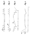
- FIGS. 2, 3 , 4 , and 5 are graphs of timing diagrams for exemplary signals generated for automatic level control of the input to the analog to digital converter of FIG. 1 .
- FIG. 1 is a block diagram of an embodiment of a digital transmission system, indicated generally and 100 , including analog to digital (A/D) converter 102 with automatic level control for an input to A/D converter 102 according to the teachings of the present invention.
- System 100 includes a main signal path, between analog input 104 and digital output 106 , and a feedback path between overflow indicator 108 and feedback control input 110 .
- the feedback path of system 100 and variable attenuator 112 of the main signal path comprise an automatic level control circuit for the input to analog to digital converter 102 . Each of these paths is discussed in turn below.
- variable attenuator 112 receives radio frequency (RF) analog signals.
- Analog input 104 is coupled to variable attenuator 112 through amplifier 114 .
- variable attenuator 112 comprises an attenuator circuit fabricated from a plurality of PIN diodes coupled in a “pi” or a “T” configuration. In other embodiments, other circuits that provided a controllable attenuation are used in place of the PIN attenuator.
- Variable attenuator 112 includes feedback control input 110 .
- Variable attenuator 112 is coupled to low pass filter 116 through amplifier 118 .
- Low pass filter 116 in one embodiment, comprises a Nyquist filter with a pass band that is designed to prevent signal aliasing.
- the main signal path of system 100 further includes analog to digital converter 102 that is coupled to the output of filter 116 through amplifier 120 .
- Analog to digital converter 102 has a peak input voltage level that is acceptable for producing a non-distorted output.
- Analog to digital converter 102 includes overflow indicator 108 . When the acceptable peak level input to analog to digital converter 102 is exceeded, overflow indicator 108 produces a number of pulses with a frequency of occurrence that is related to the degree of overload and the format of the complex input signal.
- Analog to digital converter 102 also provides an n-bit output signal to digital processing serializer 122 .
- Serializer 122 provides a serial data stream to digital transmitter 124 .
- Digital transmitter 124 provides an output to digital output 106 for system 100 .
- System 100 also includes clock 126 that provides clocking signals to analog to digital converter 102 , serializer 122 , and digital transmitter 124 .
- the feedback path of system 100 is coupled between overflow indicator 108 of analog to digital converter 102 and feedback control input 110 of variable attenuator 112 .
- the overflow indicator 108 provides an input to first peak detector 128 .
- first peak detector 128 comprises diode 130 , capacitor 132 , and resistor 134 .
- Diode 130 receives the input from overflow indicator 108 .
- Capacitor 132 is coupled between an output of diode 130 and ground.
- Resistor 134 is coupled between an output of diode 130 and a first input of amplifier 136 .
- first peak detector 128 stretches pulses from overflow indicator 108 from a range of 10 to 50 ns to approximately 300 microseconds. Based on the complexity of the input signal provided to analog to digital converter 102 , and the degree of overflow, the frequency of occurrence (period) of the stretched pulses will vary and manifest themselves in bursts of pulses ranging typically from a few microseconds wide to several milliseconds wide.
- Amplifier 136 inverts, amplifies, and level shifts the output of first peak detector 128 .
- the feedback path of system 100 further includes second peak detector 138 .
- Second peak detector 138 includes diode 140 coupled to an output of amplifier 136 .
- Second peak detector 138 also includes first and second resistors 142 and 144 , respectively.
- First resistor 142 is coupled between diode 140 and node 146 .
- Second resistor 144 is coupled between an output of amplifier 136 and node 146 .
- capacitor 148 of second peak detector 138 is coupled between node 146 and ground.
- the second peak detector 138 is designed with dual time constants that are sufficiently long relative to the burst interval such that second peak detector 138 stretches and effectively integrates both the pulses within the burst interval and the bursts themselves.
- the feedback path of system 100 further includes DC generation circuit 150 .
- Circuit 150 includes non-inverting amplifier 152 that amplifies, filters, and level shifts the output of second peak detector 138 .
- Resistor 154 in combination with capacitor 156 further filters the output of amplifier 152 .
- Circuit 150 further includes amplifier 158 that is coupled to the output of amplifier 152 .
- Amplifier 158 provides a signal to the feedback control input 110 of variable attenuator 112 . The operation of system 100 is described with respect to the timing diagrams of FIGS. 2, 3 , 4 , and 5 .
- system 100 processes analog signals for transmission as digital signals over an appropriate medium, e.g., a fiber-optic cable.
- the analog signal is received at input 104 .
- the analog signal is amplified to an appropriate level for analog to digital converter 102 by the combination of variable attenuator 112 and amplifiers 114 , 118 , and 120 .
- Variable attenuator 112 is controlled so as to assure that the peak voltage level of the analog input signal provided to analog to digital converter 102 is substantially near the acceptable peak level input for analog to digital converter 102 .
- Analog to digital converter 102 converts the analog signal to a digital output.
- the digital output of analog to digital converter 102 comprises an N-bit output signal.
- the N-bit output signal is converted to a serial signal in serializer 112 .
- digital transmitter 124 transmits the digital signal over an appropriate medium.
- Analog to digital converter 102 , digital processing serializer 122 , and digital transmitter 124 are the each controlled by clock 126 .
- analog to digital converter 102 When the input to analog to digital converter 102 exceeds a specified peak voltage level, analog to digital converter 102 produces an overflow indication at overflow indicator 108 .
- This overflow indication comprises a series of pulses. The frequency of occurrence of the pulses depends on the degree of overload of the analog to digital converter and the format of the complex input signal.
- An example of an output from overflow indicator 108 is shown by way of example in FIG. 2 .
- the pulses with, indicated at A is in the range from 10 to 50 ns.
- the period of the pulses, indicated at B is in the range from 1 to 200 microseconds.
- the feedback path of system 100 provides a control signal to variable attenuator 112 so as to selectively control the amplitude of the analog signal provided to analog to digital converter 102 such that a peak level of the analog signal is substantially near the acceptable peak input level for analog to digital converter 102 .
- First peak detector 128 stretches the pulses in overflow indicator 108 from approximately 10 to 50 ns range up to approximately 300 microseconds. Depending on the complexity of the input signal to analog digital converter 102 , and the degree of overflow, the frequency of occurrence of the stretched pulses output from first peak detector 128 will vary and manifest themselves in bursts of pulses ranging typically from a few microseconds wide to several milliseconds wide.
- first peak detector 128 in one example, is shown in FIG. 3 with the stretched pulses with a duration indicated at C.
- the pulse bursts are inverted, amplified, and level shifted by amplifier 136 to produce an output of the type shown in FIG. 4 .
- the portion of waveform 400 identified at D is a burst of stretched pulses ranging typically from a few microseconds wide to several milliseconds wide.
- the portion of waveform 400 indicated at E represents the pulse burst period that is typically from one to two milliseconds up to tens of milliseconds in duration.
- Second peak detector 138 also stretches the input from amplifier 136 . Further, due to the nature of its dual time constants, second peak detector 138 effectively integrates both the pulses within the burst interval and the burst themselves.
- the output of second peak detector 138 is shown, for example, in FIG. 5 . This output is essentially a heavily filtered DC voltage with a nominal filtered DC voltage, V AVG , that is proportional to the frequency of occurrence of the analog to digital converter overflow as indicated by overflow indicator 108 .
- the output of second peak detector 138 is further refined in DC generation circuit 150 so as to provide a voltage level to feedback control input 110 of variable attenuator 112 . Based on the changing input to analog to digital converter 102 , amplifier 158 of DC generation circuit 150 provides the appropriate current to variable attenuator 112 to keep the overflow output of the analog to digital converter at a point that will generate minimal and insignificant spurious signals.
- circuits other than peak detectors are used to condition the output of the overflow register to generate a control signal for an attenuator.
- other variable attenuators are used in place of the attenuator based on PIN diodes.
- the feedback loop is used with circuits other than digital transmitters.
- the input is adapted to receive signals other than RF input signals.
Landscapes
- Engineering & Computer Science (AREA)
- Theoretical Computer Science (AREA)
- Control Of Amplification And Gain Control (AREA)
- Analogue/Digital Conversion (AREA)
Abstract
Description
Claims (33)
Priority Applications (3)
| Application Number | Priority Date | Filing Date | Title |
|---|---|---|---|
| US09/599,701 US6657570B1 (en) | 2000-06-22 | 2000-06-22 | Automatic level control for input to analog to digital converter |
| AU2001268643A AU2001268643A1 (en) | 2000-06-22 | 2001-06-21 | Automatic level control for input to analog to digital converter |
| PCT/US2001/019822 WO2001099284A2 (en) | 2000-06-22 | 2001-06-21 | Automatic level control for input to analog to digital converter |
Applications Claiming Priority (1)
| Application Number | Priority Date | Filing Date | Title |
|---|---|---|---|
| US09/599,701 US6657570B1 (en) | 2000-06-22 | 2000-06-22 | Automatic level control for input to analog to digital converter |
Publications (1)
| Publication Number | Publication Date |
|---|---|
| US6657570B1 true US6657570B1 (en) | 2003-12-02 |
Family
ID=24400717
Family Applications (1)
| Application Number | Title | Priority Date | Filing Date |
|---|---|---|---|
| US09/599,701 Expired - Lifetime US6657570B1 (en) | 2000-06-22 | 2000-06-22 | Automatic level control for input to analog to digital converter |
Country Status (3)
| Country | Link |
|---|---|
| US (1) | US6657570B1 (en) |
| AU (1) | AU2001268643A1 (en) |
| WO (1) | WO2001099284A2 (en) |
Cited By (6)
| Publication number | Priority date | Publication date | Assignee | Title |
|---|---|---|---|---|
| US20070035429A1 (en) * | 2005-08-09 | 2007-02-15 | Richard Schreier | Delta sigma modulator system with start up transient suppression |
| DE102006025116A1 (en) * | 2006-05-30 | 2007-12-06 | Austriamicrosystems Ag | Adjustable analog-to-digital converter arrangement and method for analog-to-digital conversion |
| US20120050087A1 (en) * | 2010-08-24 | 2012-03-01 | Yasunori Aoki | Ad converter and ad converter circuit voltage control method |
| US20190280705A1 (en) * | 2018-03-08 | 2019-09-12 | Analog Devices Global Unlimited Company | Analog to digital converter stage |
| US10505561B2 (en) | 2018-03-08 | 2019-12-10 | Analog Devices Global Unlimited Company | Method of applying a dither, and analog to digital converter operating in accordance with the method |
| US10511316B2 (en) | 2018-03-08 | 2019-12-17 | Analog Devices Global Unlimited Company | Method of linearizing the transfer characteristic by dynamic element matching |
Citations (9)
| Publication number | Priority date | Publication date | Assignee | Title |
|---|---|---|---|---|
| US4851842A (en) * | 1987-07-03 | 1989-07-25 | Masayuki Iwamatsu | Analog-to-digital conversion circuit |
| US5541600A (en) * | 1993-06-28 | 1996-07-30 | Csem Centre Suisse D'electronique Et De Microtechnique Sa-Recherche Et Developpement | Signal processing circuit including a variable gain input stage |
| US5630221A (en) | 1991-12-18 | 1997-05-13 | Texas Instruments Incorporated | Dynamic range extension system |
| US5748129A (en) * | 1994-11-25 | 1998-05-05 | Nec Corporation | Analog to digital converter circuit |
| US5861831A (en) | 1996-12-23 | 1999-01-19 | Analog Devices, Inc. | Intermediate frequency (IF) sampling clock-to-clock auto-ranging analog-to-digital converter (ADC) and method |
| US5960005A (en) | 1995-12-25 | 1999-09-28 | Fujitsu Limited | Method and device for two-way communication network |
| US6150968A (en) * | 1997-12-02 | 2000-11-21 | Texas Instruments Incorporated | Trimming circuitry for pipeline A/D converter |
| US6204787B1 (en) * | 1999-03-31 | 2001-03-20 | Cirrus Logic, Inc. | Circuits and methods for gain ranging in an analog modulator and systems using the same |
| US6292120B1 (en) | 2000-03-02 | 2001-09-18 | Adc Telecommunications, Inc. | Automatic gain control for input to analog to digital converter |
-
2000
- 2000-06-22 US US09/599,701 patent/US6657570B1/en not_active Expired - Lifetime
-
2001
- 2001-06-21 AU AU2001268643A patent/AU2001268643A1/en not_active Abandoned
- 2001-06-21 WO PCT/US2001/019822 patent/WO2001099284A2/en not_active Ceased
Patent Citations (9)
| Publication number | Priority date | Publication date | Assignee | Title |
|---|---|---|---|---|
| US4851842A (en) * | 1987-07-03 | 1989-07-25 | Masayuki Iwamatsu | Analog-to-digital conversion circuit |
| US5630221A (en) | 1991-12-18 | 1997-05-13 | Texas Instruments Incorporated | Dynamic range extension system |
| US5541600A (en) * | 1993-06-28 | 1996-07-30 | Csem Centre Suisse D'electronique Et De Microtechnique Sa-Recherche Et Developpement | Signal processing circuit including a variable gain input stage |
| US5748129A (en) * | 1994-11-25 | 1998-05-05 | Nec Corporation | Analog to digital converter circuit |
| US5960005A (en) | 1995-12-25 | 1999-09-28 | Fujitsu Limited | Method and device for two-way communication network |
| US5861831A (en) | 1996-12-23 | 1999-01-19 | Analog Devices, Inc. | Intermediate frequency (IF) sampling clock-to-clock auto-ranging analog-to-digital converter (ADC) and method |
| US6150968A (en) * | 1997-12-02 | 2000-11-21 | Texas Instruments Incorporated | Trimming circuitry for pipeline A/D converter |
| US6204787B1 (en) * | 1999-03-31 | 2001-03-20 | Cirrus Logic, Inc. | Circuits and methods for gain ranging in an analog modulator and systems using the same |
| US6292120B1 (en) | 2000-03-02 | 2001-09-18 | Adc Telecommunications, Inc. | Automatic gain control for input to analog to digital converter |
Non-Patent Citations (1)
| Title |
|---|
| Patent Abstract of Japan, vol. 015, No. 330, Aug. 22, 1991. |
Cited By (14)
| Publication number | Priority date | Publication date | Assignee | Title |
|---|---|---|---|---|
| US20070035429A1 (en) * | 2005-08-09 | 2007-02-15 | Richard Schreier | Delta sigma modulator system with start up transient suppression |
| US7358879B2 (en) * | 2005-08-09 | 2008-04-15 | Analog Devices, Inc. | ΔΣ modulator system with start up transient suppression |
| DE102006025116A1 (en) * | 2006-05-30 | 2007-12-06 | Austriamicrosystems Ag | Adjustable analog-to-digital converter arrangement and method for analog-to-digital conversion |
| US20090267817A1 (en) * | 2006-05-30 | 2009-10-29 | Austriamicrosystems Ag | Adjustable Analogue-Digital Converter Arrangement and Method for Analogue-To-Digital Conversion |
| US8059020B2 (en) * | 2006-05-30 | 2011-11-15 | Austriamicrosystems Ag | Adjustable analogue-digital converter arrangement and method for analogue-to-digital conversion |
| DE102006025116B4 (en) * | 2006-05-30 | 2020-06-04 | Austriamicrosystems Ag | Adjustable analog-digital converter arrangement and method for analog-digital conversion |
| CN102377433A (en) * | 2010-08-24 | 2012-03-14 | 索尼公司 | AD converter and ad converter circuit voltage control method |
| US8493254B2 (en) * | 2010-08-24 | 2013-07-23 | Sony Corporation | AD converter and AD converter circuit voltage control method |
| CN102377433B (en) * | 2010-08-24 | 2016-11-23 | 索尼公司 | Analog-digital converter and analog-digital converter circuit voltage control method |
| US20120050087A1 (en) * | 2010-08-24 | 2012-03-01 | Yasunori Aoki | Ad converter and ad converter circuit voltage control method |
| US20190280705A1 (en) * | 2018-03-08 | 2019-09-12 | Analog Devices Global Unlimited Company | Analog to digital converter stage |
| US10505561B2 (en) | 2018-03-08 | 2019-12-10 | Analog Devices Global Unlimited Company | Method of applying a dither, and analog to digital converter operating in accordance with the method |
| US10511316B2 (en) | 2018-03-08 | 2019-12-17 | Analog Devices Global Unlimited Company | Method of linearizing the transfer characteristic by dynamic element matching |
| US10516408B2 (en) * | 2018-03-08 | 2019-12-24 | Analog Devices Global Unlimited Company | Analog to digital converter stage |
Also Published As
| Publication number | Publication date |
|---|---|
| WO2001099284A3 (en) | 2002-08-22 |
| WO2001099284A2 (en) | 2001-12-27 |
| AU2001268643A1 (en) | 2002-01-02 |
Similar Documents
| Publication | Publication Date | Title |
|---|---|---|
| US6417730B1 (en) | Automatic gain control system and related method | |
| KR920006280B1 (en) | Binary data regenerator with adaptive threshold level | |
| KR930703741A (en) | Analog / digital converter | |
| EA014210B1 (en) | Automatic gain control circuit, system including such circuit and method for automatic gain control | |
| US5450035A (en) | Automatic gain control apparatus | |
| CS268511B2 (en) | Circuit for automatic control of gain at device for signal processing | |
| US4574248A (en) | RF Power amplifier for use with VHF transceivers | |
| US4271503A (en) | Automatic control device for a receiver using a pilot | |
| US6657570B1 (en) | Automatic level control for input to analog to digital converter | |
| US5507022A (en) | Electric field level detecting apparatus | |
| US7304543B2 (en) | Burst-mode TIA (trans-impedance amplifier) | |
| US7062244B2 (en) | Speed-up mode implementation for direct conversion receiver | |
| EP0508655B1 (en) | Equalized eye pattern instrument | |
| JPH11284460A (en) | Automatic gain control amplifier | |
| JP3263017B2 (en) | Detection circuit and transmission device and reception device using the same | |
| US20060071841A1 (en) | Automatic gain control system and method | |
| EP0929150A1 (en) | A method of and a circuit for automatic gain control (AGC) | |
| CN101044683B (en) | Device for processing analog input signal and mobile communication device comprising same | |
| JPH1169333A (en) | Reception amplifier for catv | |
| JPH09270651A (en) | Automatic gain control circuit | |
| US12556151B1 (en) | Digital control of analog amplification gain in a receiver device | |
| US6411235B1 (en) | Dynamic range extension with gain correction | |
| KR20000061607A (en) | Automatic gain controller | |
| KR100660377B1 (en) | Infrared receiver using constant current and constant voltage source | |
| GB2315621A (en) | Automatic gain control for a receiver in which the need for a digital to analog converter at the output of a feedback loop is obviated by using an integrator |
Legal Events
| Date | Code | Title | Description |
|---|---|---|---|
| AS | Assignment |
Owner name: ADC TELECOMMUNICATIONS, INC., MINNESOTA Free format text: ASSIGNMENT OF ASSIGNORS INTEREST;ASSIGNOR:CHIAPPETTA, JOSEPH F.;REEL/FRAME:011214/0303 Effective date: 20000725 |
|
| AS | Assignment |
Owner name: ADC TELECOMMUNICATIONS, INC., MINNESOTA Free format text: CORRECTIVE RECORDATION FORM COVER SHEET TO REPLACE "." WITH "," WITHIN THE BODY OF THE ASSIGNMENT, PREVIOUSLY RECORDED AT REEL/FRAME 010939/0791 (ASSIGNMENT OF ASSIGNOR'S INTEREST);ASSIGNOR:CHIAPPETTA, JOSEPH F.;REEL/FRAME:012255/0803 Effective date: 20000725 |
|
| STCF | Information on status: patent grant |
Free format text: PATENTED CASE |
|
| FPAY | Fee payment |
Year of fee payment: 4 |
|
| FPAY | Fee payment |
Year of fee payment: 8 |
|
| FPAY | Fee payment |
Year of fee payment: 12 |
|
| AS | Assignment |
Owner name: TYCO ELECTRONICS SERVICES GMBH, SWITZERLAND Free format text: ASSIGNMENT OF ASSIGNORS INTEREST;ASSIGNOR:ADC TELECOMMUNICATIONS, INC.;REEL/FRAME:036060/0174 Effective date: 20110930 |
|
| AS | Assignment |
Owner name: COMMSCOPE EMEA LIMITED, IRELAND Free format text: ASSIGNMENT OF ASSIGNORS INTEREST;ASSIGNOR:TYCO ELECTRONICS SERVICES GMBH;REEL/FRAME:036956/0001 Effective date: 20150828 |
|
| AS | Assignment |
Owner name: COMMSCOPE TECHNOLOGIES LLC, NORTH CAROLINA Free format text: ASSIGNMENT OF ASSIGNORS INTEREST;ASSIGNOR:COMMSCOPE EMEA LIMITED;REEL/FRAME:037012/0001 Effective date: 20150828 |
|
| AS | Assignment |
Owner name: JPMORGAN CHASE BANK, N.A., AS COLLATERAL AGENT, ILLINOIS Free format text: PATENT SECURITY AGREEMENT (TERM);ASSIGNOR:COMMSCOPE TECHNOLOGIES LLC;REEL/FRAME:037513/0709 Effective date: 20151220 Owner name: JPMORGAN CHASE BANK, N.A., AS COLLATERAL AGENT, ILLINOIS Free format text: PATENT SECURITY AGREEMENT (ABL);ASSIGNOR:COMMSCOPE TECHNOLOGIES LLC;REEL/FRAME:037514/0196 Effective date: 20151220 Owner name: JPMORGAN CHASE BANK, N.A., AS COLLATERAL AGENT, IL Free format text: PATENT SECURITY AGREEMENT (TERM);ASSIGNOR:COMMSCOPE TECHNOLOGIES LLC;REEL/FRAME:037513/0709 Effective date: 20151220 Owner name: JPMORGAN CHASE BANK, N.A., AS COLLATERAL AGENT, IL Free format text: PATENT SECURITY AGREEMENT (ABL);ASSIGNOR:COMMSCOPE TECHNOLOGIES LLC;REEL/FRAME:037514/0196 Effective date: 20151220 |
|
| AS | Assignment |
Owner name: ALLEN TELECOM LLC, ILLINOIS Free format text: RELEASE BY SECURED PARTY;ASSIGNOR:JPMORGAN CHASE BANK, N.A.;REEL/FRAME:048840/0001 Effective date: 20190404 Owner name: COMMSCOPE, INC. OF NORTH CAROLINA, NORTH CAROLINA Free format text: RELEASE BY SECURED PARTY;ASSIGNOR:JPMORGAN CHASE BANK, N.A.;REEL/FRAME:048840/0001 Effective date: 20190404 Owner name: REDWOOD SYSTEMS, INC., NORTH CAROLINA Free format text: RELEASE BY SECURED PARTY;ASSIGNOR:JPMORGAN CHASE BANK, N.A.;REEL/FRAME:048840/0001 Effective date: 20190404 Owner name: COMMSCOPE TECHNOLOGIES LLC, NORTH CAROLINA Free format text: RELEASE BY SECURED PARTY;ASSIGNOR:JPMORGAN CHASE BANK, N.A.;REEL/FRAME:048840/0001 Effective date: 20190404 Owner name: ANDREW LLC, NORTH CAROLINA Free format text: RELEASE BY SECURED PARTY;ASSIGNOR:JPMORGAN CHASE BANK, N.A.;REEL/FRAME:048840/0001 Effective date: 20190404 Owner name: COMMSCOPE TECHNOLOGIES LLC, NORTH CAROLINA Free format text: RELEASE BY SECURED PARTY;ASSIGNOR:JPMORGAN CHASE BANK, N.A.;REEL/FRAME:049260/0001 Effective date: 20190404 Owner name: ANDREW LLC, NORTH CAROLINA Free format text: RELEASE BY SECURED PARTY;ASSIGNOR:JPMORGAN CHASE BANK, N.A.;REEL/FRAME:049260/0001 Effective date: 20190404 Owner name: REDWOOD SYSTEMS, INC., NORTH CAROLINA Free format text: RELEASE BY SECURED PARTY;ASSIGNOR:JPMORGAN CHASE BANK, N.A.;REEL/FRAME:049260/0001 Effective date: 20190404 Owner name: ALLEN TELECOM LLC, ILLINOIS Free format text: RELEASE BY SECURED PARTY;ASSIGNOR:JPMORGAN CHASE BANK, N.A.;REEL/FRAME:049260/0001 Effective date: 20190404 Owner name: COMMSCOPE, INC. OF NORTH CAROLINA, NORTH CAROLINA Free format text: RELEASE BY SECURED PARTY;ASSIGNOR:JPMORGAN CHASE BANK, N.A.;REEL/FRAME:049260/0001 Effective date: 20190404 |
|
| AS | Assignment |
Owner name: WILMINGTON TRUST, NATIONAL ASSOCIATION, AS COLLATE Free format text: PATENT SECURITY AGREEMENT;ASSIGNOR:COMMSCOPE TECHNOLOGIES LLC;REEL/FRAME:049892/0051 Effective date: 20190404 Owner name: JPMORGAN CHASE BANK, N.A., NEW YORK Free format text: ABL SECURITY AGREEMENT;ASSIGNORS:COMMSCOPE, INC. OF NORTH CAROLINA;COMMSCOPE TECHNOLOGIES LLC;ARRIS ENTERPRISES LLC;AND OTHERS;REEL/FRAME:049892/0396 Effective date: 20190404 Owner name: JPMORGAN CHASE BANK, N.A., NEW YORK Free format text: TERM LOAN SECURITY AGREEMENT;ASSIGNORS:COMMSCOPE, INC. OF NORTH CAROLINA;COMMSCOPE TECHNOLOGIES LLC;ARRIS ENTERPRISES LLC;AND OTHERS;REEL/FRAME:049905/0504 Effective date: 20190404 Owner name: WILMINGTON TRUST, NATIONAL ASSOCIATION, AS COLLATERAL AGENT, CONNECTICUT Free format text: PATENT SECURITY AGREEMENT;ASSIGNOR:COMMSCOPE TECHNOLOGIES LLC;REEL/FRAME:049892/0051 Effective date: 20190404 |
|
| AS | Assignment |
Owner name: RUCKUS WIRELESS, LLC (F/K/A RUCKUS WIRELESS, INC.), NORTH CAROLINA Free format text: RELEASE OF SECURITY INTEREST AT REEL/FRAME 049905/0504;ASSIGNOR:JPMORGAN CHASE BANK, N.A., AS COLLATERAL AGENT;REEL/FRAME:071477/0255 Effective date: 20241217 Owner name: COMMSCOPE TECHNOLOGIES LLC, NORTH CAROLINA Free format text: RELEASE OF SECURITY INTEREST AT REEL/FRAME 049905/0504;ASSIGNOR:JPMORGAN CHASE BANK, N.A., AS COLLATERAL AGENT;REEL/FRAME:071477/0255 Effective date: 20241217 Owner name: COMMSCOPE, INC. OF NORTH CAROLINA, NORTH CAROLINA Free format text: RELEASE OF SECURITY INTEREST AT REEL/FRAME 049905/0504;ASSIGNOR:JPMORGAN CHASE BANK, N.A., AS COLLATERAL AGENT;REEL/FRAME:071477/0255 Effective date: 20241217 Owner name: ARRIS SOLUTIONS, INC., NORTH CAROLINA Free format text: RELEASE OF SECURITY INTEREST AT REEL/FRAME 049905/0504;ASSIGNOR:JPMORGAN CHASE BANK, N.A., AS COLLATERAL AGENT;REEL/FRAME:071477/0255 Effective date: 20241217 Owner name: ARRIS TECHNOLOGY, INC., NORTH CAROLINA Free format text: RELEASE OF SECURITY INTEREST AT REEL/FRAME 049905/0504;ASSIGNOR:JPMORGAN CHASE BANK, N.A., AS COLLATERAL AGENT;REEL/FRAME:071477/0255 Effective date: 20241217 Owner name: ARRIS ENTERPRISES LLC (F/K/A ARRIS ENTERPRISES, INC.), NORTH CAROLINA Free format text: RELEASE OF SECURITY INTEREST AT REEL/FRAME 049905/0504;ASSIGNOR:JPMORGAN CHASE BANK, N.A., AS COLLATERAL AGENT;REEL/FRAME:071477/0255 Effective date: 20241217 |