US6586148B1 - Imaging members - Google Patents
Imaging members Download PDFInfo
- Publication number
- US6586148B1 US6586148B1 US10/059,405 US5940502A US6586148B1 US 6586148 B1 US6586148 B1 US 6586148B1 US 5940502 A US5940502 A US 5940502A US 6586148 B1 US6586148 B1 US 6586148B1
- Authority
- US
- United States
- Prior art keywords
- layer
- imaging member
- component
- accordance
- comprised
- Prior art date
- Legal status (The legal status is an assumption and is not a legal conclusion. Google has not performed a legal analysis and makes no representation as to the accuracy of the status listed.)
- Expired - Lifetime
Links
- 238000003384 imaging method Methods 0.000 title claims description 130
- 239000000203 mixture Substances 0.000 claims abstract description 44
- 239000000758 substrate Substances 0.000 claims abstract description 42
- 230000005525 hole transport Effects 0.000 claims abstract description 34
- 230000008093 supporting effect Effects 0.000 claims abstract description 25
- 239000010410 layer Substances 0.000 claims description 194
- 230000032258 transport Effects 0.000 claims description 115
- IEQIEDJGQAUEQZ-UHFFFAOYSA-N phthalocyanine Chemical compound N1C(N=C2C3=CC=CC=C3C(N=C3C4=CC=CC=C4C(=N4)N3)=N2)=C(C=CC=C2)C2=C1N=C1C2=CC=CC=C2C4=N1 IEQIEDJGQAUEQZ-UHFFFAOYSA-N 0.000 claims description 37
- 125000000217 alkyl group Chemical group 0.000 claims description 35
- 239000011230 binding agent Substances 0.000 claims description 35
- -1 polyethylene terephthalate Polymers 0.000 claims description 30
- 229910052757 nitrogen Inorganic materials 0.000 claims description 25
- 239000000049 pigment Substances 0.000 claims description 25
- KGZSDXHNEWSCQS-UHFFFAOYSA-N butyl 9-(dicyanomethylidene)fluorene-4-carboxylate Chemical group N#CC(C#N)=C1C2=CC=CC=C2C2=C1C=CC=C2C(=O)OCCCC KGZSDXHNEWSCQS-UHFFFAOYSA-N 0.000 claims description 17
- 150000004982 aromatic amines Chemical class 0.000 claims description 16
- 229910052751 metal Inorganic materials 0.000 claims description 16
- 239000002184 metal Substances 0.000 claims description 16
- 125000004432 carbon atom Chemical group C* 0.000 claims description 15
- 238000000034 method Methods 0.000 claims description 15
- 230000000903 blocking effect Effects 0.000 claims description 13
- 229920005989 resin Polymers 0.000 claims description 11
- 239000011347 resin Substances 0.000 claims description 11
- MBUWUPJZCSCIOP-UHFFFAOYSA-N 2-(2,4-dimethyl-10-oxoanthracen-9-ylidene)propanedinitrile Chemical compound C1=CC=C2C(=C(C#N)C#N)C3=CC(C)=CC(C)=C3C(=O)C2=C1 MBUWUPJZCSCIOP-UHFFFAOYSA-N 0.000 claims description 10
- UYJJFEULYOUMFZ-UHFFFAOYSA-N 2-phenylsulfanylethyl 9-(dicyanomethylidene)fluorene-4-carboxylate Chemical compound C=1C=CC=2C(=C(C#N)C#N)C3=CC=CC=C3C=2C=1C(=O)OCCSC1=CC=CC=C1 UYJJFEULYOUMFZ-UHFFFAOYSA-N 0.000 claims description 10
- 238000000576 coating method Methods 0.000 claims description 10
- 229910052736 halogen Inorganic materials 0.000 claims description 10
- 150000002367 halogens Chemical class 0.000 claims description 10
- 229920005596 polymer binder Polymers 0.000 claims description 10
- 239000002491 polymer binding agent Substances 0.000 claims description 10
- SSPXEPYZWCGXTI-UHFFFAOYSA-N 2-methylsulfanylethyl 9-(dicyanomethylidene)fluorene-4-carboxylate Chemical compound N#CC(C#N)=C1C2=CC=CC=C2C2=C1C=CC=C2C(=O)OCCSC SSPXEPYZWCGXTI-UHFFFAOYSA-N 0.000 claims description 9
- CDHJEBLYXAOBSV-UHFFFAOYSA-N 2-thiophen-3-ylethyl 9-(dicyanomethylidene)fluorene-4-carboxylate Chemical compound C=1C=CC=2C(=C(C#N)C#N)C3=CC=CC=C3C=2C=1C(=O)OCCC=1C=CSC=1 CDHJEBLYXAOBSV-UHFFFAOYSA-N 0.000 claims description 9
- 239000011248 coating agent Substances 0.000 claims description 9
- CSHWQDPOILHKBI-UHFFFAOYSA-N peryrene Natural products C1=CC(C2=CC=CC=3C2=C2C=CC=3)=C3C2=CC=CC3=C1 CSHWQDPOILHKBI-UHFFFAOYSA-N 0.000 claims description 9
- 229920000728 polyester Polymers 0.000 claims description 9
- AZQWKYJCGOJGHM-UHFFFAOYSA-N 1,4-benzoquinone Chemical compound O=C1C=CC(=O)C=C1 AZQWKYJCGOJGHM-UHFFFAOYSA-N 0.000 claims description 8
- 125000003118 aryl group Chemical group 0.000 claims description 8
- 125000002080 perylenyl group Chemical group C1(=CC=C2C=CC=C3C4=CC=CC5=CC=CC(C1=C23)=C45)* 0.000 claims description 8
- 239000004417 polycarbonate Substances 0.000 claims description 8
- 229920000515 polycarbonate Polymers 0.000 claims description 8
- 229920000139 polyethylene terephthalate Polymers 0.000 claims description 8
- 239000005020 polyethylene terephthalate Substances 0.000 claims description 8
- 239000012790 adhesive layer Substances 0.000 claims description 7
- 239000002245 particle Substances 0.000 claims description 7
- 229920002037 poly(vinyl butyral) polymer Polymers 0.000 claims description 7
- 238000001035 drying Methods 0.000 claims description 6
- 229910052739 hydrogen Inorganic materials 0.000 claims description 6
- 239000001257 hydrogen Substances 0.000 claims description 6
- 125000004435 hydrogen atom Chemical group [H]* 0.000 claims description 6
- 229910052782 aluminium Inorganic materials 0.000 claims description 5
- XAGFODPZIPBFFR-UHFFFAOYSA-N aluminium Chemical group [Al] XAGFODPZIPBFFR-UHFFFAOYSA-N 0.000 claims description 5
- 150000001412 amines Chemical class 0.000 claims description 5
- SJHHDDDGXWOYOE-UHFFFAOYSA-N oxytitamium phthalocyanine Chemical group [Ti+2]=O.C12=CC=CC=C2C(N=C2[N-]C(C3=CC=CC=C32)=N2)=NC1=NC([C]1C=CC=CC1=1)=NC=1N=C1[C]3C=CC=CC3=C2[N-]1 SJHHDDDGXWOYOE-UHFFFAOYSA-N 0.000 claims description 5
- DDTHMESPCBONDT-UHFFFAOYSA-N 4-(4-oxocyclohexa-2,5-dien-1-ylidene)cyclohexa-2,5-dien-1-one Chemical compound C1=CC(=O)C=CC1=C1C=CC(=O)C=C1 DDTHMESPCBONDT-UHFFFAOYSA-N 0.000 claims description 4
- 239000004642 Polyimide Substances 0.000 claims description 4
- 229920000265 Polyparaphenylene Polymers 0.000 claims description 4
- 239000004721 Polyphenylene oxide Substances 0.000 claims description 4
- 239000004793 Polystyrene Substances 0.000 claims description 4
- 125000003545 alkoxy group Chemical group 0.000 claims description 4
- 229920001577 copolymer Polymers 0.000 claims description 4
- 239000011159 matrix material Substances 0.000 claims description 4
- 229920001230 polyarylate Polymers 0.000 claims description 4
- 229920001601 polyetherimide Polymers 0.000 claims description 4
- 229920001721 polyimide Polymers 0.000 claims description 4
- 229920006380 polyphenylene oxide Polymers 0.000 claims description 4
- 229920002223 polystyrene Polymers 0.000 claims description 4
- 229940124530 sulfonamide Drugs 0.000 claims description 4
- 150000003456 sulfonamides Chemical class 0.000 claims description 4
- 125000000999 tert-butyl group Chemical group [H]C([H])([H])C(*)(C([H])([H])[H])C([H])([H])[H] 0.000 claims description 4
- OGGKVJMNFFSDEV-UHFFFAOYSA-N 3-methyl-n-[4-[4-(n-(3-methylphenyl)anilino)phenyl]phenyl]-n-phenylaniline Chemical compound CC1=CC=CC(N(C=2C=CC=CC=2)C=2C=CC(=CC=2)C=2C=CC(=CC=2)N(C=2C=CC=CC=2)C=2C=C(C)C=CC=2)=C1 OGGKVJMNFFSDEV-UHFFFAOYSA-N 0.000 claims description 3
- VEXZGXHMUGYJMC-UHFFFAOYSA-M Chloride anion Chemical compound [Cl-] VEXZGXHMUGYJMC-UHFFFAOYSA-M 0.000 claims description 3
- 125000002496 methyl group Chemical group [H]C([H])([H])* 0.000 claims description 3
- 229920002717 polyvinylpyridine Polymers 0.000 claims description 3
- 229920002554 vinyl polymer Polymers 0.000 claims description 3
- BUGBHKTXTAQXES-UHFFFAOYSA-N Selenium Chemical compound [Se] BUGBHKTXTAQXES-UHFFFAOYSA-N 0.000 claims description 2
- 239000011669 selenium Substances 0.000 claims description 2
- 229910052711 selenium Inorganic materials 0.000 claims description 2
- WYURNTSHIVDZCO-UHFFFAOYSA-N Tetrahydrofuran Chemical compound C1CCOC1 WYURNTSHIVDZCO-UHFFFAOYSA-N 0.000 description 16
- 239000006185 dispersion Substances 0.000 description 13
- 239000000463 material Substances 0.000 description 12
- 239000007787 solid Substances 0.000 description 10
- 108091008695 photoreceptors Proteins 0.000 description 9
- QNXWZWDKCBKRKK-UHFFFAOYSA-N 2-methyl-n-[4-[4-(n-(2-methylphenyl)anilino)phenyl]phenyl]-n-phenylaniline Chemical compound CC1=CC=CC=C1N(C=1C=CC(=CC=1)C=1C=CC(=CC=1)N(C=1C=CC=CC=1)C=1C(=CC=CC=1)C)C1=CC=CC=C1 QNXWZWDKCBKRKK-UHFFFAOYSA-N 0.000 description 8
- DIVDAELFKBKDBV-UHFFFAOYSA-N 5,8-bis(3-methylbutan-2-ylcarbamoyl)naphthalene-1,4-dicarboxylic acid Chemical compound C1=CC(C(O)=O)=C2C(C(O)=NC(C)C(C)C)=CC=C(C(O)=NC(C)C(C)C)C2=C1C(O)=O DIVDAELFKBKDBV-UHFFFAOYSA-N 0.000 description 8
- 230000008569 process Effects 0.000 description 8
- YLQBMQCUIZJEEH-UHFFFAOYSA-N tetrahydrofuran Natural products C=1C=COC=1 YLQBMQCUIZJEEH-UHFFFAOYSA-N 0.000 description 8
- YMWUJEATGCHHMB-UHFFFAOYSA-N Dichloromethane Chemical compound ClCCl YMWUJEATGCHHMB-UHFFFAOYSA-N 0.000 description 6
- MVPPADPHJFYWMZ-UHFFFAOYSA-N chlorobenzene Chemical compound ClC1=CC=CC=C1 MVPPADPHJFYWMZ-UHFFFAOYSA-N 0.000 description 6
- 239000002356 single layer Substances 0.000 description 5
- 230000015572 biosynthetic process Effects 0.000 description 4
- 230000001351 cycling effect Effects 0.000 description 4
- 239000011521 glass Substances 0.000 description 4
- 230000001976 improved effect Effects 0.000 description 4
- 238000003801 milling Methods 0.000 description 4
- 229920000642 polymer Polymers 0.000 description 4
- 239000002904 solvent Substances 0.000 description 4
- 125000000547 substituted alkyl group Chemical group 0.000 description 4
- BJEXQIZGZUTYMP-UHFFFAOYSA-N 1-methylidenefluorene-4-carboxylic acid Chemical compound C=C1C=CC(=C2C3=CC=CC=C3C=C12)C(=O)O BJEXQIZGZUTYMP-UHFFFAOYSA-N 0.000 description 3
- ZWEHNKRNPOVVGH-UHFFFAOYSA-N 2-Butanone Chemical compound CCC(C)=O ZWEHNKRNPOVVGH-UHFFFAOYSA-N 0.000 description 3
- CSCPPACGZOOCGX-UHFFFAOYSA-N Acetone Chemical compound CC(C)=O CSCPPACGZOOCGX-UHFFFAOYSA-N 0.000 description 3
- RTZKZFJDLAIYFH-UHFFFAOYSA-N Diethyl ether Chemical compound CCOCC RTZKZFJDLAIYFH-UHFFFAOYSA-N 0.000 description 3
- LFQSCWFLJHTTHZ-UHFFFAOYSA-N Ethanol Chemical compound CCO LFQSCWFLJHTTHZ-UHFFFAOYSA-N 0.000 description 3
- XEKOWRVHYACXOJ-UHFFFAOYSA-N Ethyl acetate Chemical compound CCOC(C)=O XEKOWRVHYACXOJ-UHFFFAOYSA-N 0.000 description 3
- 229920000134 Metallised film Polymers 0.000 description 3
- OKKJLVBELUTLKV-UHFFFAOYSA-N Methanol Chemical compound OC OKKJLVBELUTLKV-UHFFFAOYSA-N 0.000 description 3
- ZMXDDKWLCZADIW-UHFFFAOYSA-N N,N-Dimethylformamide Chemical compound CN(C)C=O ZMXDDKWLCZADIW-UHFFFAOYSA-N 0.000 description 3
- 206010034972 Photosensitivity reaction Diseases 0.000 description 3
- YXFVVABEGXRONW-UHFFFAOYSA-N Toluene Chemical compound CC1=CC=CC=C1 YXFVVABEGXRONW-UHFFFAOYSA-N 0.000 description 3
- 239000000654 additive Substances 0.000 description 3
- 238000007600 charging Methods 0.000 description 3
- 150000001875 compounds Chemical class 0.000 description 3
- 238000011161 development Methods 0.000 description 3
- 238000005259 measurement Methods 0.000 description 3
- 230000036211 photosensitivity Effects 0.000 description 3
- 229920002635 polyurethane Polymers 0.000 description 3
- 239000004814 polyurethane Substances 0.000 description 3
- 238000000634 powder X-ray diffraction Methods 0.000 description 3
- 239000000126 substance Substances 0.000 description 3
- XLYOFNOQVPJJNP-UHFFFAOYSA-N water Substances O XLYOFNOQVPJJNP-UHFFFAOYSA-N 0.000 description 3
- 229920002799 BoPET Polymers 0.000 description 2
- HEDRZPFGACZZDS-UHFFFAOYSA-N Chloroform Chemical compound ClC(Cl)Cl HEDRZPFGACZZDS-UHFFFAOYSA-N 0.000 description 2
- GYHNNYVSQQEPJS-UHFFFAOYSA-N Gallium Chemical compound [Ga] GYHNNYVSQQEPJS-UHFFFAOYSA-N 0.000 description 2
- LRHPLDYGYMQRHN-UHFFFAOYSA-N N-Butanol Chemical compound CCCCO LRHPLDYGYMQRHN-UHFFFAOYSA-N 0.000 description 2
- PXHVJJICTQNCMI-UHFFFAOYSA-N Nickel Chemical compound [Ni] PXHVJJICTQNCMI-UHFFFAOYSA-N 0.000 description 2
- 229910000831 Steel Inorganic materials 0.000 description 2
- GWEVSGVZZGPLCZ-UHFFFAOYSA-N Titan oxide Chemical compound O=[Ti]=O GWEVSGVZZGPLCZ-UHFFFAOYSA-N 0.000 description 2
- RTAQQCXQSZGOHL-UHFFFAOYSA-N Titanium Chemical compound [Ti] RTAQQCXQSZGOHL-UHFFFAOYSA-N 0.000 description 2
- XLOMVQKBTHCTTD-UHFFFAOYSA-N Zinc monoxide Chemical compound [Zn]=O XLOMVQKBTHCTTD-UHFFFAOYSA-N 0.000 description 2
- 238000005054 agglomeration Methods 0.000 description 2
- 230000002776 aggregation Effects 0.000 description 2
- 125000004429 atom Chemical group 0.000 description 2
- 239000011324 bead Substances 0.000 description 2
- 230000008859 change Effects 0.000 description 2
- JOTOPCOJPUYXPE-UHFFFAOYSA-N chlorobenzene Chemical compound ClC1=CC=CC=C1.ClC1=CC=CC=C1 JOTOPCOJPUYXPE-UHFFFAOYSA-N 0.000 description 2
- 125000000753 cycloalkyl group Chemical group 0.000 description 2
- JHIVVAPYMSGYDF-UHFFFAOYSA-N cyclohexanone Chemical compound O=C1CCCCC1 JHIVVAPYMSGYDF-UHFFFAOYSA-N 0.000 description 2
- 239000007888 film coating Substances 0.000 description 2
- 238000009501 film coating Methods 0.000 description 2
- 229910052733 gallium Inorganic materials 0.000 description 2
- 239000007789 gas Substances 0.000 description 2
- 150000007857 hydrazones Chemical class 0.000 description 2
- 238000004519 manufacturing process Methods 0.000 description 2
- 238000012986 modification Methods 0.000 description 2
- 230000004048 modification Effects 0.000 description 2
- 150000002979 perylenes Chemical class 0.000 description 2
- 239000011120 plywood Substances 0.000 description 2
- 229920002239 polyacrylonitrile Polymers 0.000 description 2
- 229920002451 polyvinyl alcohol Polymers 0.000 description 2
- 239000002243 precursor Substances 0.000 description 2
- 238000000518 rheometry Methods 0.000 description 2
- 238000003892 spreading Methods 0.000 description 2
- 230000007480 spreading Effects 0.000 description 2
- 239000010959 steel Substances 0.000 description 2
- VZGDMQKNWNREIO-UHFFFAOYSA-N tetrachloromethane Chemical compound ClC(Cl)(Cl)Cl VZGDMQKNWNREIO-UHFFFAOYSA-N 0.000 description 2
- 229910052719 titanium Inorganic materials 0.000 description 2
- 239000010936 titanium Substances 0.000 description 2
- 125000005259 triarylamine group Chemical group 0.000 description 2
- RYHBNJHYFVUHQT-UHFFFAOYSA-N 1,4-Dioxane Chemical compound C1COCCO1 RYHBNJHYFVUHQT-UHFFFAOYSA-N 0.000 description 1
- KIIFVSJBFGYDFV-UHFFFAOYSA-N 1h-benzimidazole;perylene Chemical class C1=CC=C2NC=NC2=C1.C1=CC(C2=CC=CC=3C2=C2C=CC=3)=C3C2=CC=CC3=C1 KIIFVSJBFGYDFV-UHFFFAOYSA-N 0.000 description 1
- XLLIQLLCWZCATF-UHFFFAOYSA-N 2-methoxyethyl acetate Chemical compound COCCOC(C)=O XLLIQLLCWZCATF-UHFFFAOYSA-N 0.000 description 1
- KXJIIWGGVZEGBD-UHFFFAOYSA-N 2-methyl-n,n-bis(2-methylphenyl)aniline Chemical compound CC1=CC=CC=C1N(C=1C(=CC=CC=1)C)C1=CC=CC=C1C KXJIIWGGVZEGBD-UHFFFAOYSA-N 0.000 description 1
- JBRZTFJDHDCESZ-UHFFFAOYSA-N AsGa Chemical compound [As]#[Ga] JBRZTFJDHDCESZ-UHFFFAOYSA-N 0.000 description 1
- 229910001369 Brass Inorganic materials 0.000 description 1
- CPELXLSAUQHCOX-UHFFFAOYSA-M Bromide Chemical compound [Br-] CPELXLSAUQHCOX-UHFFFAOYSA-M 0.000 description 1
- DKPFZGUDAPQIHT-UHFFFAOYSA-N Butyl acetate Natural products CCCCOC(C)=O DKPFZGUDAPQIHT-UHFFFAOYSA-N 0.000 description 1
- OKTJSMMVPCPJKN-UHFFFAOYSA-N Carbon Chemical compound [C] OKTJSMMVPCPJKN-UHFFFAOYSA-N 0.000 description 1
- VYZAMTAEIAYCRO-UHFFFAOYSA-N Chromium Chemical compound [Cr] VYZAMTAEIAYCRO-UHFFFAOYSA-N 0.000 description 1
- 229910001218 Gallium arsenide Inorganic materials 0.000 description 1
- FXHOOIRPVKKKFG-UHFFFAOYSA-N N,N-Dimethylacetamide Chemical compound CN(C)C(C)=O FXHOOIRPVKKKFG-UHFFFAOYSA-N 0.000 description 1
- AMQJEAYHLZJPGS-UHFFFAOYSA-N N-Pentanol Chemical compound CCCCCO AMQJEAYHLZJPGS-UHFFFAOYSA-N 0.000 description 1
- CTQNGGLPUBDAKN-UHFFFAOYSA-N O-Xylene Chemical compound CC1=CC=CC=C1C CTQNGGLPUBDAKN-UHFFFAOYSA-N 0.000 description 1
- 239000004952 Polyamide Substances 0.000 description 1
- 229910052581 Si3N4 Inorganic materials 0.000 description 1
- NINIDFKCEFEMDL-UHFFFAOYSA-N Sulfur Chemical compound [S] NINIDFKCEFEMDL-UHFFFAOYSA-N 0.000 description 1
- XSTXAVWGXDQKEL-UHFFFAOYSA-N Trichloroethylene Chemical group ClC=C(Cl)Cl XSTXAVWGXDQKEL-UHFFFAOYSA-N 0.000 description 1
- XTXRWKRVRITETP-UHFFFAOYSA-N Vinyl acetate Chemical compound CC(=O)OC=C XTXRWKRVRITETP-UHFFFAOYSA-N 0.000 description 1
- BZHJMEDXRYGGRV-UHFFFAOYSA-N Vinyl chloride Chemical compound ClC=C BZHJMEDXRYGGRV-UHFFFAOYSA-N 0.000 description 1
- 239000002253 acid Substances 0.000 description 1
- 230000003213 activating effect Effects 0.000 description 1
- 230000000996 additive effect Effects 0.000 description 1
- 239000000853 adhesive Substances 0.000 description 1
- 230000001070 adhesive effect Effects 0.000 description 1
- 150000001298 alcohols Chemical class 0.000 description 1
- 125000001931 aliphatic group Chemical group 0.000 description 1
- 150000001338 aliphatic hydrocarbons Chemical class 0.000 description 1
- 125000002947 alkylene group Chemical group 0.000 description 1
- 150000001408 amides Chemical class 0.000 description 1
- 239000012736 aqueous medium Substances 0.000 description 1
- 150000004945 aromatic hydrocarbons Chemical class 0.000 description 1
- 238000003491 array Methods 0.000 description 1
- 125000000732 arylene group Chemical group 0.000 description 1
- 239000004305 biphenyl Substances 0.000 description 1
- 239000010951 brass Substances 0.000 description 1
- 239000006229 carbon black Substances 0.000 description 1
- XOYLJNJLGBYDTH-UHFFFAOYSA-M chlorogallium Chemical compound [Ga]Cl XOYLJNJLGBYDTH-UHFFFAOYSA-M 0.000 description 1
- 229910052804 chromium Inorganic materials 0.000 description 1
- 239000011651 chromium Substances 0.000 description 1
- 239000003086 colorant Substances 0.000 description 1
- 239000004020 conductor Substances 0.000 description 1
- 230000007423 decrease Effects 0.000 description 1
- 230000001419 dependent effect Effects 0.000 description 1
- 238000000151 deposition Methods 0.000 description 1
- RAABOESOVLLHRU-UHFFFAOYSA-N diazene Chemical compound N=N RAABOESOVLLHRU-UHFFFAOYSA-N 0.000 description 1
- 229910000071 diazene Inorganic materials 0.000 description 1
- 125000000664 diazo group Chemical group [N-]=[N+]=[*] 0.000 description 1
- 239000000539 dimer Substances 0.000 description 1
- 229940113088 dimethylacetamide Drugs 0.000 description 1
- 230000009977 dual effect Effects 0.000 description 1
- 238000007786 electrostatic charging Methods 0.000 description 1
- 150000002148 esters Chemical class 0.000 description 1
- 150000002170 ethers Chemical class 0.000 description 1
- 125000001495 ethyl group Chemical group [H]C([H])([H])C([H])([H])* 0.000 description 1
- 238000001125 extrusion Methods 0.000 description 1
- RMBPEFMHABBEKP-UHFFFAOYSA-N fluorene Chemical compound C1=CC=C2C3=C[CH]C=CC3=CC2=C1 RMBPEFMHABBEKP-UHFFFAOYSA-N 0.000 description 1
- LJJQENSFXLXPIV-UHFFFAOYSA-N fluorenylidene Chemical group C1=CC=C2[C]C3=CC=CC=C3C2=C1 LJJQENSFXLXPIV-UHFFFAOYSA-N 0.000 description 1
- 229910002804 graphite Inorganic materials 0.000 description 1
- 239000010439 graphite Substances 0.000 description 1
- FUZZWVXGSFPDMH-UHFFFAOYSA-N hexanoic acid Chemical compound CCCCCC(O)=O FUZZWVXGSFPDMH-UHFFFAOYSA-N 0.000 description 1
- 230000003301 hydrolyzing effect Effects 0.000 description 1
- 125000002887 hydroxy group Chemical group [H]O* 0.000 description 1
- APHGZSBLRQFRCA-UHFFFAOYSA-M indium(1+);chloride Chemical compound [In]Cl APHGZSBLRQFRCA-UHFFFAOYSA-M 0.000 description 1
- AMGQUBHHOARCQH-UHFFFAOYSA-N indium;oxotin Chemical compound [In].[Sn]=O AMGQUBHHOARCQH-UHFFFAOYSA-N 0.000 description 1
- 230000001939 inductive effect Effects 0.000 description 1
- 229910010272 inorganic material Inorganic materials 0.000 description 1
- 239000011147 inorganic material Substances 0.000 description 1
- 239000011810 insulating material Substances 0.000 description 1
- 150000002576 ketones Chemical class 0.000 description 1
- 150000002734 metacrylic acid derivatives Chemical class 0.000 description 1
- 238000002156 mixing Methods 0.000 description 1
- PRMHOXAMWFXGCO-UHFFFAOYSA-M molport-000-691-708 Chemical compound N1=C(C2=CC=CC=C2C2=NC=3C4=CC=CC=C4C(=N4)N=3)N2[Ga](Cl)N2C4=C(C=CC=C3)C3=C2N=C2C3=CC=CC=C3C1=N2 PRMHOXAMWFXGCO-UHFFFAOYSA-M 0.000 description 1
- 229910052759 nickel Inorganic materials 0.000 description 1
- NIHNNTQXNPWCJQ-UHFFFAOYSA-N o-biphenylenemethane Natural products C1=CC=C2CC3=CC=CC=C3C2=C1 NIHNNTQXNPWCJQ-UHFFFAOYSA-N 0.000 description 1
- 230000003287 optical effect Effects 0.000 description 1
- 239000011368 organic material Substances 0.000 description 1
- 229920006287 phenoxy resin Polymers 0.000 description 1
- 239000013034 phenoxy resin Substances 0.000 description 1
- 229920003227 poly(N-vinyl carbazole) Polymers 0.000 description 1
- 229920000058 polyacrylate Polymers 0.000 description 1
- 229920002647 polyamide Polymers 0.000 description 1
- 229920005668 polycarbonate resin Polymers 0.000 description 1
- 239000004431 polycarbonate resin Substances 0.000 description 1
- 229920001296 polysiloxane Polymers 0.000 description 1
- 239000004800 polyvinyl chloride Substances 0.000 description 1
- 229920000915 polyvinyl chloride Polymers 0.000 description 1
- 238000002360 preparation method Methods 0.000 description 1
- 230000005855 radiation Effects 0.000 description 1
- 230000009467 reduction Effects 0.000 description 1
- 230000000284 resting effect Effects 0.000 description 1
- 238000012552 review Methods 0.000 description 1
- 239000000523 sample Substances 0.000 description 1
- HQVNEWCFYHHQES-UHFFFAOYSA-N silicon nitride Chemical compound N12[Si]34N5[Si]62N3[Si]51N64 HQVNEWCFYHHQES-UHFFFAOYSA-N 0.000 description 1
- 239000002002 slurry Substances 0.000 description 1
- 125000006850 spacer group Chemical group 0.000 description 1
- 239000007921 spray Substances 0.000 description 1
- 229910052717 sulfur Inorganic materials 0.000 description 1
- 239000011593 sulfur Substances 0.000 description 1
- 239000002344 surface layer Substances 0.000 description 1
- 125000006158 tetracarboxylic acid group Chemical group 0.000 description 1
- 229920005992 thermoplastic resin Polymers 0.000 description 1
- 239000004408 titanium dioxide Substances 0.000 description 1
- 238000012546 transfer Methods 0.000 description 1
- UBOXGVDOUJQMTN-UHFFFAOYSA-N trichloroethylene Natural products ClCC(Cl)Cl UBOXGVDOUJQMTN-UHFFFAOYSA-N 0.000 description 1
- 125000005287 vanadyl group Chemical group 0.000 description 1
- 238000005406 washing Methods 0.000 description 1
- 238000005303 weighing Methods 0.000 description 1
- 229910052724 xenon Inorganic materials 0.000 description 1
- FHNFHKCVQCLJFQ-UHFFFAOYSA-N xenon atom Chemical compound [Xe] FHNFHKCVQCLJFQ-UHFFFAOYSA-N 0.000 description 1
- 239000008096 xylene Substances 0.000 description 1
- 239000011787 zinc oxide Substances 0.000 description 1
Classifications
-
- G—PHYSICS
- G03—PHOTOGRAPHY; CINEMATOGRAPHY; ANALOGOUS TECHNIQUES USING WAVES OTHER THAN OPTICAL WAVES; ELECTROGRAPHY; HOLOGRAPHY
- G03G—ELECTROGRAPHY; ELECTROPHOTOGRAPHY; MAGNETOGRAPHY
- G03G5/00—Recording members for original recording by exposure, e.g. to light, to heat, to electrons; Manufacture thereof; Selection of materials therefor
- G03G5/02—Charge-receiving layers
- G03G5/04—Photoconductive layers; Charge-generation layers or charge-transporting layers; Additives therefor; Binders therefor
- G03G5/06—Photoconductive layers; Charge-generation layers or charge-transporting layers; Additives therefor; Binders therefor characterised by the photoconductive material being organic
- G03G5/0601—Acyclic or carbocyclic compounds
- G03G5/0609—Acyclic or carbocyclic compounds containing oxygen
-
- G—PHYSICS
- G03—PHOTOGRAPHY; CINEMATOGRAPHY; ANALOGOUS TECHNIQUES USING WAVES OTHER THAN OPTICAL WAVES; ELECTROGRAPHY; HOLOGRAPHY
- G03G—ELECTROGRAPHY; ELECTROPHOTOGRAPHY; MAGNETOGRAPHY
- G03G5/00—Recording members for original recording by exposure, e.g. to light, to heat, to electrons; Manufacture thereof; Selection of materials therefor
- G03G5/02—Charge-receiving layers
- G03G5/04—Photoconductive layers; Charge-generation layers or charge-transporting layers; Additives therefor; Binders therefor
- G03G5/043—Photoconductive layers characterised by having two or more layers or characterised by their composite structure
- G03G5/047—Photoconductive layers characterised by having two or more layers or characterised by their composite structure characterised by the charge-generation layers or charge transport layers
-
- G—PHYSICS
- G03—PHOTOGRAPHY; CINEMATOGRAPHY; ANALOGOUS TECHNIQUES USING WAVES OTHER THAN OPTICAL WAVES; ELECTROGRAPHY; HOLOGRAPHY
- G03G—ELECTROGRAPHY; ELECTROPHOTOGRAPHY; MAGNETOGRAPHY
- G03G5/00—Recording members for original recording by exposure, e.g. to light, to heat, to electrons; Manufacture thereof; Selection of materials therefor
- G03G5/02—Charge-receiving layers
- G03G5/04—Photoconductive layers; Charge-generation layers or charge-transporting layers; Additives therefor; Binders therefor
- G03G5/06—Photoconductive layers; Charge-generation layers or charge-transporting layers; Additives therefor; Binders therefor characterised by the photoconductive material being organic
- G03G5/0601—Acyclic or carbocyclic compounds
- G03G5/0612—Acyclic or carbocyclic compounds containing nitrogen
- G03G5/0614—Amines
- G03G5/06142—Amines arylamine
- G03G5/06144—Amines arylamine diamine
- G03G5/061443—Amines arylamine diamine benzidine
-
- G—PHYSICS
- G03—PHOTOGRAPHY; CINEMATOGRAPHY; ANALOGOUS TECHNIQUES USING WAVES OTHER THAN OPTICAL WAVES; ELECTROGRAPHY; HOLOGRAPHY
- G03G—ELECTROGRAPHY; ELECTROPHOTOGRAPHY; MAGNETOGRAPHY
- G03G5/00—Recording members for original recording by exposure, e.g. to light, to heat, to electrons; Manufacture thereof; Selection of materials therefor
- G03G5/02—Charge-receiving layers
- G03G5/04—Photoconductive layers; Charge-generation layers or charge-transporting layers; Additives therefor; Binders therefor
- G03G5/06—Photoconductive layers; Charge-generation layers or charge-transporting layers; Additives therefor; Binders therefor characterised by the photoconductive material being organic
- G03G5/0601—Acyclic or carbocyclic compounds
- G03G5/0618—Acyclic or carbocyclic compounds containing oxygen and nitrogen
-
- G—PHYSICS
- G03—PHOTOGRAPHY; CINEMATOGRAPHY; ANALOGOUS TECHNIQUES USING WAVES OTHER THAN OPTICAL WAVES; ELECTROGRAPHY; HOLOGRAPHY
- G03G—ELECTROGRAPHY; ELECTROPHOTOGRAPHY; MAGNETOGRAPHY
- G03G5/00—Recording members for original recording by exposure, e.g. to light, to heat, to electrons; Manufacture thereof; Selection of materials therefor
- G03G5/02—Charge-receiving layers
- G03G5/04—Photoconductive layers; Charge-generation layers or charge-transporting layers; Additives therefor; Binders therefor
- G03G5/06—Photoconductive layers; Charge-generation layers or charge-transporting layers; Additives therefor; Binders therefor characterised by the photoconductive material being organic
- G03G5/0622—Heterocyclic compounds
- G03G5/0624—Heterocyclic compounds containing one hetero ring
- G03G5/0635—Heterocyclic compounds containing one hetero ring being six-membered
- G03G5/0637—Heterocyclic compounds containing one hetero ring being six-membered containing one hetero atom
-
- G—PHYSICS
- G03—PHOTOGRAPHY; CINEMATOGRAPHY; ANALOGOUS TECHNIQUES USING WAVES OTHER THAN OPTICAL WAVES; ELECTROGRAPHY; HOLOGRAPHY
- G03G—ELECTROGRAPHY; ELECTROPHOTOGRAPHY; MAGNETOGRAPHY
- G03G5/00—Recording members for original recording by exposure, e.g. to light, to heat, to electrons; Manufacture thereof; Selection of materials therefor
- G03G5/02—Charge-receiving layers
- G03G5/04—Photoconductive layers; Charge-generation layers or charge-transporting layers; Additives therefor; Binders therefor
- G03G5/06—Photoconductive layers; Charge-generation layers or charge-transporting layers; Additives therefor; Binders therefor characterised by the photoconductive material being organic
- G03G5/0622—Heterocyclic compounds
- G03G5/0644—Heterocyclic compounds containing two or more hetero rings
- G03G5/0646—Heterocyclic compounds containing two or more hetero rings in the same ring system
- G03G5/0651—Heterocyclic compounds containing two or more hetero rings in the same ring system containing four relevant rings
Definitions
- an ambipolar photoconductive imaging member comprised of a supporting substrate, and thereover a layer comprised of a photogenerator hydroxygallium component, a charge transport component, and an electron transport component.
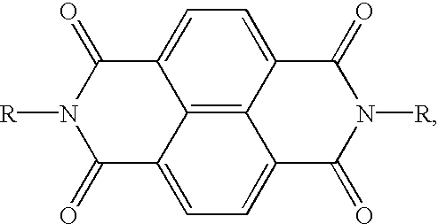
- R 1 and R 2 are independently selected from the group consisting of hydrogen, alkyl having 1 to 4 carbon atoms, alkoxy having 1 to 4 carbon atoms and halogen, and a quinone selected from the group consisting of carboxybenzylnaphthaquinone represented by the following structural formula
- This invention relates in general to imaging members and, more specifically, to negatively charged electrophotographic imaging members having an electrophotographic photoconductive insulating bilayer and processes for forming images on the member. More specifically, the present invention relates to a bilayered photoconductive imaging member containing a charge generation layer or photogenerating layer comprised of a photogenerating component, such as a photogenerating pigment, dispersed in a resin binder containing hole transporting and electron transporting molecule(s), and thereover as the second or top layer a charge transporting layer, especially a hole transport layer.
- a photogenerating component such as a photogenerating pigment
- the photogenerating layer which can be dispersed in various suitable resin binders, can be of various thicknesses, however, in embodiments a thick photogenerating layer, such as from about 3 to about 50 microns, and more specifically, from about 5 to about 20 microns is selected.
- This first layer can be considered a dual functioning layer since it can generate charge and transport charge over a wide distance, such as a distance of at least about 20 microns.
- the presence of the electron transport components in the photogenerating layer can enhance electron mobility and thus enable a thicker photogenerating layer, and which thick layers can be more easily coated than a thin layer, such as about 1 to about 2 microns thick.
- Imaging members are multilayered imaging members comprising a substrate and a plurality of other layers such as a charge generating layer and a charge transport layer. These multilayered imaging members often also contain a charge blocking layer and an adhesive layer between the substrate and the charge generating layer, and an antiplywooding layer may be selected. “Plywooding” refers, for example, in embodiments to the formation of unwanted patterns in electrostatic latent images caused by multiple reflections during laser exposure of a charged imaging member. When developed, these patterns resemble plywood. Multilayered imaging members are costly and time consuming to fabricate primarily because of the many layers that need to be formed. Further, complex equipment and valuable factory floor space are needed to manufacture multilayered imaging members. In addition to presenting plywooding problems, the multilayered imaging members often encounter charge spreading which degrades image resolution.
- High quality images are important for digital copiers, duplicators, printers, and facsimile machines, particularly laser exposure machines that demand high resolution images.
- the use of lasers to expose conventional multilayered photoreceptors can lead to the formation of undesirable plywood patterns that are visible in the final images.
- suitable high resolution electrophotographic imaging members comprised of substrate and a single electrophotographic photoconductive insulating layer in place of a plurality of layers such as a charge generating layer and a charge transport layer.
- a number of problems need to be overcome including charge acceptance for hole and/or electron transporters.
- a material mix for forming a single layer photoreceptor should possess the proper rheology and resistance to agglomeration to enable acceptable coatings.
- compatibility among pigment, hole and electron transport molecules, and film forming binder is important.
- Single electrophotographic photoconductive insulating layer refers in embodiments to, for example, a single electrophotographically active photogenerating layer capable of retaining an electrostatic charge in the dark during electrostatic charging, imagewise exposure and image development.
- a multilayered photoreceptor has at least two electrophotographically active layers, namely at least one charge generating layer and at least one separate charge transport layer.
- U.S. Pat. No. 4,265,990 a photosensitive member having at least two electrically operative layers is disclosed.
- the first layer comprises a photoconductive layer which is capable of photogenerating holes and injecting photogenerated holes into a contiguous charge transport layer.
- the charge transport second layer comprises a polycarbonate resin containing from about 25 to about 75 percent by weight of one or more of a compound having a specified general formula.
- U.S. Pat. No. 5,336,577 discloses a thick organic ambipolar layer on a photoresponsive device which is simultaneously capable of charge generation and charge transport.
- the organic photoresponsive layer contains an electron transport material, such as a fluorenylidene malonitrile derivative, and a hole transport material, such as a dihydroxy tetraphenyl benzadine containing polymer. These may be complexed to provide photoresponsivity, and/or a photoresponsive pigment or dye may also be included.
- electrophotographic imaging members comprising an electrophotographic photoconductive member layer having two layers of a thick charge generating layer overcoated with a charge transporting layer.
- It is still another feature of the present invention to provide an improved electrophotographic imaging member comprising an electrophotographic photoconductive insulating member with two layers that eliminate the need for a charge blocking layer between a supporting substrate and the electrophotographic photoconductive insulating layer.
- aspects of the present invention relate to a photoconductive member comprised of a supporting substrate, and thereover a first layer comprised of a mixture of a photogenerator component, a hole transport component, and an electron transport component; and thereover a second layer comprised of a charge transport component; an imaging member wherein the first layer is of a thickness of from about 3 to about 50 microns; an imaging member wherein the amounts for each of the components in the first layer are from about 0.05 weight percent to about 30 weight percent for the photogenerating component, from about 10 weight percent to about 75 weight percent for the charge transport component, and from about 10 weight percent to about 75 weight percent for the electron transport component, and wherein the total of these components is about 100 percent, and wherein the layer is optionally dispersed in from about 10 weight percent to about 75 weight percent of a polymer binder, and wherein the first layer is of an optional thickness of from about 5 to about 20 microns; an imaging member wherein the amounts for each of the components in the first layer mixture are from about 0.5 weight percent to about 5
- X is selected from the group consisting of an alkyl, a halogen, an aryl or mixtures thereof; an imaging member wherein alkyl contains from about 1 to about 30 carbon atoms and wherein the charge transport is an aryl amine encompassed by the above formula and which amine is optionally dispersed in a highly insulating and transparent resinous binder; an imaging member wherein alkyl contains from 1 to about 5 carbon atoms; an imaging member wherein alkyl is methyl, and wherein halogen is chloride; an imaging member wherein the charge component is comprised of N,N′-diphenyl-N,N-bis(3-methyl phenyl)-1,1′-biphenyl4,4′-diamine; an imaging member wherein the electron transport component is (4-n-butoxycarbonyl-9-fluorenylidene) malononitrile, 2-methylthioethyl 9-dicyanomethylenefluorene-4-carboxylate, 2-(3-
- each R is independently selected from the group consisting of hydrogen, alkyl optionally with 1 to 4 carbon atoms, alkoxy optionally with 1 to 4 carbon atoms and halogen, and a quinone selected from the group consisting of carboxybenzylnaphthaquinone represented by the following formula
- the second layer is comprised of hole transport components; a member wherein the hole transport is comprised of an arylamine of N,N′-diphenyl-N, N′-bis(3-methylphenyl)-[1,1′-biphenyl]-4,4′-diamine, the film forming binder is a polycarbonate, the first electrophotographic photoconductive insulating layer has a thickness of about 3 micrometers to about 50 micrometers after drying; or wherein the photogenerating photoconductive insulating layer has a thickness of about 5 micrometers to about 20 micrometers after drying, wherein the member is free of any charge blocking layer between the supporting layer and the photogenerating layer, wherein the member is free of any charge generating layer between the supporting layer and the photogenerating layer, or wherein the member is free of any antiplywood layer between the supporting layer and the photogenerating layer; a method of imaging which comprises generating an electrostatic latent
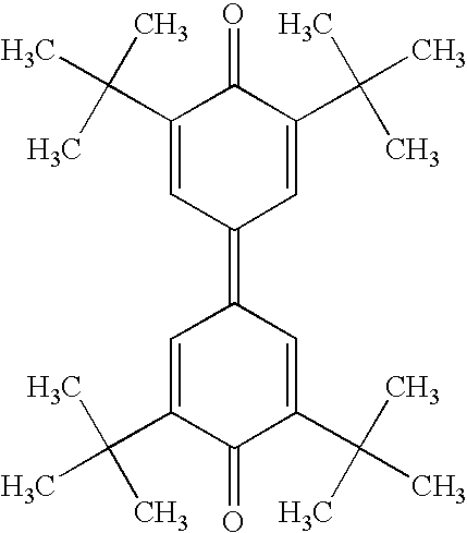
- R is selected from the group consisting of hydrogen, alkyl, branched alkyl, cycloalkyl, substituted alkyl, aryl or substituted alkyl with 1 to about 30 atoms for the aliphatic Rs and from about 6 to about 36 carbon atoms for aryl, 1,1′-Dioxo-2-(4-alkylphenyl)-6-phenyl-4-(dicyanomethylidene) thiopyran represented by the following formula
- R 1 and R 2 are independently selected from the group consisting of hydrogen, alkyl optionally with 1 to 4 carbon atoms, alkoxy optionally with 1 to 4 carbon atoms and halogen, and a quinone selected, for example, from the group consisting of carboxybenzylnaphthaquinone represented by the following formula
- a photoconductive imaging member comprised of supporting substrate, and thereover a layer comprised of a mixture of a photogenerator pigment, such as a hydroxygallium phthalocyanine component, a charge transport component, and an electron transport component; a member wherein the mixture layer is of a thickness of from about 5 to about 50 microns; a member wherein the amounts for each of the components in the mixture are from about 0.05 weight percent to about 30 weight percent for the photogenerating component, from about 10 weight percent to about 70 weight percent for the charge transport component, and from about 10 weight percent to about 70 weight percent for the electron transport component, and wherein the total of the components is about 100 percent, and wherein the layer is dispersed in from about 10 weight percent to about 75 weight percent of a polymer binder; a member wherein the amounts for each of the components is from about 0.5 weight percent to about 5 weight percent for the photogenerating component; from about 30 weight
- X is selected from the group consisting of alkyl, aryl and halogen; an imaging member wherein alkyl or aryl contains from about 1 to about 30 carbon atoms and wherein the charge transport is an aryl amine encompassed by the above formula, and which amine is dispersed in a highly insulating and transparent resin binder; an imaging member wherein alkyl contains from 1 to about 6 carbon atoms; an imaging member wherein alkyl is methyl or ethyl, and wherein halogen is chloride or bromide; an imaging member wherein the charge transport is comprised of N,N′-diphenyl-N,N-bis(3-methyl phenyl)-1,1′-biphenyl-4,4′-diamine or the triarylamines, such as illustrated in U.S.
- an imaging member wherein the electron transport component is (4-n-butoxycarbonyl-9-fluorenylidene)malononitrile, 2-methylthioethyl 9-dicyanomethylenefluorene-4-carboxylate, 2-(3-thienyl)ethyl 9-dicyanomethylenefluorene-4-carboxylate, 2-phenylthioethyl 9-dicyanomethylenefluorene-4-carboxylate, 11,11,12,12-tetracyano anthraquinodimethane, 1 ,3-dimethyl-10-(dicyanomethylene)-anthrone or N,N′-(bis alkyl or aryl)-1,4,5,8-naphthalene tetracarboxylic diimide; an imaging member wherein the photogenerating component is Type V hydroxygallium phthalocyan
- charge transport molecules such as aryl amines
- charge transport molecules for both the photogenerating mixture layer and for the top layer are aryl amines, molecules
- the electron transport is a fluorenylidene, such as (4-n-butoxycarbonyl-9-fluorenylidene)malononitrile, reference U.S. Pat. No. 4,474,865, the disclosure of which is totally incorporated herein by reference.
- the negatively charged photoresponsive imaging member of the present invention in embodiments is comprised, in the following sequence, of a supporting substrate, a single layer thereover comprised of a photogenerator layer comprised of Type V hydroxygallium phthalocyanine, charge transport molecules of N,N′-diphenyl-N,N′-bis(3-methyl phenyl)-1,1′-biphenyl-4,4′-diamine, and electron transport components of N,N′-(bis alkyl or aryl)-1,4,5,8-naphthalene tetracarboxylic diimide all preferably dispersed in a suitable resin binder, such as a polycarbonate binder, and overcoated a charge transport layer thereover comprised of aryl amine molecules dispersed in a suitable resin binder.
- a suitable resin binder such as a polycarbonate binder
- the imaging member may be imaged by depositing a uniform electrostatic charge on the imaging member exposing the imaging member to activating radiation in image configuration to form an electrostatic latent image, and developing the latent image with electrostatically attractable marking particles to form a toner image in conformance to the latent image.
- the substrate may be opaque or substantially transparent, and may comprise any suitable material having the requisite mechanical properties.
- the substrate may comprise a layer of insulating material including inorganic or organic polymeric materials, such as MYLAR® a commercially available polymer, MYLAR® coated titanium, a layer of an organic or inorganic material having a semiconductive surface layer, such as indium tin oxide, aluminum, titanium and the like, or exclusively be made up of a conductive material such as aluminum, chromium, nickel, brass and the like.
- the substrate may be flexible, seamless or rigid and may have a number of many different configurations, such as, for example, a plate, a drum, a scroll, an endless flexible belt, and the like.
- the substrate is in the form of a seamless flexible belt.
- the back of the substrate, particularly when the substrate is a flexible organic polymeric material, may optionally be coated with a conventional anticurl layer.
- this layer may be of substantial thickness, for example over 3,000 microns, or of a minimum thickness. In embodiments, the thickness of this layer is from about 75 micrometers to about 275 micrometers.
- an optional adhesive undercoat layer may be formed on the substrate.
- Typical materials selected for the undercoat layer include, for example, polyesters, polyamides, poly(vinyl butyral), poly(vinyl alcohol), polyurethane and polyacrylonitrile, and the like.
- Typical polyesters include, for example, VITEL® PE100 and PE200 available from Goodyear Chemicals, and MOR-ESTER 49,000® available from Norton International.
- the undercoat layer may have any suitable thickness, for example, from about 0.001 micrometer to about 5 micrometers, from about 0.1 micrometer to about 3 micrometers, and the like.
- the undercoat layer may contain suitable amounts of additives, for example from about 1 weight percent to about 10 weight percent, of conductive or nonconductive particles, such as zinc oxide, titanium dioxide, silicon nitride, carbon black, and the like, to enhance, for example, electrical and optical properties.
- conductive or nonconductive particles such as zinc oxide, titanium dioxide, silicon nitride, carbon black, and the like.
- the undercoat layer can be coated on to a supporting substrate from a suitable solvent.
- suitable solvents include, for example, tetrahydrofuran, dichloromethane, and the like, and mixtures thereof.
- photogenerating components are metal free phthalocyanines, metal phthalocyanines, perylenes, dimeric perylenes, and more specifically, hydroxygallium dimers, hydroxygallium phthalocyanines, chlorogallium phthalocyanines, titanyl phthalocyanines, vanadyl phthalocyanines, chloroindium phthalocyanines, and benzimidazole perylenes, such as a mixture of, for example, 60/40, 50/50, 40/60, bisbenzimidazo(2,1-a-1′,2′-b)anthra(2,1,9-def:6,5,10-d′e′f′) diisoquinoline-6,11-dione and bisbenzimidazo(2,1-a:2′,1 ′-a)anthra(2,1,9-def:6,5,10-d′e′f′)diisoquinoline-10,21-dione, and the like, inclusive of appropriate known photogenerating
- Charge transport components that may be selected for both the photogenerating mixture and the charge transport layer thereover include, for example, arylamines, and more specifically, N,N′-diphenyl-N,N-bis(3-methyl phenyl)-1,1′-biphenyl-4,4′-diamine, 9-9-bis(2-cyanoethyl)-2,7-bis(phenyl-m-tolylamino)fluorene, tritolylamine, hydrazone, N,N′-bis(3,4 dimethylphenyl)-N′′(1-biphenyl) amine, and triarylamines such as illustrated in U.S. Pat. Nos. 5,495,049 and 5,587,263, the disclosures of which are totally incorporated herein by reference; and the like.
- electron transport molecules are (4-n-butoxycarbonyl-9-fluorenylidene)malononitrile, 2-methylthioethyl 9-dicyano methylenefluorene-4-carboxylate, 2-(3-thienyl)ethyl 9-dicyanomethylene fluorene-4-carboxylate, 2-phenylthioethyl 9-dicyanomethylenefluorene-4-carboxylate, 11,11,12,12-tetracyano anthraquinodimethane, 1,3-dimethyl-10-(dicyanomethylene)-anthrone, N,N′-(bis alkyl or aryl)-1,4,5,8-naphthalene
- S is sulfur
- A is a spacer group selected from the group consisting of alkylene groups, arylene groups
- B is selected from the group consisting of alkyl groups, and aryl groups.
- Specific examples include 2-methylthioethyl 9-dicyanomethylenefluorene-4-carboxylate, 2-(3-thienyl)ethyl 9-dicyano methylenefluorene-4-carboxylate, a 2-phenylthioethyl 9-dicyano methylenefluorene-4-carboxylate, and the like.
- a suitable electron transporting molecule are N,N′-bis(alkyl or aryl)-1,4,5,8-naphthalenetetracarboxylic diimide represented by the following structural formula
- R is chosen from the group consisting of hydrogen, alkyl, branched alkyl, cycloalkyl, substituted alkyl, aryl or substituted alkyl, all having between 1 and 30 atoms.
- the photogenerating components, the electron transport components and the charge transport components can be dispersed in a suitable binder, such as polycarbonates, polyesters, polyvinylbutaryl, polysiloxanes polyarylates, polyphenylene oxides, polyphenylene sulfonamides, polyimides, polyetherimides, and polyurethanes.
- a suitable binder such as polycarbonates, polyesters, polyvinylbutaryl, polysiloxanes polyarylates, polyphenylene oxides, polyphenylene sulfonamides, polyimides, polyetherimides, and polyurethanes.
- the photogenerating pigment can be present in various amounts, such as, for example, from about 0.05 weight percent to about 30 weight percent, and more specifically, from about 0.05 weight percent to about 5 weight percent.
- Charge transport components such as hole transport molecules can be present in various effective amounts, such as in an amount of from about 10 weight percent to about 75 weight percent, and more specifically, in an amount of from about 30 weight percent to about 50 weight percent
- the electron transport molecule can be present in various amounts, such as in an amount of from about 10 weight percent to about 75 weight percent, and more specifically, in an amount of from about 5 weight percent to about 30 weight percent
- the polymer binder can be present in an amount of from about 10 weight percent to about 75 weight percent, and more specifically, in an amount of from about 30 weight percent to about 50 weight percent.
- the thickness of a single photogenerating layer can be, for example, from about 3 microns to about 50 microns, and more specifically, from about 5 microns to about 20 microns.
- the binder resin present in various suitable amounts, for example from about 5 to about 70, and more specifically, from about 10 to about 50 weight percent, may be selected from a number of known polymers such as poly(vinyl butyral), poly(vinyl carbazole), polyesters, polycarbonates, poly(vinyl chloride), polyacrylates and methacrylates, copolymers of vinyl chloride and vinyl acetate, phenoxy resins, polyurethanes, poly(vinyl alcohol), polyacrylonitrile, polystyrene, and the like.
- polymers such as poly(vinyl butyral), poly(vinyl carbazole), polyesters, polycarbonates, poly(vinyl chloride), polyacrylates and methacrylates, copolymers of vinyl chloride and vinyl acetate, phenoxy resins, polyurethanes, poly(vinyl alcohol), polyacrylonitrile, polystyrene, and the like.
- the single layer coating solvents such as ketones, alcohols, aromatic hydrocarbons, halogenated aliphatic hydrocarbons, ethers, amines, amides, esters, and the like.
- cyclohexanone cyclohexanone, acetone, methyl ethyl ketone, methanol, ethanol, butanol, amyl alcohol, toluene, xylene, chlorobenzene, carbon tetrachloride, chloroform, methylene chloride, trichloroethylene, tetrahydrofuran, dioxane, diethyl ether, dimethyl formamide, dimethyl acetamide, butyl acetate, ethyl acetate, methoxyethyl acetate, and the like.
- the photoconductive imaging members can be prepared by a number of methods, such as the coating of the components from a dispersion, and more specifically, as illustrated herein.
- the photoresponsive imaging members of the present invention can in embodiments be prepared by a number of known methods, the process parameters being dependent, for example, on the member desired.
- the photogenerating, electron transport, and hole transport components of the imaging members can be coated as solutions or dispersions onto a selective substrate by the use of a spray coater, dip coater, extrusion coater, roller coater, wire-bar coater, slot coater, doctor blade coater, gravure coater, and the like, and dried, for example, at from about 40° C. to about 200° C.
- the coating can be accomplished to provide a final coating thickness of from about 0.01 to about 30 microns after drying.
- the fabrication conditions for a given photoconductive layer can be tailored to achieve optimum performance and cost for the generation of the final members.
- Imaging members of the present invention are useful in various electrostatographic imaging and printing systems, particularly those conventionally known as xerographic processes. Specifically, the imaging members of the present invention are useful in xerographic imaging processes including printing and color processes wherein the photogenerating component, such as Type V hydroxygallium phthalocyanine can absorb light of a wavelength of from about 300 to about 950 nanometers, and preferably from about 700 to about 850 nanometers. Moreover, the imaging members of the present invention can be selected for electronic printing processes with gallium arsenide diode lasers, light emitting diode (LED) arrays which typically function at wavelengths of from 660 to about 830 nanometers.
- the photogenerating component such as Type V hydroxygallium phthalocyanine
- a toner composition comprised, for example, of thermoplastic resin, colorant, such as pigment, charge additive, and surface additives, reference U.S. Pat. Nos. 4,560,635; 4,298,697 and 4,338,390, the disclosures of which are totally incorporated herein by reference, subsequently transferring the image to a suitable substrate, and permanently affixing, for example by heat, the image thereto.
- the imaging method is similar with the exception that the exposure step can be accomplished with a laser device or image bar.
- XRPDs were determined as indicated herein that is by X-ray powder diffraction traces (XRPDs) were generated on a Philips X-Ray Powder Diffractometer Model 1710 using X-radiation of CuK-alpha wavelength (0.1542 nanometer).
- the diffractometer was equipped with a graphite monochrometer and pulse-height discrimination system. Two-theta is the Bragg angle commonly referred to in x-ray crystallographic measurements. I (counts) represents the intensity of the diffraction as a function of Bragg angle as measured with a proportional counter.
- the electron transporting materials provide, for example, the desired rheology and freedom from agglomeration during the preparation and application of the coating dispersion. Moreover, these electron transporting materials ensure substantial discharge of the photoreceptor during imagewise exposure to form the electrostatic latent image.
- a pigment dispersion was prepared by roll milling 2.15 grams of Type V hydroxygallium phthalocyanine pigment particles and 2.15 grams of poly(4,4′-diphenyl-1,1′-cyclohexane carbonate) (PCZ400, available from Mitsubishi Gas Chemical Company, Inc.) binder in 26.5 grams of tetrahydrofuran (THF) and 6.6 grams of monochlorobenzene with 280 grams of 3 millimeter diameter steel balls for about 25 to about 30 hours.
- PCZ400 poly(4,4′-diphenyl-1,1′-cyclohexane carbonate)
- Various dispersions were prepared at total solids contents of from 25 percent to 28.5 percent. The dispersions were applied with a 3 mil film coating applicator to an aluminized MYLAR® (polyethylene terephthalate) and dried at 115° C. for 60 minutes to result in a thickness for the first layer of about 10 microns.
- aluminized MYLAR® polyethylene terephthalate
- a hole transporting layer solution was prepared by weighing 1.44 grams of poly(4,4′-diphenyl-1,1′-cyclohexane carbonate) together with 0.96 gram of N,N′-diphenyl-N,N′-bis(methylphenyl)-1,1-biphenyl-4,4′-diamine and 12.5 grams of monochlorobenzene chlorobenzene. This mixture was mixed in a glass bottle until the solids were dissolved.
- the resulting solution was coated onto the above prepared Type V hydroxy gallium phthalocyanine, poly(4,4′-diphenyl-1,1′-cyclohexane carbonate), N,N′-diphenyl-N,N′-bis(methylphenyl)-1,1-biphenyl-4,4′-diamine, and N,N′-bis(1,2-dimethylpropyl)-1,4,5,8-naphthalene tetracarboxylic diimide layer using a 6 mil film applicator.
- the hole transporting layer thus obtained was dried at 115° C. for 60 minutes to provide a final total film thickness of about 25 microns.
- the thickness of the resulting dried layers was determined by capacitive measurements and a thickness gauge.
- the xerographic electrical properties of the above prepared photoconductive imaging member and other similar members can be determined by known means, including electrostatically charging the surfaces thereof with a corona discharge source until the surface potentials, as measured by a capacitively coupled probe attached to an electrometer, attained an initial value V 0 of about ⁇ 800 volts. After resting for 0.5 second in the dark, the charged members attained a surface potential of V ddp , dark development potential. Each member was then exposed to light from a filtered Xenon lamp thereby inducing a photodischarge which resulted in a reduction of surface potential to a V bg value, background potential.
- the percent of photodischarge was calculated as 100 ⁇ (V ddp ⁇ V bg )/V ddp .
- the desired wavelength and energy of the exposed light was determined by the type of filters placed in front of the lamp.
- the monochromatic light photosensitivity was determined using a narrow band-pass filter.
- the photosensitivity of the imaging member is usually provided in terms of the amount of exposure energy in ergs/cm 2 , designated as E 1 ⁇ 2 , required to achieve 50 percent photodischarge from V ddp to half of its initial value. The higher the photosensitivity, the smaller is the E 1 ⁇ 2 value.
- the E 7 ⁇ 8 value corresponds to the exposure energy required to achieve 7 ⁇ 8 photodischarge from V ddp .
- the device was finally exposed to an erase lamp of appropriate light intensity and any residual potential (V residual ) was measured.
- V residual any residual potential
- the imaging members were tested with a monochromatic light exposure at a wavelength of 780+/ ⁇ 10 nanometers and an erase light with the wavelength of 600 to 800 nanometers and intensity of 150 ergs cm 2 .
- Photoinduced discharge characteristics (PIDC) curves in a negative charging mode of the 25 micrometer thick device of Example I exhibited an E 1 ⁇ 2 of 1.8 ergs/cm 2 , an E 7 ⁇ 8 of 8.2 ergs/cm 2 and a residual potential of less than about 20 volts, such as 18 volts.
- Example II The processes of Example I were repeated except that (4-n-butoxycarbonyl-9-fluorenylidene)malononitrile, an electron transport molecule, was substituted for N,N′-bis(1,2-dimethylpropyl)-1,4,5,8-naphthalene tetracarboxylic diimide. This coating was applied to an aluminized MYLAR® substrate. The resulting device was similar in characteristics to the device of Examples I and II.
- a pigment dispersion was prepared by roll milling 2.15 grams of metal free phthalocyanine pigment particles, such as x-metal free phthalocyanines and 2.15 grams of poly(4,4′-diphenyl-1,1′-cyclohexane carbonate) (PCZ400, available from Mitsubishi Gas Chemical Company, Inc.) binder in 26.5 grams of tetrahydrofuran (THF) and 6.6 grams of monochlorobenzene with 280 grams of 3 millimeter diameter steel balls for about 2 to about 5 hours.
- metal free phthalocyanine pigment particles such as x-metal free phthalocyanines
- PCZ400 poly(4,4′-diphenyl-1,1′-cyclohexane carbonate) binder
- THF tetrahydrofuran
- monochlorobenzene monochlorobenzene
- This mixture was rolled or mixed in a glass bottle until the solids were dissolved, then 1.41 grams of the above prepared pigment dispersion were added to form a dispersion containing the metal free phthalocyanine, poly(4,4′-diphenyl-1,1′-cyclohexane carbonate), N,N′-diphenyl-N,N′-bis(methylphenyl)-1,1-biphenyl-4,4′-diamine, and N,N′-bis(1,2-dimethylpropyl)-1,4,5,8-naphthalene tetracarboxylic diimide in a solids weight ratio of (2:48:30:20) and a total solid contents of 27 percent; and rolled to mix (without milling beads).
- dispersions were prepared at total solids contents ranging from 25 percent to 28.5 percent. More than 5 dispersions prepared at these ratios were applied with a 3 mil film coating applicator to an aluminized MYLAR® (polyethylene terephthalate) and dried at 115° C. for 60 minutes to result in a thickness for the first layer of about 10 microns.
- MYLAR® polyethylene terephthalate
- a hole transporting layer solution was prepared by dissolving 1.44 grams of poly(4,4′-diphenyl-1,1′-cyclohexane carbonate) weighed along with 0.96 gram of N,N′-diphenyl-N,N′-bis(methylphenyl)-1,1-biphenyl-4,4′-diamine and 12.5 grams of monochlorobenzene chlorobenzene. This mixture was rolled in a glass bottle until the solids were dissolved.
- the solution was coated onto the previously described metal free phthalocyanine, poly(4,4′-diphenyl-1,1′-cyclohexane carbonate), N,N′-diphenyl-N,N′-bis(methylphenyl)-1,1-biphenyl4,4′-diamine, and N,N′-bis(1,2-dimethylpropyl)-1,4,5,8-naphthalene tetracarboxylic diimide layer using a 6 mil film applicator.
- the hole transporting layer thus obtained was dried at 115° C. for 60 minutes to provide a final total film thickness of about 25 microns.
- the thickness of the resulting dried layers was determined by capacitive measurements and a thickness gauge.
- the resulting bilayer member will possess, it is believed, excellent electrical stability for extended cycling.
Abstract
Description


Claims (33)


Priority Applications (1)
| Application Number | Priority Date | Filing Date | Title |
|---|---|---|---|
| US10/059,405 US6586148B1 (en) | 2002-01-31 | 2002-01-31 | Imaging members |
Applications Claiming Priority (1)
| Application Number | Priority Date | Filing Date | Title |
|---|---|---|---|
| US10/059,405 US6586148B1 (en) | 2002-01-31 | 2002-01-31 | Imaging members |
Publications (1)
| Publication Number | Publication Date |
|---|---|
| US6586148B1 true US6586148B1 (en) | 2003-07-01 |
Family
ID=22022740
Family Applications (1)
| Application Number | Title | Priority Date | Filing Date |
|---|---|---|---|
| US10/059,405 Expired - Lifetime US6586148B1 (en) | 2002-01-31 | 2002-01-31 | Imaging members |
Country Status (1)
| Country | Link |
|---|---|
| US (1) | US6586148B1 (en) |
Cited By (27)
| Publication number | Priority date | Publication date | Assignee | Title |
|---|---|---|---|---|
| US20030194626A1 (en) * | 2002-04-12 | 2003-10-16 | Jiayi Zhu | Organophotoreceptor with an electron transport layer |
| US20030211413A1 (en) * | 2002-05-10 | 2003-11-13 | Xerox Corporation. | Imaging members |
| US20040043313A1 (en) * | 2002-08-30 | 2004-03-04 | Jiayi Zhu | Organophotoreceptor with a plurality of photoconductive layers |
| US20040096761A1 (en) * | 2002-11-20 | 2004-05-20 | Xerox Corporation | Imaging members |
| US6756169B2 (en) * | 2002-07-23 | 2004-06-29 | Xerox Corporation | Imaging members |
| US20040142257A1 (en) * | 2003-01-21 | 2004-07-22 | Xerox Corporation | Solution-coatable, three-component thin film design for organic optoelectronic devices |
| US20040151996A1 (en) * | 2003-01-30 | 2004-08-05 | Xerox Corporation | Photoconductive members |
| US20050142472A1 (en) * | 2003-12-26 | 2005-06-30 | Canon Kabushiki Kaisha | Electrophotographic photosensitive member, process cartridge, and electrophotographic apparatus |
| US20050154135A1 (en) * | 2004-01-08 | 2005-07-14 | Raman Patel | Toughened polymer compositions |
| US20050287453A1 (en) * | 2004-06-29 | 2005-12-29 | Xerox Corporation | Imaging members |
| US20050287454A1 (en) * | 2004-06-29 | 2005-12-29 | Xerox Corporation | Imaging members |
| US20060204875A1 (en) * | 2005-03-11 | 2006-09-14 | Nusrallah Jubran | Charge transport materials having a 1,3,6,8-tetraoxo-1,3,6,8-tetrahydrobenzo[lmn][3,8]phenanthroline-2,7-diyl group |
| US20060210898A1 (en) * | 2005-03-16 | 2006-09-21 | Nusrallah Jubran | Charge transport materials having at least a 1,3,6,8-tetraoxo-1,3,6,8-tetrahydrobenzo[lmn][3,8]phenanthroline-2,7-diyl group |
| US7125635B2 (en) | 2003-12-23 | 2006-10-24 | Xerox Corporation | Imaging members |
| US20060281020A1 (en) * | 2005-06-13 | 2006-12-14 | Samsung Electronics Co., Ltd. | Electrophotographic photoreceptor containing naphthalenetetracarboxylic acid diimide derivatives as electron transport materials in charge generating layer and the electrophotographic imaging apparatus using the photoreceptor |
| US20060286470A1 (en) * | 2005-06-16 | 2006-12-21 | Xerox Corporation | Imaging member |
| US20060292469A1 (en) * | 2005-06-23 | 2006-12-28 | Canon Kabushiki Kaisha | Electrophotographic photosensitive member, process cartridge, and electrophotographic apparatus |
| US20060292467A1 (en) * | 2005-06-24 | 2006-12-28 | Samsung Electronics Co., Ltd. | Electrophotographic photoreceptor containing electron transporting material in a charge generating layer |
| US20070072105A1 (en) * | 2003-12-23 | 2007-03-29 | Xerox Corporation | Toners and processes thereof |
| US7291430B2 (en) * | 2002-07-02 | 2007-11-06 | Xerox Corporation | Imaging members |
| US20080305414A1 (en) * | 2007-06-11 | 2008-12-11 | Xerox Corporation. | Single layered photoconductors containing needle shaped particles |
| US20110195353A1 (en) * | 2010-02-10 | 2011-08-11 | Xerox Corporation | Single layer photoreceptor comprising high mobility transport mixtures |
| US20110207040A1 (en) * | 2010-02-19 | 2011-08-25 | Fuji Xerox Co., Ltd. | Image holding member for image forming apparatus, process cartridge, and image forming apparatus |
| US8475981B2 (en) | 2010-07-15 | 2013-07-02 | Fuji Xerox, Co., Ltd. | Image holding member for image forming apparatus, process cartridge, and image forming apparatus |
| US9125829B2 (en) | 2012-08-17 | 2015-09-08 | Hallstar Innovations Corp. | Method of photostabilizing UV absorbers, particularly dibenzyolmethane derivatives, e.g., Avobenzone, with cyano-containing fused tricyclic compounds |
| US9145383B2 (en) | 2012-08-10 | 2015-09-29 | Hallstar Innovations Corp. | Compositions, apparatus, systems, and methods for resolving electronic excited states |
| US9867800B2 (en) | 2012-08-10 | 2018-01-16 | Hallstar Innovations Corp. | Method of quenching singlet and triplet excited states of pigments, such as porphyrin compounds, particularly protoporphyrin IX, with conjugated fused tricyclic compounds have electron withdrawing groups, to reduce generation of reactive oxygen species, particularly singlet oxygen |
Citations (8)
| Publication number | Priority date | Publication date | Assignee | Title |
|---|---|---|---|---|
| US4265990A (en) | 1977-05-04 | 1981-05-05 | Xerox Corporation | Imaging system with a diamine charge transport material in a polycarbonate resin |
| US4474865A (en) | 1983-08-08 | 1984-10-02 | Xerox Corporation | Layered photoresponsive devices |
| US4587189A (en) | 1985-05-24 | 1986-05-06 | Xerox Corporation | Photoconductive imaging members with perylene pigment compositions |
| US5336577A (en) | 1991-12-30 | 1994-08-09 | Xerox Corporation | Single layer photoreceptor |
| US5473064A (en) * | 1993-12-20 | 1995-12-05 | Xerox Corporation | Hydroxygallium phthalocyanine imaging members and processes |
| US5495049A (en) | 1993-03-22 | 1996-02-27 | Fuji Xerox Co., Ltd. | Triarylamine compounds useful in electrophotographic photoreceptors |
| US5851712A (en) * | 1992-01-22 | 1998-12-22 | Mita Industrial Co., Ltd. | Electrophotosensitive material |
| JP2000019758A (en) * | 1998-07-01 | 2000-01-21 | Mita Ind Co Ltd | Negatively charged single layer type electrophotographic photoreceptor |
-
2002
- 2002-01-31 US US10/059,405 patent/US6586148B1/en not_active Expired - Lifetime
Patent Citations (9)
| Publication number | Priority date | Publication date | Assignee | Title |
|---|---|---|---|---|
| US4265990A (en) | 1977-05-04 | 1981-05-05 | Xerox Corporation | Imaging system with a diamine charge transport material in a polycarbonate resin |
| US4474865A (en) | 1983-08-08 | 1984-10-02 | Xerox Corporation | Layered photoresponsive devices |
| US4587189A (en) | 1985-05-24 | 1986-05-06 | Xerox Corporation | Photoconductive imaging members with perylene pigment compositions |
| US5336577A (en) | 1991-12-30 | 1994-08-09 | Xerox Corporation | Single layer photoreceptor |
| US5851712A (en) * | 1992-01-22 | 1998-12-22 | Mita Industrial Co., Ltd. | Electrophotosensitive material |
| US5495049A (en) | 1993-03-22 | 1996-02-27 | Fuji Xerox Co., Ltd. | Triarylamine compounds useful in electrophotographic photoreceptors |
| US5587263A (en) | 1993-03-22 | 1996-12-24 | Fuji Xerox Co., Ltd. | Electrophotographic photoreceptor using triarylamine compounds |
| US5473064A (en) * | 1993-12-20 | 1995-12-05 | Xerox Corporation | Hydroxygallium phthalocyanine imaging members and processes |
| JP2000019758A (en) * | 1998-07-01 | 2000-01-21 | Mita Ind Co Ltd | Negatively charged single layer type electrophotographic photoreceptor |
Non-Patent Citations (2)
| Title |
|---|
| Copending application U.S. Ser. No. 09/302,524, filed Apr. 30, 1999, titled "Photoconductive Members". |
| Copending application U.S. Ser. No. 09/627,283, filed Jul. 28, 2000, titled "Imaging Members Having A Single Electrophotographic Photoconductive Insulating Layer". |
Cited By (51)
| Publication number | Priority date | Publication date | Assignee | Title |
|---|---|---|---|---|
| US6890693B2 (en) * | 2002-04-12 | 2005-05-10 | Samsung Electronics Co., Ltd. | Organophotoreceptor with an electron transport layer |
| US20030194626A1 (en) * | 2002-04-12 | 2003-10-16 | Jiayi Zhu | Organophotoreceptor with an electron transport layer |
| US20030211413A1 (en) * | 2002-05-10 | 2003-11-13 | Xerox Corporation. | Imaging members |
| US7291430B2 (en) * | 2002-07-02 | 2007-11-06 | Xerox Corporation | Imaging members |
| US6756169B2 (en) * | 2002-07-23 | 2004-06-29 | Xerox Corporation | Imaging members |
| US20040043313A1 (en) * | 2002-08-30 | 2004-03-04 | Jiayi Zhu | Organophotoreceptor with a plurality of photoconductive layers |
| US7183026B2 (en) | 2002-08-30 | 2007-02-27 | Samsung Electronics Co., Ltd. | Organophotoreceptor with a plurality of photoconductive layers |
| US6946227B2 (en) * | 2002-11-20 | 2005-09-20 | Xerox Corporation | Imaging members |
| US20040096761A1 (en) * | 2002-11-20 | 2004-05-20 | Xerox Corporation | Imaging members |
| US20040142257A1 (en) * | 2003-01-21 | 2004-07-22 | Xerox Corporation | Solution-coatable, three-component thin film design for organic optoelectronic devices |
| US7056632B2 (en) * | 2003-01-21 | 2006-06-06 | Xerox Corporatioin | Solution-coatable, three-component thin film design for organic optoelectronic devices |
| US7037630B2 (en) * | 2003-01-30 | 2006-05-02 | Xerox Corporation | Photoconductive members |
| US20040151996A1 (en) * | 2003-01-30 | 2004-08-05 | Xerox Corporation | Photoconductive members |
| US7479307B2 (en) | 2003-12-23 | 2009-01-20 | Xerox Corporation | Toners and processes thereof |
| CN100442147C (en) * | 2003-12-23 | 2008-12-10 | 施乐公司 | Imaging members |
| US7125635B2 (en) | 2003-12-23 | 2006-10-24 | Xerox Corporation | Imaging members |
| US20070072105A1 (en) * | 2003-12-23 | 2007-03-29 | Xerox Corporation | Toners and processes thereof |
| US20050142472A1 (en) * | 2003-12-26 | 2005-06-30 | Canon Kabushiki Kaisha | Electrophotographic photosensitive member, process cartridge, and electrophotographic apparatus |
| US7141341B2 (en) * | 2003-12-26 | 2006-11-28 | Canon Kabushiki Kaisha | Electrophotographic photosensitive member, process cartridge, and electrophotographic apparatus |
| US20050154135A1 (en) * | 2004-01-08 | 2005-07-14 | Raman Patel | Toughened polymer compositions |
| US20050287453A1 (en) * | 2004-06-29 | 2005-12-29 | Xerox Corporation | Imaging members |
| US7297458B2 (en) * | 2004-06-29 | 2007-11-20 | Xerox Corporation | Imaging members |
| US20050287454A1 (en) * | 2004-06-29 | 2005-12-29 | Xerox Corporation | Imaging members |
| US7163771B2 (en) * | 2004-06-29 | 2007-01-16 | Xerox Corporation | Imaging members |
| US7371493B2 (en) | 2005-03-11 | 2008-05-13 | Samsung Electronics Co., Ltd. | Charge transport materials having a 1,3,6,8-tetraoxo-1,3,6,8-tetrahydrobenzo[lmn][3,8]phenanthroline-2,7-diyl group |
| US20060204875A1 (en) * | 2005-03-11 | 2006-09-14 | Nusrallah Jubran | Charge transport materials having a 1,3,6,8-tetraoxo-1,3,6,8-tetrahydrobenzo[lmn][3,8]phenanthroline-2,7-diyl group |
| US20060210898A1 (en) * | 2005-03-16 | 2006-09-21 | Nusrallah Jubran | Charge transport materials having at least a 1,3,6,8-tetraoxo-1,3,6,8-tetrahydrobenzo[lmn][3,8]phenanthroline-2,7-diyl group |
| US7449270B2 (en) | 2005-06-13 | 2008-11-11 | Samsung Electronics Co., Ltd. | Electrophotographic photoreceptor containing naphthalenetetracarboxylic acid diimide derivatives as electron transport materials in charge generating layer and the electrophotographic imaging apparatus using the photoreceptor |
| US20060281020A1 (en) * | 2005-06-13 | 2006-12-14 | Samsung Electronics Co., Ltd. | Electrophotographic photoreceptor containing naphthalenetetracarboxylic acid diimide derivatives as electron transport materials in charge generating layer and the electrophotographic imaging apparatus using the photoreceptor |
| US20060286470A1 (en) * | 2005-06-16 | 2006-12-21 | Xerox Corporation | Imaging member |
| US7390601B2 (en) * | 2005-06-16 | 2008-06-24 | Xerox Corporation | Imaging member comprising modified binder |
| US20090297218A1 (en) * | 2005-06-23 | 2009-12-03 | Canon Kabushiki Kaisha | Electrophotographic photosensitive member, process cartridge, and electrophotographic apparatus |
| US7396622B2 (en) * | 2005-06-23 | 2008-07-08 | Canon Kabushiki Kaisha | Electrophotographic photosensitive member, process cartridge, and electrophotographic apparatus |
| US7592113B2 (en) | 2005-06-23 | 2009-09-22 | Canon Kabushiki Kaisha | Electrophotographic photosensitive member, process cartridge, and electrophotographic apparatus |
| US20060292469A1 (en) * | 2005-06-23 | 2006-12-28 | Canon Kabushiki Kaisha | Electrophotographic photosensitive member, process cartridge, and electrophotographic apparatus |
| US7745083B2 (en) | 2005-06-23 | 2010-06-29 | Canon Kabushiki Kaisha | Electrophotographic photosensitive member, process cartridge, and electrophotographic apparatus |
| US20080233499A1 (en) * | 2005-06-23 | 2008-09-25 | Canon Kabushiki Kaisha | Electrophotographic photosensitive member, process cartridge, and electrophotographic apparatus |
| US20060292467A1 (en) * | 2005-06-24 | 2006-12-28 | Samsung Electronics Co., Ltd. | Electrophotographic photoreceptor containing electron transporting material in a charge generating layer |
| US20080305414A1 (en) * | 2007-06-11 | 2008-12-11 | Xerox Corporation. | Single layered photoconductors containing needle shaped particles |
| US8236469B2 (en) * | 2010-02-10 | 2012-08-07 | Xerox Corporation | Single layer photoreceptor comprising high mobility transport mixtures |
| US20110195353A1 (en) * | 2010-02-10 | 2011-08-11 | Xerox Corporation | Single layer photoreceptor comprising high mobility transport mixtures |
| US20110207040A1 (en) * | 2010-02-19 | 2011-08-25 | Fuji Xerox Co., Ltd. | Image holding member for image forming apparatus, process cartridge, and image forming apparatus |
| US8673523B2 (en) * | 2010-02-19 | 2014-03-18 | Fuji Xerox Co., Ltd. | Image holding member for image forming apparatus, process cartridge, and image forming apparatus |
| US8475981B2 (en) | 2010-07-15 | 2013-07-02 | Fuji Xerox, Co., Ltd. | Image holding member for image forming apparatus, process cartridge, and image forming apparatus |
| US9145383B2 (en) | 2012-08-10 | 2015-09-29 | Hallstar Innovations Corp. | Compositions, apparatus, systems, and methods for resolving electronic excited states |
| US9611246B2 (en) | 2012-08-10 | 2017-04-04 | Hallstar Innovations Corp. | Compositions, apparatus, systems, and methods for resolving electronic excited states |
| US9765051B2 (en) | 2012-08-10 | 2017-09-19 | Hallstar Innovations Corp. | Compositions, apparatus, systems, and methods for resolving electronic excited states |
| US9867800B2 (en) | 2012-08-10 | 2018-01-16 | Hallstar Innovations Corp. | Method of quenching singlet and triplet excited states of pigments, such as porphyrin compounds, particularly protoporphyrin IX, with conjugated fused tricyclic compounds have electron withdrawing groups, to reduce generation of reactive oxygen species, particularly singlet oxygen |
| US9926289B2 (en) | 2012-08-10 | 2018-03-27 | Hallstar Innovations Corp. | Compositions, apparatus, systems, and methods for resolving electronic excited states |
| US10632096B2 (en) | 2012-08-10 | 2020-04-28 | HallStar Beauty and Personal Care Innovations Company | Method of quenching singlet and triplet excited states of photodegradable pigments, such as porphyrin compounds, particularly protoporphyrin IX, with conjugated fused tricyclic compounds having electron withdrawing groups, to reduce generation of singlet oxygen |
| US9125829B2 (en) | 2012-08-17 | 2015-09-08 | Hallstar Innovations Corp. | Method of photostabilizing UV absorbers, particularly dibenzyolmethane derivatives, e.g., Avobenzone, with cyano-containing fused tricyclic compounds |
Similar Documents
| Publication | Publication Date | Title |
|---|---|---|
| US6586148B1 (en) | Imaging members | |
| US6946227B2 (en) | Imaging members | |
| US6756169B2 (en) | Imaging members | |
| US7070892B2 (en) | Imaging members | |
| US7074533B2 (en) | Photoconductive members | |
| US5028502A (en) | High speed electrophotographic imaging system | |
| US20030211413A1 (en) | Imaging members | |
| US7223507B2 (en) | Imaging members | |
| US20080008951A1 (en) | Imaging members and method for sensitizing a charge generation layer of an imaging member | |
| US6656650B1 (en) | Imaging members | |
| US6713220B2 (en) | Photoconductive members | |
| US6858363B2 (en) | Photoconductive imaging members | |
| CA2510492C (en) | Imaging members | |
| US5952140A (en) | Bipolar charge transport materials useful in electrophotography | |
| US7163771B2 (en) | Imaging members | |
| EP1291724A2 (en) | Blue diode laser sensitive electrophotographic photoreceptor | |
| US7291432B2 (en) | Imaging members | |
| US20040063011A1 (en) | Imaging members | |
| JP3175481B2 (en) | Electrophotographic photoreceptor | |
| US20070092817A1 (en) | Imaging member | |
| US20050260512A1 (en) | Blue diode laser sensitive photoreceptor | |
| JP2002023393A (en) | Electrophotographic photoreceptor | |
| JP2001051434A (en) | Electrophotographic photoreceptor | |
| US7390598B2 (en) | Photoreceptor with three-layer photoconductive layer | |
| JPH0720644A (en) | Organic electrophotographic photoreceptor and production thereof |
Legal Events
| Date | Code | Title | Description |
|---|---|---|---|
| AS | Assignment |
Owner name: XEROX CORPORATION, CONNECTICUT Free format text: ASSIGNMENT OF ASSIGNORS INTEREST;ASSIGNORS:GRAHAM, JOHN F.;BENDER, TIMOTHY P.;LIN, LIANG-BIH;AND OTHERS;REEL/FRAME:012573/0717;SIGNING DATES FROM 20011008 TO 20011022 |
|
| AS | Assignment |
Owner name: BANK ONE, NA, AS ADMINISTRATIVE AGENT, ILLINOIS Free format text: SECURITY AGREEMENT;ASSIGNOR:XEROX CORPORATION;REEL/FRAME:013111/0001 Effective date: 20020621 Owner name: BANK ONE, NA, AS ADMINISTRATIVE AGENT,ILLINOIS Free format text: SECURITY AGREEMENT;ASSIGNOR:XEROX CORPORATION;REEL/FRAME:013111/0001 Effective date: 20020621 |
|
| STCF | Information on status: patent grant |
Free format text: PATENTED CASE |
|
| AS | Assignment |
Owner name: JPMORGAN CHASE BANK, AS COLLATERAL AGENT, TEXAS Free format text: SECURITY AGREEMENT;ASSIGNOR:XEROX CORPORATION;REEL/FRAME:015134/0476 Effective date: 20030625 Owner name: JPMORGAN CHASE BANK, AS COLLATERAL AGENT,TEXAS Free format text: SECURITY AGREEMENT;ASSIGNOR:XEROX CORPORATION;REEL/FRAME:015134/0476 Effective date: 20030625 |
|
| AS | Assignment |
Owner name: JPMORGAN CHASE BANK, AS COLLATERAL AGENT, TEXAS Free format text: SECURITY AGREEMENT;ASSIGNOR:XEROX CORPORATION;REEL/FRAME:015722/0119 Effective date: 20030625 Owner name: JPMORGAN CHASE BANK, AS COLLATERAL AGENT,TEXAS Free format text: SECURITY AGREEMENT;ASSIGNOR:XEROX CORPORATION;REEL/FRAME:015722/0119 Effective date: 20030625 |
|
| FPAY | Fee payment |
Year of fee payment: 4 |
|
| FPAY | Fee payment |
Year of fee payment: 8 |
|
| FPAY | Fee payment |
Year of fee payment: 12 |
|
| AS | Assignment |
Owner name: XEROX CORPORATION, CONNECTICUT Free format text: RELEASE BY SECURED PARTY;ASSIGNOR:JPMORGAN CHASE BANK, N.A. AS SUCCESSOR-IN-INTEREST ADMINISTRATIVE AGENT AND COLLATERAL AGENT TO BANK ONE, N.A.;REEL/FRAME:061360/0501 Effective date: 20220822 |
|
| AS | Assignment |
Owner name: XEROX CORPORATION, CONNECTICUT Free format text: RELEASE BY SECURED PARTY;ASSIGNOR:JPMORGAN CHASE BANK, N.A. AS SUCCESSOR-IN-INTEREST ADMINISTRATIVE AGENT AND COLLATERAL AGENT TO BANK ONE, N.A.;REEL/FRAME:061388/0388 Effective date: 20220822 Owner name: XEROX CORPORATION, CONNECTICUT Free format text: RELEASE BY SECURED PARTY;ASSIGNOR:JPMORGAN CHASE BANK, N.A. AS SUCCESSOR-IN-INTEREST ADMINISTRATIVE AGENT AND COLLATERAL AGENT TO JPMORGAN CHASE BANK;REEL/FRAME:066728/0193 Effective date: 20220822 |